When I was about ten my father brought a few NIXIE tubes with him home
from work (ZM1020 and B5092, I still have them see photograph).
We mounted one of them on a wooden sigar box and connected the
anode via a large series resistance to the live wire of the 220V mains!
Just by touching one of the cathodes it was possible to make the numbers
glow. 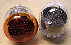 I think that this was the beginning of my life long fascination for
these misteriously glowing tubes. They are in one word beautifull!
One of the things that makes them so fascinating is that they are so visably
a monument of a time when a revolution in electronics was taking place.
On one hand they were obviously a product from the radio tube area, and on
the other hand they were used to display the results from the children
of the revolution, digital ICs. To me, an equally fascinating component
is the 74141 NIXIE driver. What a curious component it is, designed to
interface the 5V TTL world with the high voltage NIXIE tubes.
I think that this was the beginning of my life long fascination for
these misteriously glowing tubes. They are in one word beautifull!
One of the things that makes them so fascinating is that they are so visably
a monument of a time when a revolution in electronics was taking place.
On one hand they were obviously a product from the radio tube area, and on
the other hand they were used to display the results from the children
of the revolution, digital ICs. To me, an equally fascinating component
is the 74141 NIXIE driver. What a curious component it is, designed to
interface the 5V TTL world with the high voltage NIXIE tubes.
My father used to buy, from time to time, electronics magazines which I as
a child of course would read.
 Of course I could not understand everything that was in them.
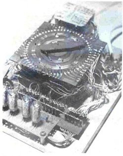
One of these magazines contained a description of a poor man's NIXIE clock
(right picture)
which used a mechanical clock to switch the cathodes of the tubes [1].
At that time I had no clue about the working of digital ICs (I was twelve),
but this was something I could understand. Over the years I built up a small
collection of NIXIE tubes, always having in mind that one day I would build
my own NIXIE clock.
Of course I could not understand everything that was in them.
One of these magazines contained a description of a poor man's NIXIE clock
(right picture)
which used a mechanical clock to switch the cathodes of the tubes [1].
At that time I had no clue about the working of digital ICs (I was twelve),
but this was something I could understand. Over the years I built up a small
collection of NIXIE tubes, always having in mind that one day I would build
my own NIXIE clock.
A few years ago a shared my room at work with Jacco van der Hoeven. Although Jacco is a mechanic by profession, he also likes to experiment with electronics in his spare time and therefor could understand my fascination for these glowing tubes. Somewhere in 2003 the NIXIE clock fever rose to an alarming level when I run into a bunch (50!) of old 74141 NIXIE driver ICs that were about to be thrown away together with a whole chest full of obsolete TTL ICs. There were at the time two obstacles which prevented me from actually building a clock. The first obstacle was the housing. Making the electronic part of the clock is no problem, but making a descent box around it is for me impossible. I always end up fitting my projects into luncheon boxes or transparant cereals containers. Although I have a very understanding wife, this is unfortunately not her idea of a nice drawing room assesoiry! The second obstacle was the lack of time. At that moment I was writing my thesis, which practically consumed all my spare time.
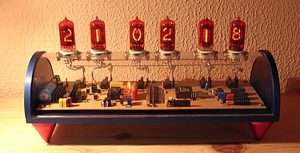
When I finally received my PhD (2 june 2004), Jacco and Eugene Timmering
organized a beautifull group present. Jacco persuaded Jim Oostveen
to donate six ZM1030 NIXIE tubes he had lying around. Then they asked
Henk van Aken from the mechanical workshop to make a beautifull housing
to hold the tubes and the electronics that would drive them. Henk is a man
who can make anything, and the result was fantastic (top figure).
Jacco and Eugene rightfully assumed that now my thesis was finished
I would have plenty of spare time left to design and built the
circuits for the clock. On these page you find a report on this delightfull
task which made a boyhood dream come true.
The ZM1030 and ZM1032 are to my knowledge the only dual anode NIXIE tubes
ever made. The tubes are identical except that the ZM1030 has a red filter
coating. The tubes were fabricated to fit into a standard NOVAL socket. A NOVAL
socket has nine pins. A normal NIXIE tube however requires at least
elleven pins (ten for the digit cathodes and one for the anode). To make
the NIXIE tube fit into a a nine pin socket, Philips used multiplexing.
Instead of just a single anode, the ZM1030 contains two anodes (Fig. 1). One
anode drives the odd digits, while the other anode drives the even digits.
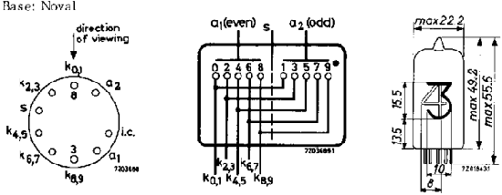
Figure 1 Connections of the ZM1030 and ZM1032 NIXIE tubes.
Now, although this sounds simple, correct driving of these tubes is not a
trivial matter. Figure 2 summarizes the driving voltages recommended
in the ZM1030 datasheet. Both the cathodes as well as the anodes are
switched between certain voltage levels. Additionally the screen between
the two anode sections in the tube has to be set to a specific voltage
level (Vbs). All this is nescassery to prevent parasitic
glow of adjacent numerals.
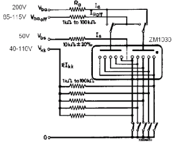
Figure 2 Driving voltages as recommended in the ZM1030 datasheet.
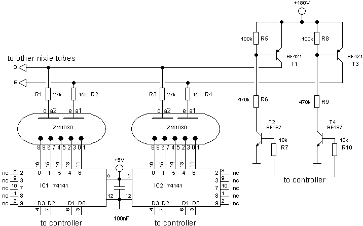
Figure 3 Basic driver circuit for the ZM1030
Multiplexing of NIXIE tubes is normally not considered to be a sensible thing.
Although with multiplexed tubes the avarage current remains the same, the
peak current increases resulting in a reduced life expectancy. No multiplexing
at all would mean that the anode driver circuit consisting of T1-T4 would
have to be repeated for every tube. Additionally two control outputs from the
microcontroller per tube would be needed.
 I choose for a compromise between
full multiplexing and no multiplexing at all. In this scheme one anode driver
circuit drives all the anodes which have been connected in parallel.
The odd and even anodes are switched on alternatedly fast enough to make the digits
appear to burn constantly. During the on time the current has to
doubled compared to the current of a continuously burning tube with the same
brightness. The anode currents are set by R1-R4 and amount to 1.4 mA for anode
a2 (odd digits) and 2.6 mA for anode a1 (even digits). This corresponds to an
avarage current of 0.7 mA and 1.3 mA respectively. The reason that the even
digits are driven by a somewhat higher current is that they are physically
located at the backside of the tube and thus obscured by the odd digits.
The higher current gives them the same brighness. Both the peak as well as
the average cathode currents are still well below the 5 mA maximum current
specified in the datasheet.
Using the tubes at an as low as possible current will
greatly extend the life expectancy of the tube. By the way, the life
expectancy at 4 mA digit current is specified in the datasheet
to be 50.000 hrs (6 years). The anodes of the tube are directly connected
via the anode resistors to two anode driver bars located on either side of
the tube sockets (figure to the left). This keeps the amount of wireing
required to the minimum.
I choose for a compromise between
full multiplexing and no multiplexing at all. In this scheme one anode driver
circuit drives all the anodes which have been connected in parallel.
The odd and even anodes are switched on alternatedly fast enough to make the digits
appear to burn constantly. During the on time the current has to
doubled compared to the current of a continuously burning tube with the same
brightness. The anode currents are set by R1-R4 and amount to 1.4 mA for anode
a2 (odd digits) and 2.6 mA for anode a1 (even digits). This corresponds to an
avarage current of 0.7 mA and 1.3 mA respectively. The reason that the even
digits are driven by a somewhat higher current is that they are physically
located at the backside of the tube and thus obscured by the odd digits.
The higher current gives them the same brighness. Both the peak as well as
the average cathode currents are still well below the 5 mA maximum current
specified in the datasheet.
Using the tubes at an as low as possible current will
greatly extend the life expectancy of the tube. By the way, the life
expectancy at 4 mA digit current is specified in the datasheet
to be 50.000 hrs (6 years). The anodes of the tube are directly connected
via the anode resistors to two anode driver bars located on either side of
the tube sockets (figure to the left). This keeps the amount of wireing
required to the minimum.
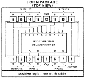 The driving
scheme presented in Fig. 3 uses only 5 of the 10 outputs
of the 74141 (see connections of 74141 on the right).
Any of the 10 outputs of the 74141 could have been used to drive
the five cathodes. The reason that outputs 0,1,5,4 and 6 have been used is that
these outputs are located on the same side of the IC, opposite to the low voltage
inputs which are connected to the microcontroller.
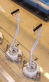
I use a simple small five pin SIL (Single-In-Line) connecter to connect the tubes
to the decoder (see picture above).
The female part of the connecter is placed next to the decoder
and connected to the decoder with straight short wires (Fig. 12).
Figure 4 shows the breadboard
testing of the driver circuit including the flyback converter. The box on
the right which holds the NIXIE tube is my "tube-test-box". It contains
a Noval, a Rimlock and a 7 pin miniature socket. The pins of the socket
are available on the top of the box via a standard sets wire plug.
For tubes with a fillament the box contains a small 6.3V transformer.
The driving
scheme presented in Fig. 3 uses only 5 of the 10 outputs
of the 74141 (see connections of 74141 on the right).
Any of the 10 outputs of the 74141 could have been used to drive
the five cathodes. The reason that outputs 0,1,5,4 and 6 have been used is that
these outputs are located on the same side of the IC, opposite to the low voltage
inputs which are connected to the microcontroller.
I use a simple small five pin SIL (Single-In-Line) connecter to connect the tubes
to the decoder (see picture above).
The female part of the connecter is placed next to the decoder
and connected to the decoder with straight short wires (Fig. 12).
Figure 4 shows the breadboard
testing of the driver circuit including the flyback converter. The box on
the right which holds the NIXIE tube is my "tube-test-box". It contains
a Noval, a Rimlock and a 7 pin miniature socket. The pins of the socket
are available on the top of the box via a standard sets wire plug.
For tubes with a fillament the box contains a small 6.3V transformer.
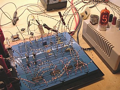
Figure 4 Breadboard testing of the driver and flyback converter circuits.
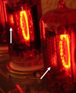
Figure 5 Parasitic glowing around digit 1 when digit 0 is selected.
For the timebase of an electronic clock their are basically two options.
Traditionally the mains frequency is used in mains powered electric/electronic
clocks. However, most people tend to prefer a crystal oscillator over the
mains frequency as a timebase for their clocks. Without question it is true that
the short term stability of a crystal oscillator is much better compared to the
mains frequency. The short term stability of the mains frequency, or rather the
phase, depends on the demand and supply of the power on the electricity grid.
When the demand increases, it "slows down" the generator. In other words it
decreases the frequency. However, the electricity companies closely monitor
the mains frequency. They count the number of cycles and compare them against
absolute time standards. When a deviation is detected, it is compansated for
at a suitabel moment. So the long term stability of the mains frequency is
excellent! On the website of ETRANS, the coordination company for the Swiss
extra high voltage grid, you can check for yourself how the mains frequency and phase
compare against the absolute time [3 but also 4,5]. Crystal oscillators
furthermore require accurate callibration, and are sensitive to temperature
fluctuations. In short, the mains frequency is an excellent choice for the timebase
of your homemade clock!
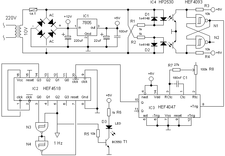
Figure 6 Mains driven 1 Hz timebase circuit.
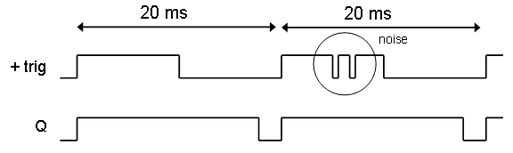
Figure 7 Timing of the input and output signals of the HEF4047. The HEF4047 one-shot is used in the non re-triggerable mode to suppress unwanted triggers.
Now most likely all this will sound to most people as an enormous overkill.
I tend to agree, but fact remains that the clocks that I have built which have
this timebase circuit are perfectly accurate.
The complete circuit will hold little surprises after all that has been discussed
in the previous sections.
The clock uses the
flyback converter discussed on one of my other pages to generate
the 180V anode voltage.
Figure 8 shows the the CPU, ISP interface and the Nixie
cathode and anode drivers. Figure 9 depicts the power supply, flyback converter,
and the 1 Hz timebase circuit. Both figures are just meant to give an overview
of the circuit. A detailed circuit diagram can be obtained in pdf format by clicking
on the pictures.

Figure 8 CPU and Nixie drivers.
(Click on the diagram to download a detailed circuit diagram in pdf format)
A very usefull feature of the P89C51RB2 is that it is possible to program the
processor without the need to remove the device from the circuit board.
Hidden somewhere in the processor is a program that allows you to erase, program
and check the on-board flash memory via the RxD and TxD serial I/O pins.
This program is activated by applying specific voltage conditions to
the EA and PSEN pins during a reset. During the development of the program,
the CPU was connected to my PC via a homebrew interface board using the
small ISP (In System Programming) connector drawn in the circuit diagram.
I will give a full description of both the interface board and the ISP programming
software on a seperate web page.
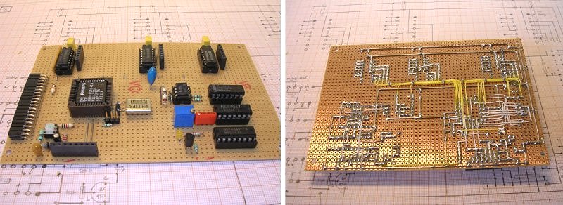
Figure 9 Front and backside of the CPU and 1Hz timebase generator board. The ISP interface connector is situated in front of the CPU.
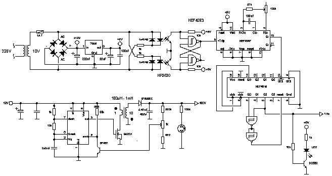
Figure 10 Power supply, flyback converter and 1Hz timebase generator.
(Click on the diagram to download a detailed circuit diagram in pdf format)
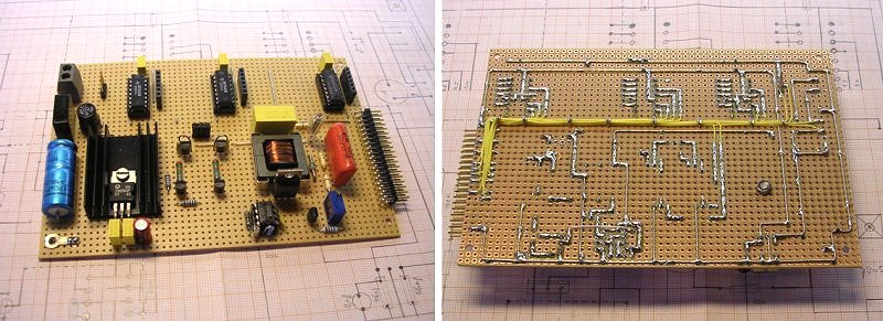
Figure 11 Front and backside of the power supply and flyback board.
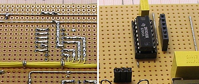
Figure 12 Close up of the connections to the 74141 Nixie driver.
Personally I hate control buttons and switches, principally because you need to drill or saw holes in the clock which is something I do not like. Additionally they require wiring and consume I/O ports. For this reason my clocks only use a single push-button control in combination with a simple menu displayed on the clock itself.
After power-up or reset, the clock enters the mode select state. In this state all digits except for the most right display (seconds) are dimmed. The most right display counts at seconds intervals from 0 to 6 and then loops around to 0 again. By pressing the control button at the appropriate moment one of the 7 modes (0-6) is selected.
The 89C51RB2 is fully 80C51 compatible. Additionally it has many features which have not been used in this clock. The control program was written in assembler, and assembled with my "standard" assembler ASM51. The ASM51 assembler for 8051 cores was written by A.C. Verschuren and denoted to the public domain in September 1987. ASM51 runs directly under DOS and is run by the command: ASM51 filename.ASM. It is very simple to work with, transparant and on modern systems extremely fast. And yet the total program is just 50kB in size, just the size of one of the highly compressed pictures on this page! I have included both the assembler and the manual in the download zip file at the end of this page.
The program itself is rather straightforward and the assembler code is reasonably well documented. I will suffice here with a brief description. To fascilitate multiplexing of the tubes, the program uses two sets of registers, the "even set": p0_e, p1_e, p2_e and the "odd set": p0_o, p1_o, p2_e. The program every 10 ms alternately writes each set of registers to the output ports. The odd set when the odd anodes are activated for the odd numbers and the even set when the even anodes are activated.
At startup the program will configure timer 1 in such a way that it will generate an interrupt every 250us. After fourty interrupts (10 ms) the interrupt service routine (T1_int) will update the output ports as described. Additionally the service routine will read and debounce the control button. After initialisation the program enters the main program loop (main). The main loop will first check for a new second. If there is a new second it will call "inctime" to update the time kept in registers "hrs", "min" and "sec". Next routine "chk_blnk" is called to implement the "night savings function". finally the routine "convert" translates the time into the proper codes for the odd and even sets of output registers. Additionally, the main loop checks if a key is pressed and implements the mode selection state.
The routine "convert" in turn uses routines "bcd2nix" and "hrs2nix".
Routine "bcd2nix" is used for the translation of the seconds and minutes
digits while "hrs2nix" is used for the translation of the hours.
Note that the hardware connections to the hours drivers are slightly different
from the minutes and seconds.
The compressed file which can be downloaded here , contains the following files:

My Son Geert's view of a father with a nixie addiction.