 |
 |
 |
|
|
|
|
Contents:
|
|
A bit of history
The first ideas for a pulsed tube curve tracer were conceived as far back as Christmas 2010. The first uTracer version used a high-side current sense circuit that did not really work satisfactorily. After a golden tip from somebody following my weblog, I changed the current sense circuit to its present concept, and the uTracer3 was born. Stimulated by my sons ōto go commercial,ö I designed a PCB for the uTracer3 in 2012 and later that year the first uTracer kits were on their way to the first customers.
How does such an undertaking work in practice? Of course the first experimental versions of the uTracer were constructed with components I had lying around. With the circuit working very satisfactorily, it was not more than logical to copy the circuit one-to-one for the commercial version of the uTracer3. At the time I estimated that perhaps, with a bit of luck, we would sell a few dozens of kits. I absolute could not have imagined that 12 years later there would be over 2600 uTracers in service in 63 countries!
Over the years, I discovered and experienced things that also real, large compagnies have to deal with. One of these things is that once you have a product running, it is not so easy to make changes to it. Over the years there have been two major changes to the design of the original uTracer. The first major change was the introduction of the uTracer3+ which raised the maximum voltage to 400 V, and the second change was a redesign of the PCB. Every change requires adaptation of the manual, changes in the components to be ordered, the production of a test series to make sure the kit is flawless, etc. Additionally, there is the issue of customer support. The uTracer is a rather complicated kit, and unavoidably mistakes happen during its construction. I always try to help everybody as good as I can via email, and if that doesnÆt work out I am happy to have a look at the circuit myself, so you really want to limit the number of circuit versions to deal with to the minimum. In short, the choices you make in the beginning in terms of component selection and circuit topology may very well haunt you for years!
One of the things every electronic appliance company that sells products that run over many years must deal with, is that at a certain moment components become obsolete. It happens to big companies, like Philips where I work(ed), and tiny companies like Dos4ever. At a certain moment for example, it was announced that the original processor, the PIC16F874 would be taken out of production. The PIC16F884 was suggested as an almost pin compatible alternative. Nevertheless, it took me days of headache and many software changes to get it working. Also the original MJE350 and KSP99 high-voltage pnp transistors in the meantime have been phased out and had to be replaced with suitable alternatives.
The latest addition to the list of ōsoon to be obsoleteö components is the DIL version of the OPA227! Already since COVID times, the availability of the OPA227 has given me a headache, while also since that time its price has skyrocketed! Apparently the SMD/SMT version of the OPA227 will remain in production somewhat longer, so to mitigate the upcoming problem, my first idea was to redesign the PCB to make it suitable for the SMD variant. However, thinking things over I started doubting if this would be the right way to go?
I have always been a strong fan of ōold fashionedö through-hole components. Primarily, because most uTracer customers are tube/valve enthusiasts who, very often, do not have much affinity with tiny, fragile, difficult to handle and solder SMD components. Secondly, I always had the idea that servicing a circuit with through-hole components was easier than servicing a PCB with SMD components. I learned that although this certainly holds for ICÆs in sockets, where the possibility of rapidly exchanging a part helps to quickly debug the circuit, I discovered that the situation may be completely the opposite for other components. Ever since I started using a hot air soldering station, I realized that especially replacing transistors is much easier if you have an SMD component instead of its through-hole counterpart! On top of that, the harsh reality is that many modern and powerful components are simply not available in through-hole packages anymore!
So, all this made me think and decided me not to go for a straightforward simple modification of the uTracer3 PCB, but instead to take a critical look at the whole circuit and come up with a more modern and future proof overhault: the uTracerNXT!
WhatÆs in a name?
Being a man of exact science (and a bit autistic as well), my first idea was to name the redesign of the uTracer the - you may have guessed it - uTracer3.2. However, after hearing me talk about the uTracer3.2 for weeks, the CEO of our tiny family enterprise (my wife) expressed her discontent with the name. First of all, she thought it looked ōugly,ö but she also thought that it was rather nondescriptive, not doing justice to the fact that the new design will also include a substantial number of innovations and improvements. ōItÆs a bit how kings or popes are numberedö was here objection. Since we already have a uTracer 4, 5, 6, 7 (that not all made it into a kit by the way) I started thinking of an alternative. For a moment I was tempted to call it the ōFU2Tracer,ö but I am glad I was sensible and didnÆt go that route. Playing with words and letters I came up with NXTracer (Next Tracer) to emphasize that the new tracer is not just an upgrade of the old uTracer3+, but really a completely new design. However, then several readers pointed out to me that it would not be a good idea to discard the, in the mean time, well-known brand name uTracer (micro-Tracer), so in the end we settled for uTracerNXT, to be pronounced ōMicro-Tracer Nextö I tested the new name on my wife and sons, and they all liked it. So, there we have it, the uTracerNXT!
uTracerNXT wish list
Producing more than 2000 uTracer3+ kits, servicing them and getting feedback from users and adding to that new ideas and insights gained from the uTracer6 and the stillborn versions 4 and 5, resulted in a wish-list for the uTracerNXT.
New features / Modifications:

| to top of page | back to uTracer homepage |
Figure 2.1 shows a first plan for the analog circuit part of the uTracerNXT. It is by no means a definitive version, but rather a first draft to start working from. In the circuit many of the learnings gained from the uTracer6 but also the work on the uTracer7 have been implemented.
Going from the top to the bottom, the first two ōrowsö of the schematic as usual depict the anode and screen high-voltage supplies and switches. One of the changes in the uTracerNXT with respect to its two predecessors is that the cathode of the tube is referenced to ground rather than to the + of the supply voltage. The reason for this was that normally the output voltage of a boost converter cannot be lower than its supply voltage. However, by simply adding Zener diode D61 with a breakdown voltage higher than the supply voltage in series with high-voltage blocking diode D60, allows the output voltage of the boost converters to go down to 0 V. The potential penalty for this trick is a little but lower efficiency, but we will have to see how serious that is.
Moving to the left, the ōnormalö diode in parallel to the current sense resistor R62 has been replaced by a Zener diode. The idea is that during the charging of C60 the Zener diode is conducting, just like a normal diode, and that during discharging ¢ that is the measurement pulse ¢ the Zener diode is in reverse bias and in that way protects OpAmp IC61 for high input voltages, e.g. during a short circuit at the output of the anode supply. The circuit around the current sense OpAmp and the PGA IC62 is pretty standard, with the exception of resistor R67, which sinks a small current from the output of the OpAmp to the negative power supply. The idea is that this will help the output of the OpAmp to really go down to its negative supply line, 0 V. The reason is that although most OpAmps these days are advertised as having rail-to-rail outputs, what really is meant is almost rail-to-rail. More in this the next section.
The high-voltage switch is identical to the circuit used in the uTracer6. The circuit is extensively described in the uTracer6 weblog. At the writing of this page, there are more than 500 uTracer6 in service in 49 countries. So far, not a single failing high-voltage switch has come to my attention. For me reason enough to copy the circuit one-to-one for the uTracerNXT. The only change is that the 1000 V STD2NK100Z NMOS transistors have been replaced by the readily available 700 V IPD70R360P7. As usual the screen circuit is identical to the anode circuit.
Moving down to the bottom part of the circuit, we find the heater, negative grid bias power supply and the +5 V power supply. Missing here, compared to the uTracer3 and 6, are the +15 V and -15 V power supplies, which saves a lot of overhead. The -105 V negative grid bias power supply uses a -400V FQD2P40 PMOS transistor instead of the BD138 pnp transistor in the uTracer3, which I expect to result in a more reliable operation.
Similarly, the grid bias supply also follows the design used in the uTracer6, be it with different components. A LM4040 ōZenerö diode, provides a stable 2.5 V reference voltage to the DAC. As DAC the readily available 12 bit MCP4921 from MicroChip is used. The MCP4921 is programmed via a serial SPI bus, and by using the onboard 2x amplifier, the output voltage can be programmed to be between 0 and 5 V. An OPA454 High-Voltage OpAmp from TI is configured as a 20x inverting amplifier which boosts the output voltage from the DAC to a voltage between 0 and -100 V. Just like in the uTracer6 I intend to use the grid bias in pulsed mode by means of T40 to limit the power dissipation in the OpAmp, especially for conditions where the output is for some reason short circuited. The reason I plan to use an OPA454 is because it seems to have a better availability than the LTC6090 from Analog Devices used in the uTracer6. D41 and R45 protect the OpAmp against flashovers in the tube and short circuit conditions.
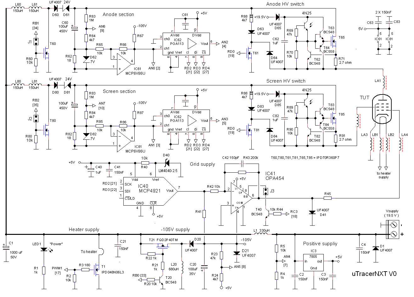
Figure 2.1 First tentative draft of the (analog part) of the uTracerNXT circuit. For this circuit diagram I used the the schematic of the uTracer6 as starting point, so component numbering may be inconsistent.
| to top of page | back to uTracer homepage |
The idea to use a Zener diode to modify the standard boost converter so that it can produce output voltages down to 0 V originates from the work on the uTracer5, a version that never made it into a fully working concept. The working is very simple, a 24 V Zener diode simply blocks the supply voltage so that when the transistor is not pulsed the output remains at zero volt. However, since the Zener diode is in the high-voltage pulse path, the question is what the penalty is in terms of efficiency.
This question was investigated using the test circuit shown in Figure 3.1., which is the boost converter stripped down to the core circuit. For the MOSFET a IPD70R360 from Infineon was used. This ōCoolMOSö device is rated at 700 V @ 300 mohm and 12 A. It has a Vt of 2.5 V so that it can be directly driven by a 5 V TTL level signal without the need for a special gate driver. In the circuit, it is driven by a 5 V pulse generator with a frequency of 10 kHz and a variable duty cycle. When S1 is closed, C1 is charged (monitored by a voltmeter, not drawn). Note, how in this circuit the UF4007 diode that in the uTracers 3 and 7 shunts the current sense resistor R2 is replaced by a Zener diode. This Zener diode has two functions. During the charging of C1 the diode is in normal forward mode, limiting the voltage drop over R2. During the actual measurement pulse, the current through C1 and R2 is reversed, resulting in a negative voltage drop across R2. R2 is selected in such a way, that in normal use this voltage drop never exceeds -5 V. However, when an excessive current is drawn, e.g. as a result of a short circuit at the output, the voltage drop across R2 can become so high that it potentially could damage the inverting OpAmp connected to R2. In these situations the Zener diode limits the voltage transient to 7.5 V, thereby protecting the OpAmp.
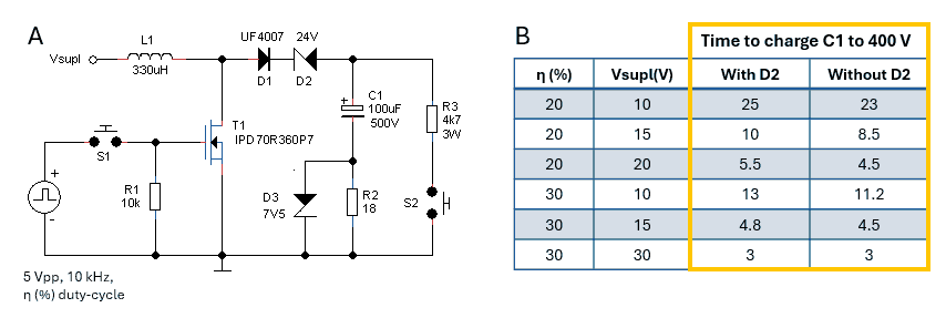
Figure 3.1 Test circuit for the zero-volt output boost converter and measurement results
The table in Fig 3.1 shows the measurement results. Measurements were carried out at 10, 15 and 20 V supply voltage and a pulse duty cycle of 20% as well as 30% corresponding to charge pulse widths of 20 and 30 us respectively. What was measured is the time it takes for the boost converter to charge C1 to 400 V with and without the 24 V Zener diode. Normally for the uTracer circuit a supply voltage of 20 V and a boost converter pulse width of 30 us is used. Note that under these conditions the difference in charging time is negligible!
As mentioned in the introduction, the OPA227 that was used in the uTracers 3 and 6 is increasingly getting difficult to obtain, especially in the DIL/DIP package. The OPA227 was originally selected for its low offset voltage (10 uV typically and 200 uV max) combined with a reasonable slew rate of 2.3 V/us. A low-cost modern alternative like the MCP6V86 offers a similar or even better performance with an offset voltage of +/- 25 uV max, combined with a slew rate of 4 V/us. However, this device is designed for a single supply voltage of 5V.
The problem is that, although these devices are advertised as having ōrail-to-railö inputs and output, the truth is that the output cannot really reach the negative or positive supply rails. The reason is that the quiescent current running through the output stage of the OpAmp always causes some voltage drop as a result of the finite on-resistance of the output MOSFETs. For the MCP6V86 for example, the datasheet specifies an ouput voltage swing of Vss + 5 mV and Vdd ¢ 5 mV. That does not seem much, but 5 mV corresponds to an error in the measured anode (or screen) current of 5 mV / 18 = 280 uA, assuming that a 18 ohm current sense resistor is used.

Figure 3.2 Simple adaptor to test the MCP6V86 in an OPA227 socket.
Browsing the internet to have a look at how others solve this problem, I ran into various interesting solutions. A very surprising find was the LM7705 which is a ōLow-Noise Negative Bias Generator,ö an integrated switched capacitor inverter that produces a -0.23 V negative supply for an OpAmp to allow its output to really swing to 0V.
A simpler solution was presented in an application note from TI entitled ōöSingle Supply Op Amp with True Drive to GND.ö The solution uses a pull-down resistor at the output of the OpAmp which is connected to a negative supply to provide a path for the output stage current to the negative supply. When the output of the OpAmp is driven to Vss (ground in this case), the output NMOS transistor in the OpAmp will now turn fully off allowing the output to swing to 0V. Of course, this requires a negative power supply, but as it happens, we very conveniently already have one in place for the negative grid supply!
To quickly test the idea, a simple adaptor was built to fit the tiny MCP6V86 into the DIL socket of an OPA227. The adaptor comprizes an LM78L05 to reduce the +15 V supply voltage to +5 V, and a pull down resistor which is connected to the -15V supply. The application note states that as a rule of thumb the output stage of an OpAmp consumes about half of the total quiescent current of an OpAmp, so for the MCP6V86 approximately 500 uA / 2 = 250 uA. For a negative supply voltage of -15 V this requires a 15 / 250 uA = 60 kohm pull doen resistor. I used a slightly lower resistance of 47 kohm. For the real circuit with a -105 V grid supply the value of these resistors (R67 and R87 Fig 3.2) will need to be increased to 105 / 250 uA = 420 kohm.
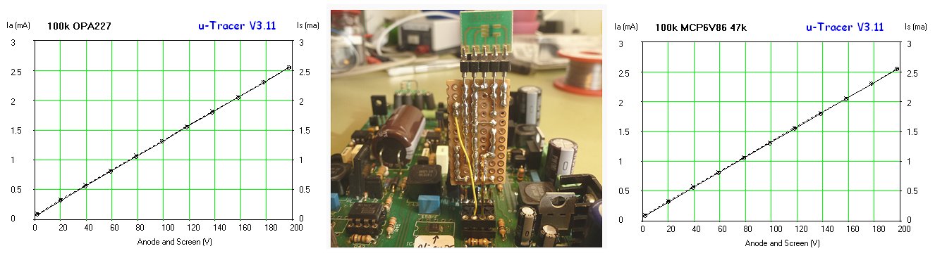
Figure 3.3 First tests with the MCP6V86 adapter in an uTracer3+.
In a first test in a uTracer3 the plugin circuit worked like a charm! Figure 3.3 shows the MCP6V86 adapter board replacing the screen OPA227 in a uTracer3+. The left graph shows a trace of two 100k resistors connected to the anode and screen outputs using the original circuit with two OPA227s, while the right graph shows the same measurement using an OPA227 for the anode section, and the MCP6V86 adaptor for the screen. Find the differences!
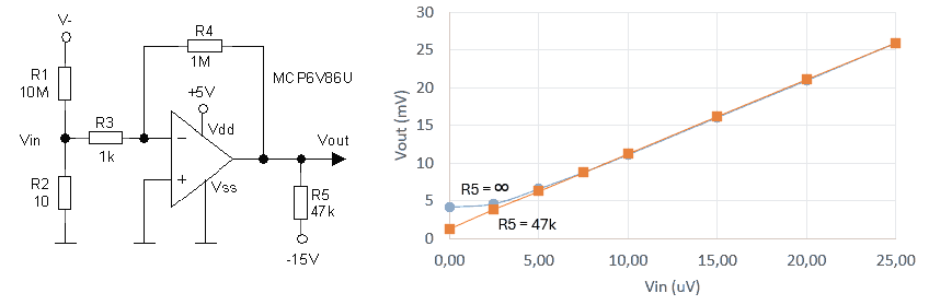
Figure 3.4 Test circuit and measurement results of the MCP6V86 for very low input voltages, with and without output pull-down resistor.
To study the offset and output-to-negative supply voltage standoff behaviour of the MCP6V86, the circuit shown in Fig. 3.4 was used. The OpAmp is configured as an inverting amplifier with a gain of -1000x. The 10 Mohm resistor basically acts as a current source to the 10 ohm resistor R2. In this way, a voltage V- = -10V will result in a input voltage of Vin = -10 uV across R2, and thus ideally in +10 mV at the output of the OpAmp. The graph in Fig. 3.4 shows the output voltage of the OpAmp as a function of input voltage Vin. The combined effect of the OpAmpÆs offset voltage and output-to-negative supply voltage standoff for this OpAmp without an output pull-down resistor at Vin = 0 V is only 4.5 mV! With the pull-down resistor of 47 kohm the output voltage at Vin = 0 V drops to 1 mV. These measurements suggest that the input referred offset voltage of this OpAmp is 1 uV, while the output standoff voltage is 3.5 mV. The datasheet of the MCP6V86 does not give a typical offset voltage only maximum values of +/- 25 uV, so for this particular device 1 uV is indeed excellent, but potentially it could be higher. The output standoff voltage of 3.5 mV is in good agreement with the datasheet.
 The high-voltage switches connect the charged 100 uF capacitors to the anode and screen terminals of the tube during the 1 ms measurement pulse in which the currents are measured. A particular design requirement of the switches is that the switches are completely floating with respect to the rest of the circuit to ensure that all the current is passed through to the current sense resistor in series with the 100 uF capacitor.
The anode and screen high-voltages switches in the uTracer3+ were based on a PNP switch design. Although it worked fine in more than 2500 uTracers, from time to time the switch tended to fail as a result of massive short circuits at the output, or violent oscillations in the tube circuit. Another point of concern is that high-voltage, high power pnp transistors are increasingly becoming obsolete, if not non-existent at all. It was the reason why the high-voltage switch circuit was completely redesigned for the uTracer6 which operates at voltages up to 1000 V. The uTracer6 high-voltage switch circuit is based on a readily available high-voltage NMOS transistor. The development of the switch circuit is extensively described in the uTracer6 weblog pages.
In the 450 or so uTracer6Æs ōin the fieldö the NMOS high-voltage has shown to be very reliable, with no failures reported to date! Reason enough for me to copy and adapt the circuit for the uTracerNXT. The principal circuit is reproduced on the left. Basically the only modification to the circuit is the replacement of the 1050 V STD2N105K5 NMOS transistor by a readily available 700 V IPD70R360 transistor made by Infineon.
| to top of page | back to uTracer homepage |
Although the grid bias section of the uTracer3 served its purpose perfectly, it is a bit of a strange circuit. In the first place because it uses as DAC one of the PWM outputs of the PIC combined with a low pass filter, and in the second place because it had to be referenced to the cathode potential, in this case basically the positive supply voltage. Furthermore, the grid voltage range was limited to 0 to -50 V, and over the years I got a lot of requests - especially from people who want to trace/test tubes like the 300B - to extend that range to (at least) -100 V.
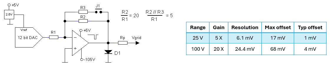
Figure 4.1 Basic idea for the uTracerNXT grid supply.
Now that I am going though a major revision of the circuit anyway, it seems like a good moment to revise the whole grid supply concept. The fact that the grid voltage is now referenced to ground instead of the supply voltage makes things a lot easier. Figure 4.1 left shows the simple plan. Simila to the uTracer6, the circuit is again based on a high-voltage OpAmp. The LTC6090 from Anaglo Devices that is used in the uTracer6 has given me quite a bit of headache. In the first place because it is sometimes difficult to source, and secondly because its price has really soared since the COVID semiconductor shortage. This time I want to bet on an OpAmp from Texas Instruments, the OPA454 with a maximum supply voltage of 100 V or perhaps even the OPA455
with a maximum supply voltage of 150 V.
The idea is to supply the OpAmp from the +5 V supply voltage and a -105 V negative supply voltage. The few volts overhead will allow for the output to comfortably swing between 0 and -100 V. The grid voltage is controlled by an SPI controlled 12 bit DAC for which I have the commonly available MCP4921 in mind in combination with an LM4040C25 2.5 V reference. Most ideal would be to have a single range of 0 to -100 V with high precision and low offset. However, although the datasheet of the OPA455 specifies a typical offset of 0.2 mV, the maximum offset is specified at 3.4 mV. With a gain of 100 / 5 = 20, an offset of 3.4 mV at the input will result in an output offset of 20 x 3.4 = 65 mV which is rather high.
It seems therefore a good idea to at least create the possibility to split the grid voltage range up in a 0 to -25 V range for general tubes, and a 0 to -100 V range for tubes like the 300B and transmitter tubes. So, using a jumper or a switch, the OpAmp can be configured as a -20X or -5X amplifier. The table in Fig. 4.1 gives for both ranges the grid voltage resolution, and both the maximum as well as the typical offset voltage to be expected. With a bit of luck, the offset voltage is low enough so that the 0 to -100 V range will suffice for most tests.
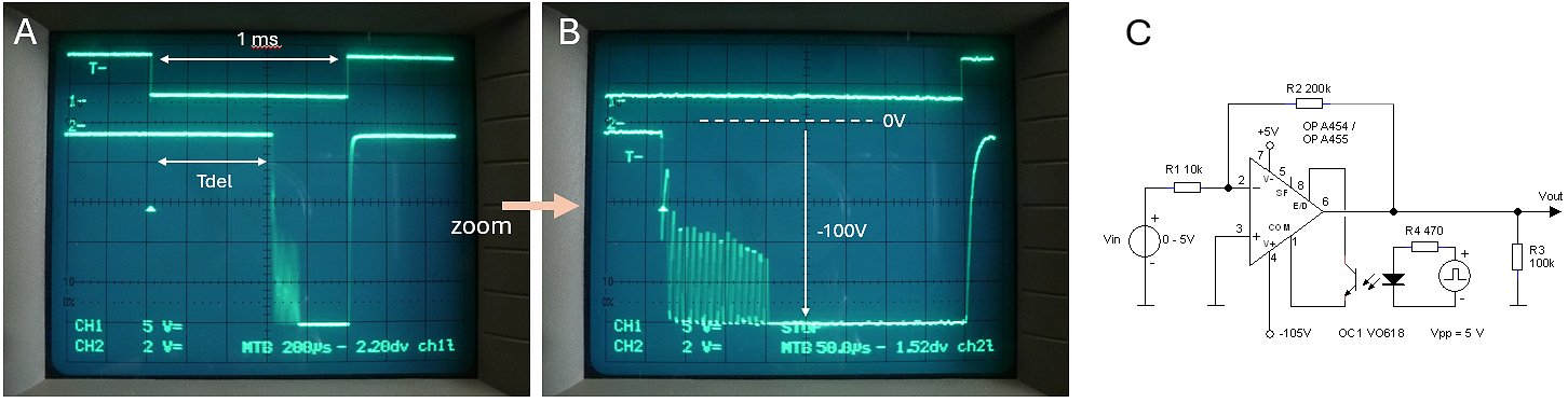
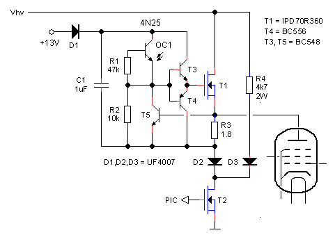
Figure 4.2 First attempt to enable / disable the OPA455 using an optocoupler. The upper trace is the signal driving the LED in the opto coupler.
When the level is low, the LED is off, and the phototransistor is not conducting.
Like in the uTracer6, the grid supply will work in pulse mode, whereby the OpAmp is only enabled during the actual measurement pulse. The main reason is to limit the dissipation in the OPA455 and thus to prevent the need to use the thermal pad of the device, which is a nightmare for simple hobbyists. This is relevant in normal operation, but especially also when the grid output is short circuited. During a short circuit or a flashover from screen or anode, the output of the circuit is protected by Rp and D1. In case of a flashover the OpAmp is protected against positive voltages by D1 while Rp limits the current. In case of a short circuit to ground Rp limits the output current of the OpAmp to a safe value of 30-40 mA. Although the OpAmp can sink that current continuously, it would cause considerable dissipation in the device. Operating the supply in pulse mode virtually eliminates this. Additionally, the resistor acts a grid stopper, reducing the chance on oscillations.
Operating the Enable / Disable (E/D) input of the OPA455 turned out to be more difficult than expected. The E/D input is referenced with respect to the E/D Com pin. A logic high on the E/D pin enables the OpAmp, a logic low disables it. A ōhighö on the E/D pin may not exceed 7 V with respect to the E/D Com pin. There is considerable freedom to define the E/D Com level, but one way or the other with the highly asymmetric supply voltages I am using here it, at least for me, it turned out to be impossible to operate the E/D pin in the conventional way with E/D Com referenced to ground. In fact, I destroyed two OPA455 OpAmps while experimenting with the circuit.
Figure 4.3 Improved Enable / Disable optocoupler drive for the OPA455.
A solution was suggested in the datasheet of the OpAmp which states ōwhen E/D Com and E/D are left open, the OpAmp is enabled, when E/D is connected to E/D Com, the OpAmp is disabled.ö Using a simple optocoupler between the two pins made it possible to connect or disconnect the two pins while leaving them completely floating with respect to the system ground (Fig. 4.2). The idea worked, but not without issues. As can be seen (Fig. 4.2 left), there is a considerable delay between the LED of the optocoupler switching off and the OpAmp switching on. Additionally, there is some oscillatory behavior as the OpAmp switches on. Both phenomena can be attributed to the low currents and thus high impedances by which both pins are internally biased.
The datasheet of the OPA455 states that the E/D Com pin can be connected to the negative power supply rail without problems and also suggest using a pull-up resistor to prevent oscillations (Figure 7-1 datasheet). Implemented these measures (Fig. 4.3) not only solved the switch-on delay, but also eliminated the oscillations.
The datasheet of the OPA455 mentiones another peculiarity of the OPA455, and that is that in disabled mode, the output impedance of device is not infinite, but around 160 kohm. This explains why in figures 4.2 and 4.3 the off-level is not exactly 0 V. For our application, this is obviously not a problem.

Readers of my pages by now know that, from time-to-time, I like to adorn my pages with personal pictures that have a special meaning to me. They remind me later when I re-read my pages I am reminded of a particular event or circumstance that occurred during the working on that page. In this case at this moment of time my wife and I are going to a rather difficult time. At the same time I am retiring, not only from Philips but also from my part-time professorship at the Technical University of Delft. In this case this picture, taken after the defense ceremony of my last PhD student acts as a ōpars pro totoö for all the changes going on in our lifes at the moment.
Download her thesis here
| to top of page | back to uTracer homepage |
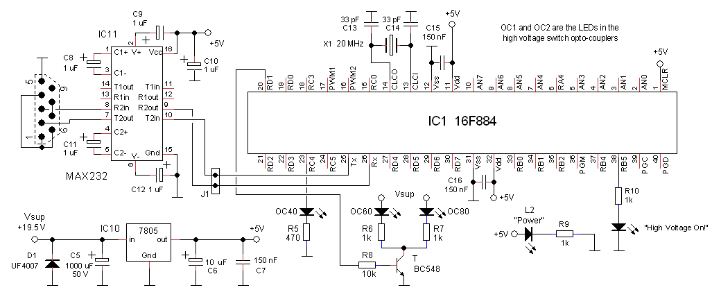
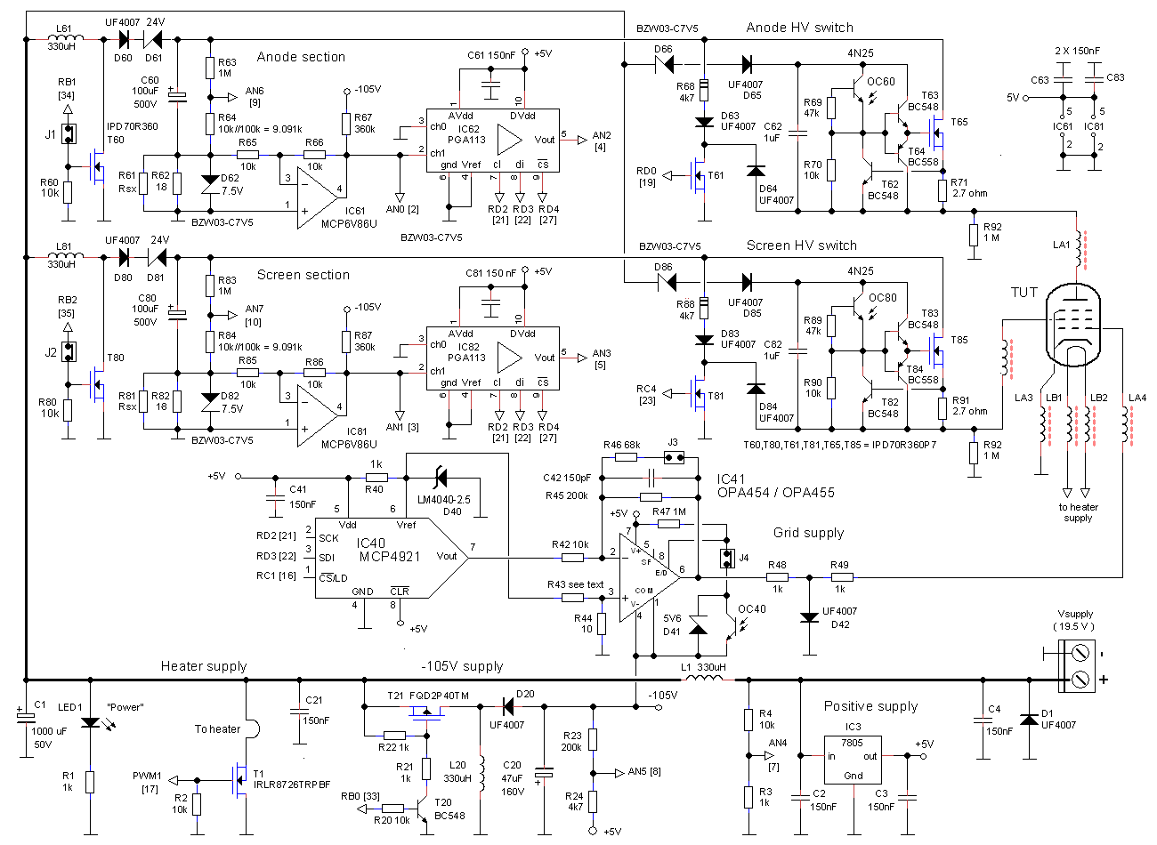
Figure 5.1 Updated schematic of the uTracerNXT
For the construction of the prototype a half populated uTracer3 PCB was married to a piece of perf-board (Fig. 5.10). Two adapter PCBÆs were used to fit the MCP6V86U OpAmps into the OPA227 sockets. New is the vertical mounting of the inductors (mis)using modified pin headers. It appeared that the normal mounting of the inductors sometimes results in some bad connections because people find it difficult to solder them. In this way that problem is solved, and I think I will also implement this method in the final kit. For the prototype I used two of the 100 uF / 500 V capacitors that are also used in the uTracer6. This allows me to go to 500V anode and screen bias. Two ZIF sockets were used for both the MCP4921 DAC as well as the OPA455 high-voltage OpAmp. This makes it very easy to test different components e.g. to look at the spread in offset voltages etc.
In the uTracer3 both the ōpower-on LEDö as well as the ōHV-LEDö were fed from the +5V supply using a 180 ohm resistor resulting in a current of 20 mA / LED, almost 6 times the current consumption of the PIC! By powering these LEDs directly from the +19.5 V supply, the current consumption on the +5V is so much reduced that the heatsink can be eliminated. Quite a large number of jumpers were used to be able to isolate certain circuits parts in this evaluation phase. Although the circuit looks quite large, I am sure that when all the adapter PCBÆs, jumpers etc. are omitted the complete circuit will easily fit on a PCB with the same size as used for the uTracer3.
To reduce the charging time for the higher anode and screen voltages of 500 V, the charge pulse width for the high-voltage boost converters was increased. According to the datasheet of the 330 uH inductors, they saturate at a current of 2 A. At that current the inductance, by the way, is already reduced to 70%. The current I through an inductor L for an applied constant voltage V for time t is given by: I = (V*t)/L. So the time needed to reach a current I is given by t = (I*L)/V. For V = 20 V, I = 2 A, L = 330 uH, we find t = 33 us. To be a bit on the safe side, the boost converter pulse width was increased to from the 24 us that was used in the uTracer3 to 29 us in the new design. This reduced the time to charge the 100 uF capacitors to 500 V from 9 to 4.5 seconds.
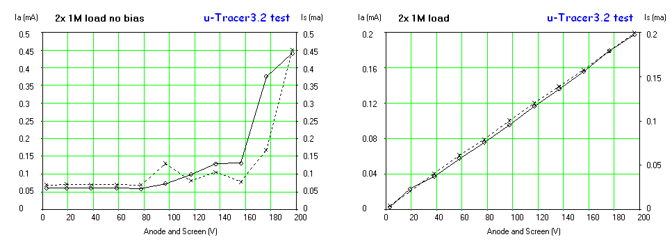
Figure 5.2 Low current performance without (left) and with (right) the OpAmp output pull-down resistors.
Figure 5.2 shows the necessity of the pull-down resistors at the output of the current sense OpAmps. Without the resistors basically no current measurements below 500 uA are possible. The pull-down resistors of 330k connected to the -105 V negative supply rail provide a near ideal current sink of 105V / 330 k = 320 uA, resulting in a near linear operation down to 10 uA.
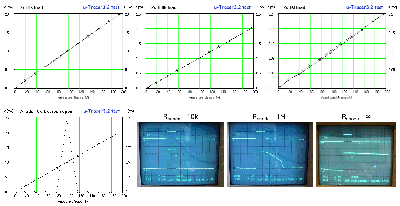
Figure 5.3 Top: anode and screen current measurements over three decades using a 18 ohm current sense resistor.
Bottom: anomalies observed with open output.
Figure 5.3 illustrates the anode and screen current measurement performance over three decades of current from 200 mA down to the tens of microamps range using an 18 ohm sense resistor. From experience with the uTracer3 this is a practical range for most common tubes. It is always possible to reduce the value of the current sense resistor should higher currents be necessary, of course at the expense of a somewhat noisier performance at the low current end range. Read more here and here.
By accident I observed an anomaly when the anode terminal of the circuit was connected to a load (resistor), while the other was left open, or visa versa. The left-bottom graph of Fig. 5.3 shows how suddenly at a certain voltage the screen current jumps to some high value and then return to zero again. It was found that even with the tiny load of a 1 M resistor connected to the screen terminal the behavior was normal again. The origin of the phenomenon was traced back to the discharging of the high-voltage switching circuit. Observe that the whole high-voltage switch circuit is electrically floating, and that its potential moves up and down with the output voltage. When suddenly the output transistor opens, the whole circuit has to discharge through the load at the output. The three scope traces in Fig. 5.3 show on the upper channel the measurement pulse issued by the PIC and on the lower trace the screen output voltage, and that for three different loads. With a 10 k resistor connected to the screen terminal, the width of the output pulse is identical to the measurement pulse as issued by the PIC. So, the 10 k resistor discharges the high-voltage switch circuit very fast. With a 1 M resistor connected to the screen terminal we see that it takes some time for the output voltage to reach zero. With an estimated time constant of approximately 3 ms this leads to the conclusion that the effective capacitance of the high-voltage switch circuit to ground is in the order of 3 nF. With no load connected apart from the 10 M resistance of the 10:1 scope probe the discharge time becomes even larger. It is obvious to assume that with no load at all, the output is still charged before the next measurement pulse is issued.
The issue can easily be remedied by permanently connecting a 1 M load resistor between the output and ground. Obviously, this will increase the output current, but since both the output voltage as well as the resistance value are known, this additional current can easily be compensated for by the software in the GUI.

Figure 5.4 Offsets in the grid bias circuit.
The idea behind the control grid supply circuit is very simple (see figure 4.0). A 12 bit DAC provides a programmable voltage between 0 and 5 V. Then a -20x amplifier converts this into a 0 to -100 V voltage. Unfortunately, the situation is not as simple as that due to non-idealities in especially the DAC and the high-voltage OpAmp. First of all, although the DAC is claimed to be ōrail-to-rail,ö as explained in the previous section, this in practice means ōalmost rail-to-rail.ö For a programmed 0 V output voltage, in practice the output voltage will saturate to a finite value, which according to the datasheet (Fig. 5.5) can be as high as 10 mV. Although this is not really an offset voltage, nevertheless in Fig. 5.4 this is represented by an offset voltage Vo1. Additionally, the high-voltage OpAmp can have an offset voltage which, according to the datasheet (Fig. 5.5) can vary between +/- 3.4 mV, although the statistical distribution graph from the same datasheet shows that in practice the offset voltage will be much smaller. The equation in Fig. 5.4 shows how these two offset voltages result in grid voltage offsets varying between -270 mV and +71 mV, which is unacceptable for accurate measurements on tubes e.g. like the ECC83.

Figure 5.5 Measured offsets in the DACs, OpAmps and the complete circuit; and excerpts from the data sheets of the MCP4921 and OPA455.
The get a feeling of the extent of the problem, I did some measurements using the prototype setup with two OPA455 OpAmps on adapter PCBs and eight MCP4921 DACs: one SMD version and 7 DIL packaged devices (Fig. 5.5 left). For these measurements, the gain of the OpAmp was set to -20x. For the first set of measurements the DAC was removed from the ZIF socket and the input of the OpAmp amplifier circuit was connected to ground, and the output voltages for the two OpAmps were measured indicating offset voltages of: OpAmp1 -19.8 mV / -20 = +0.99 mV, OpAmp2 -7.4 mV / -20 = +0.37 mV. Next the DACs were inserted and both the DAC output voltage, as well as the amplifier output voltages were measured. Most DACs exhibited a low ōoffsetö voltage of 1.2 mV, however, there was one ōbad boyö with an offset of 7.3 mV which, by the way, is still within specifications. It is gratifying to see that the resultant OpAmp output voltages closely follow the theory.

Figure 5.6 Principle of offset correction in the uTracerNXT.
If the resultant offset voltage at the output of the OpAmp is positive, then it can be simply compensated for in software by defining a new nÆ(Vgrid) = n(Vgrid) + ncorr, or in other words ōshifting the y-axis.ö However, as we have seen, it is more likely that the resultant offset at the output of the OpAmp is negative. Figure 5.6B shows this situation. In this case, it is not directly possible to compensate for the offset in software. A solution is to ōshiftö the entire curve up, so that the offset becomes zero or even positive. The equation in Fig. 5.4 suggests how this can be done. Introducing a deliberate positive Vo2 will shift the curve upwards. The schematic in Fig. 5.1 shows how this is implemented in the uTracerNXT. A relatively large resistor R43 connected to the 2.5 V reference voltage bleeds a small current through the 10 ohm resistor R44 causing a deliberate positive offset shift. As an example for R43 = 10 k, the shift at the input is 2.5 mV; with a gain of 20x this results in an offset voltage at the output of the OpAmp of 50 mV.
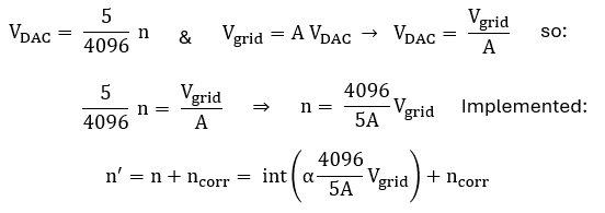
Figure 5.7 Implementation of the control of the grid supply in the GUI.

Figure 5.8 Measured offsets after calibration over the full control grid bias range.
So, how well does all this work out in practice? Figure 5.8 shows the result of the grid bias circuit evaluation using a DAC with a low-offset (left) and the DAC with a high-offset, the bad-boy (right). Looking at the low-offset DAC, we see that the initial offset was -11.5 mV. Using a 10k resistor for R43 this was lifted to +12.1 mV. For a gain of 20 (the zero to -100 V range) the grid voltage in the GUI was set to the mid-range value Vgrid = -50 V. Next the slope correction factor α was adjusted so that the measured Vgrid was -50 V. Next, the grid voltage was set to a very low value - I used -200 mV - and ncorr was set to such a value that the measured grid voltage was as close to -200 mV as possible. After the calibration the grid voltages for set point values between zero and -100 V were measured and the error recorded. The same procedure was repeated for the zero to -25 V grid bias range. Finally, the high-offset DAC was evaluated in the same way.
We observe that over two orders of magnitude from Vgrid = -1 V to -100 V the deviation in the grid voltage is less than 1%. Below -1 V the error increases with a maximum of around 3%, from the graphs in Fig. 5.8 this looks more serious than it is. Note that a few percent deviation is hardly something to worry over in ōtube world.ö Also note that after calibration the high-offset DAC performed even slightly better that the other one. I think that with more careful calibration, e.g. by using a different test voltage for the ōncorr calibration stepö, the overall accuracy can still be improved. All in all, I am quite satisfied with the performance of this simple and cost-effective circuit!
Firmware and GUI updates
Both in the firmware as well as in the GUI a number of changes and updates have been made. Whereas the changes in the GUI are limited to the way the different voltages are calculated, in particular taking into account that anode, screen and grid voltages are now referenced to ground. The changes in the firmware are more substantial, and in part very similar to changes implemented in the uTracer6:
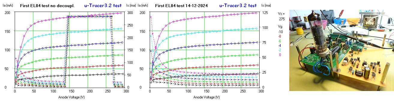
Figure 5.9 First tube measurements with the uTracerNXT
With the control grid section in place and calibrated, it was time for the first tube measurements. Test vehicle was of course my trusted EL84 (Fig. 5.9). To my surprise and disappointment, the same strange phenomenon observed in Fig. 5.3 returned! Suddenly, the screen current jumps up to the maximum value, to return to normal values for higher voltages (Fig. 5.9 left). After a lot of searching, I concluded that there was nothing wrong in the signal path to the point of the PGA input, so that the fault had to be related to the PGA113. Could it be that noise on the +5V supply to the PGA caused it to behave in a strange way? Indeed, a small 47 uF capacitor placed directly over the supply terminals of the PGA113 solved the problem completely (Fig. 5.9 middle). Obviously, the ad hoc wiring of the prototype is far from ideal and most probably the root cause of this hiccup. Anyway, something to keep in mind for the final PCB layout.

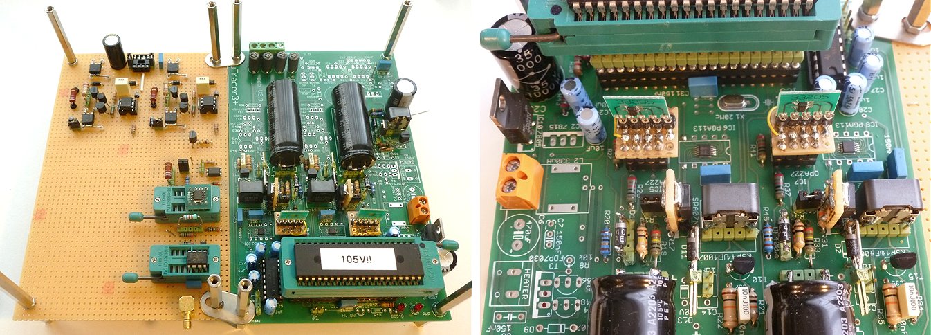
Figure 5.10 uTracerNXT prototype
| to top of page | back to uTracer homepage |

Readers of my weblogs will have noticed that from time to time, I like to include some personal mementos in my pages to remind me of special moments in my life that occurred during the working on my projects and the writing of these pages. So also this nice picture of some colleagues and most of my former PhD students. The first of August 2024 after 36 years I officially retired from Philips Research. Due to a variety of personal reasons, most of them not so pleasant, we never came around organizing an official farewell party. It was therefore a huge surprise when a large group of my former students organized a surprise party for me! They lured me under some pretense to suitable location in Eindhoven where we had a fantastic party! It was the best farewell party I could have wished for!
| to top of page | back to uTracer homepage |
The heater supply for the uTracer3 was originally designed as a simple and cheap add-on circuit that conveniently made use of one of the unused PWM outputs of the processor. Much has been said and written about its accuracy. Its main Achillis heel was that the PWM operated at a high frequency of 19.5 kHz. As a result, any (parasitic) inductance in the heater wiring markedly lowered the effective power delivered to the filament (read more here). For this reason, many users of the uTracer opted to add an external heater supply, often provided with a digital voltage and current readout. For the uTracer6 I decided to use the same circuit idea, be it operating at a much lower frequency, which greatly improved the accuracy. Although I could have gone for a much more elaborate heater circuit, this really doesnÆt make much sense. As explained in the uTracer6 Weblog, there are so many cheap and excellent ready-made alternatives on the market, that I can never compete with those.
A change with respect to both the uTracer3 as well as the uTracer6 is that in the uTracerNXT the cathode is referenced to ground instead of to the positive power supply voltage. This implies that whereas previously the heater was simply connected to the positive supply voltage and driven by a single NMOS transistor, in the uTracerNXT - to accommodate directly heated tubes - the heater on one side must be connected to ground, so that it needs to be driven by a ōhigh-sideö PMOS device. This makes the circuit a little bit more intricate.
Directly heated tubes have the tendency to draw a lot of heater current at low voltages. Especially transmitter tubes can easily consume many amps of heater current at only a few volts. These high currents are obviously out of reach for the internal heater supply of any uTracer. So to test these tubes an external power supply is needed. For the uTracer3 this required the use of a DC power supply, because an AC supply would interfere with the accurate setting of the grid voltage, introducing noise in the measurements. For the uTracer6 extension board a simple add-on was developed to be able to use an AC heater source ¢ a transformer ¢ by synchronizing the measurement pulse with the AC voltage. For the uTracerNXT I decided to include the same option, so that it is now possible to accurately measure tubes like the 300B (5 V @ 1.2 A), 2A3 (2.5 V @ 2.5 A), 812A (6.3 V @ 4 A), etc. using an external transformer as heater supply.
Referencing the heater supply to ground
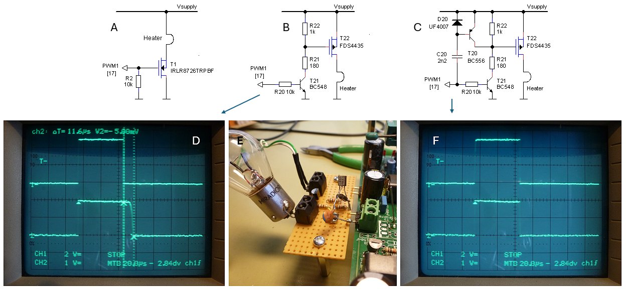
Figure 6.1 Heater circuit variations. The upper traces in the scope pictures are, top: the PWM input signal (2 V / div), bottom the heater voltage (10 V / div).
Referencing the heater to ground at first sight seemed rather straightforward, a suitable PMOS transistor connected to the supply voltage with a low-side npn transistor driving the gate (Fig. 6.1B). However, on testing it, the trusted 6.3V lamp I always use to test the heater supply burned much brighter that I was used to. What I had overlooked was that the high current PMOS has about 6 times the gate capacitance compared to the high-voltage PMOS transistors I usually use in the negative power supply boost converters. So, for the 1k resistor it takes about 11.6 us to switch off the transistor (Fig. 6.1D).
How serious is that? Remember that the PWM duty cycle is given by η = (Vh / Vsupl)^2, with Vh the set heater voltage and Vsupl the supply voltage. In the measurement shown in Fig. 6.1, the heater voltage was set to 5 V. So with Vsupl = 20 V and a PWM frequency of 1.2 kHz, the nominal PWM pulse width needs to be 51.2 us. Extending the PWM pulse to 62 us will result in an apparent heater voltage of 5.5 V. So where in the past when we were bitten by parasitic inductances the effective supply voltage of the heater was too-low, now it is too high!
Fortunately, there was a simple remedy for the problem (Fig. 6.1C). During the rising edge of the input PWM signal, C20 is discharged (or charged is you like), through diode D29. Then, at the trailing edge of the PWM signal, the inertia of the capacitor ōpulls-downö the base of T20, causing it to conduct, thereby quickly discharging the gate of T22. The bottom trace of Fig. 6.1F shows the improvement. The circuit trick worked so well that I also used it for the negative power supply.
AC heater supply synchronization for DHTs
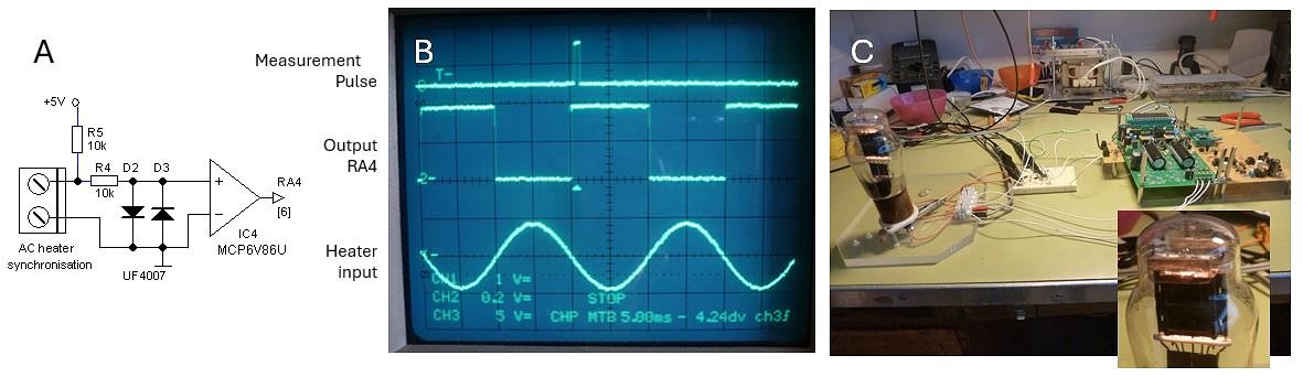
Figure 6.2 A: Zero-crossing detector, B: The AC heater synchronization circuit in action. Note how the measurement pulse (upper trace) practically coincides with the zero-crossing of the AC heater voltage, C: Test-setup around a 10Y DHT.
To allow for an AC heater supply for DHT tubes, the timing of the measurement pulse needs to be synchronized with the AC heater voltage, preferably in such a way that the moment of measurement coincides with the zero crossings of the heater voltage. For the zero-crossing detector several ōone transistor typeö circuits were considered, but in the end, I opted for the circuit depicted in Fig. 6.2. In the circuit the MCP6V86 OpAmp is misused as a comparator. The AC heater voltage is fed via current limiting resistor R4 to the input of the OpAmp, while diodes D2 and D3 limit the voltage to +/- 0.6 V. To prevent random toggling of the output in the absence of an input signal, resistor R5 pulls-up the input voltage so that the output of the OpAmp becomes permanently high.
A very small piece of code was added, which just before the grid bias is enabled and the measurement pulse is issued, checks input pin RA4 to wait for a 0->1 transition. When a transition is found, the routine exits and a measurement follows. In case no transition is found in 24 ms, there is apparently no AC signal present and a measurement follows anyway (see pseudo code below).
CNT := 140
AC_OLD := portA.4
do forever
delay 0.1534 ms
CNT := CNT ¢ 1
if CNT = 0 then return æno 0->1 transition found
if portA.4 = 1 then
if AC_OLD = 0 then return æ0->1 transition found
else
AC_OLD := 0
end if
end do
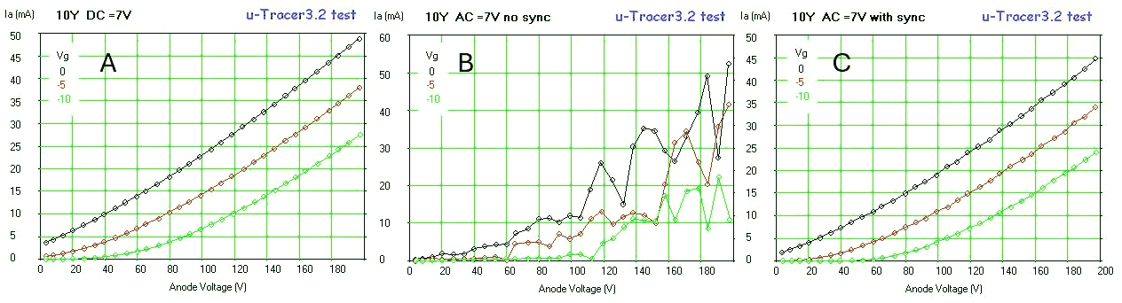
Figure 6.3 Set of curves taken from the 10Y DHT with heater, A: Fed from a 7 V DC source, B: Fed from a 7 V AC transformer without synchronization, C: The same with synchronization.
Figure 6.2C shows the test-setup used to test the heater synchronization circuit and firmware. It turned out that an old 10Y triode was one of the few, if not the only DHT tube I have apart from some very heavy-duty transmitter tubes. The traces in Fig. 6.2B show the synchronization circuit in action. The upper trace shows the measurement pulse which is used to trigger the scope (note that in this case a 0.5 ms measurement pulse was used). The lower trace is the AC voltage applied to the heater, while the middle trace depicts the output signal of the zero-crossing detector circuit. Note that there is a tiny 0.5 ms delay between the zero-crossing and the measurement pulse which is caused by a short software delay inserted to stabilize the tube between the moments the grid voltage and the anode/screen voltages are applied.
Figure 6.3 shows the effect of the heater synchronization. Figure 6.3A shows a set of output curves taken from the 10Y using a DC 7V heater supply. In Fig. 6.3B a 7 V transformer is used to power the heater without any synchronization. Because the moment of the measurement pulse is now completely random with respect to the AC voltage, the effective grid voltage varies drastically from point to point, resulting in very noisy curves. In Fig. 6.3C again a transformer is used, but now the synchronization circuit is connected to the heater. Note, that there is a (small) difference between the current values using the DC heater power supply and the transformer. This is caused by the fact that in the case of the synchronization circuit, the complete heater filament is at 0 V, while in the case of the DC heater supply the 7 V heater voltage is distributed over the filament, resulting in a slightly higher (more positive) effective grid voltage (see also Fig. 15-4 here).
For another example of a measurement of a directly heated tube with the heater powered by a transformer have a look at this trace of a very nice ō45ö tube.
Something that has nothing to do with the uTracerNXT: some snapshots of my Tektronix 577 that my friend (and former colleague) Peter Blanken and I recently brought back to life. The first 20 years or so of my career at Philips Research, I worked extensively with a Tektronix curve tracer, be it the model 576. I have always missed one at home for quickly checking transistors and diodes. Luckily, sometime ago I was able to buy this more modern version 577 from our test equipment department for scrap-metal price. It needed some restauration but now it is fully functional again and has already shown its value during the repair of broken uTracers.
| to top of page | back to uTracer homepage |
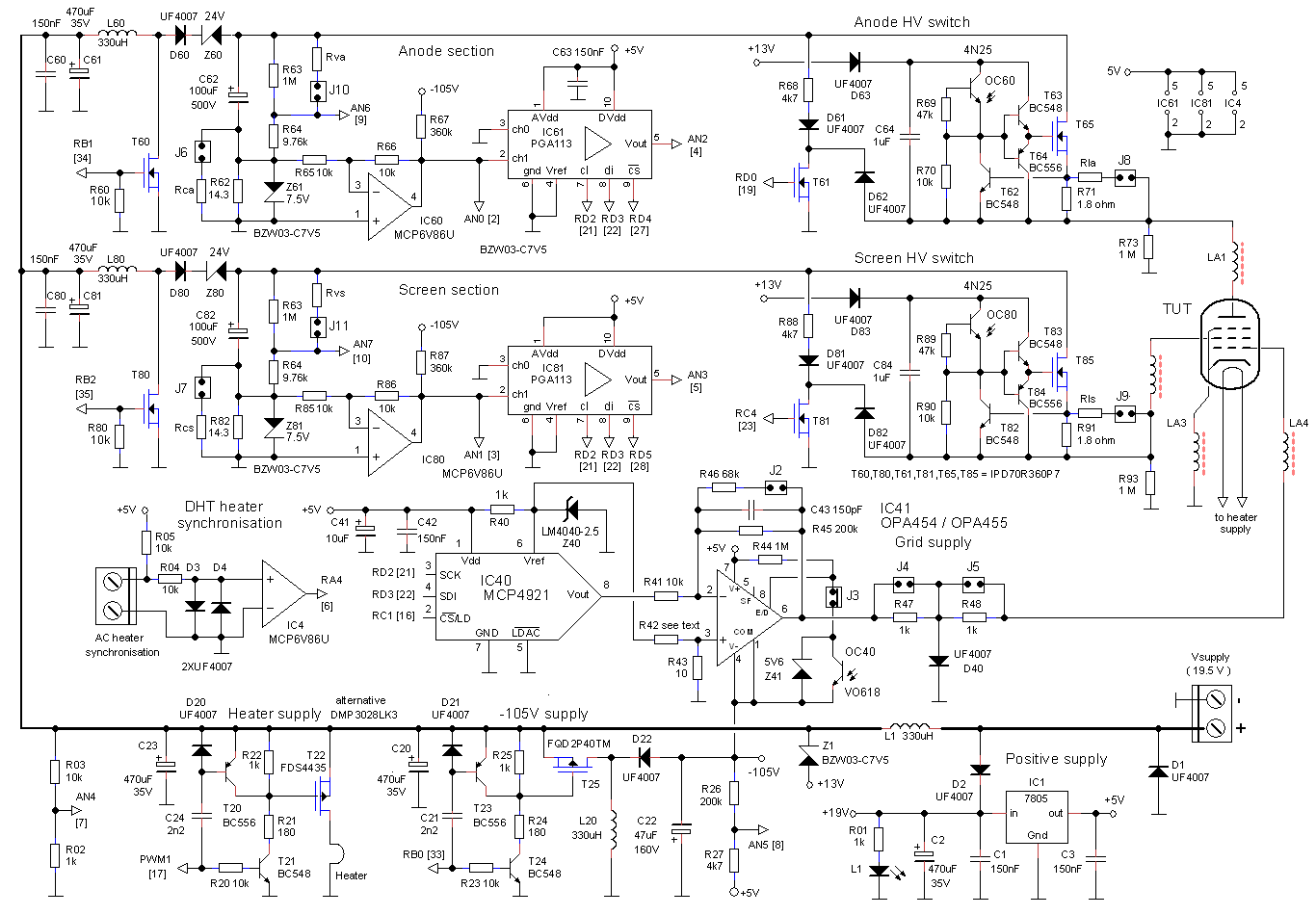
Figure 7.1 Schematics (with some small changes) as they were used for Version 0 of the PCB for the uTracerNXT.
Figure 7.1 shows the schematics of the uTracerNXT as it was used for Version 0 of the PCB including some small modifications to include the selectable voltage ranges and with some renaming of components. Note that this is still a test version and that the schematics may still change during the development of the device.
Since the uTracerNXT is meant as a drop-in replacement of the uTracer3, the dimensions of the PCB and the locations of the drillholes were not changed. Also, the location of the power, heater and electrode terminals remained (more or less) the same. The only exception is the addition of a terminal block for the AC heater synchronization circuit.
Figure 7.2 shows the PCB and the location of the different circuit parts. The layout of the PCB was a bit of a puzzle. First of all because there are quite a few components that all have to find their place. Next, some parts of the circuit carry a high-voltage, so that sufficient clearance to low voltage parts has to be taken into account. In some parts of the circuit, especially the boost converters, there are high (peak) currents flowing. These circuits parts have been provided with local 470 uF and 150 nF decoupling capacitors. Additionally, the areas enclosed by high current loops were kept as small as possible to minimize RFI radiation. Finally, there is the point of aesthetics; to satisfy my autistic urges I tried to make the layout as symmetrical as possible.
The high-voltage switches as well as the grid supply sections were provided with locations where additional resistors can be placed to modify current and grid bias ranges. In the build shown on Fig. 7.2, these locations are provided with modified pin-headers to facilitate quick and easy changing of resistors. The ranges can be selected by placing the appropriate jumpers. In the meantime, I also decided to add jumpers and resistor locations so that the anode and screen voltages ranges can be modified. These will be incorporated in a next version of the PCB.
Apart from a few text typos and some drill holes that were on the small side, the PCB worked first time without any layout issues. This is not a mean feat, since my version of Eagle only supports ōpolygon pushingö and no layout entry of layout versus schematic checking! As mentioned, this is just the first version of the PCB, and both the schematics and thus obviously also the PCB may be subject to changes.
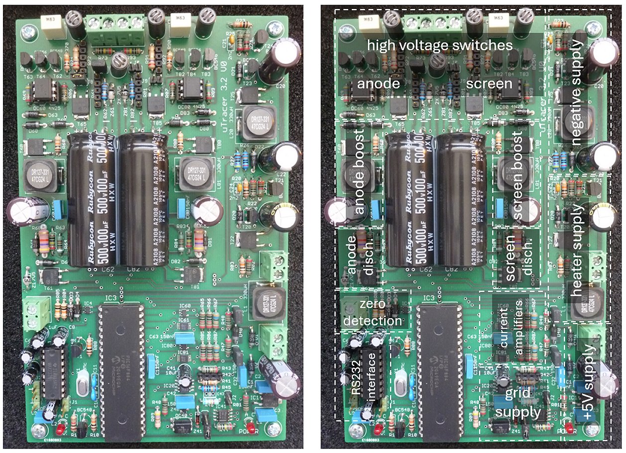
Figure 7.2 Version 0 of the uTracerNXT.
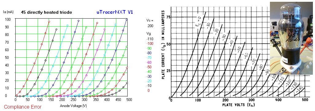
Figure 7.3 A nice illustration of the capabilities of the uTracerNXT, a set of characteristics of the among audiophiles well known 45 tube (left). On the right the same set of curves from the Tung-Sol datasheet. In this case the heater was powered by a transformer, making use of the new feature of the uTracerNXT to AC power directly heated tubes (see Section 6). For this measurement I set the compliance to 100 mA, to not unnecessarily push the current beyond that limit. Of course, the notice ōCompliance Errorö is not really an error, but a message that the uTracerNXT has skipped measuring the points above the set compliance value (100 mA). To speed up the measurement the range for the screen channel, which is of course not used, was set to maximum, avoiding unnecessary averages.
| to top of page | back to uTracer homepage |
The command and result strings.
The communication with the uTracer is via a serial RS232 link at a speed of 9600 baud, 8 bits, no parity, and one stop bit. The commands to the uTracer are given in the form of a string of 28 (Uppercase) ASCII characters. Each character sent to the uTracer is immediately echoed by the uTracer. Failure to echo a character is by the GUI interpreted as a malfunction of the uTracer.
Every two consecutive characters in the ASCII string represent an eight bit byte. The first byte is the command code. The following 8 bytes represent data. Different formats for the data are used depending on the command code, however in most cases the eight bytes are grouped into four 16 bit words representing the anode voltage, the screen voltage, the grid voltage and the heater voltage (Fig. 8.1).
Some strings do not result in a response from the uTracer. Other strings result in the uTracer sending a result string. The result string also has a fixed format, and consists of 38 ASCII characters. Again every two consecutive characters in the ASCII string represent an eight bit byte.
The first byte is the status byte which signals if the command to which the result string was a response was executed successfully. The remaining 18 bytes represent data grouped into 9 two byte words. The format of the result string is fixed (Fig. 8.2).
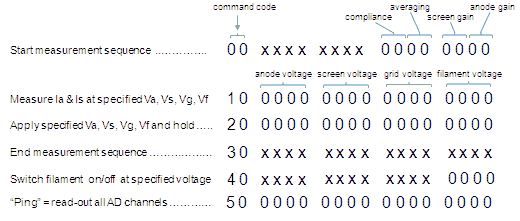
Figure 8.1 Definition of the command strings.
The data in both the command string as well as in the result string is always in 10 bits binary format. This means that the upper 6 bits of the data word are not used. These bits should be zero. In most cases the binary data directly represents a 10 bit result of the on-chip AD converter, or a setting of the 10 bit on-chip PWM modulator. All conversion of for the user meaningful numbers to and fro binary representations is done in the GUI. In this way a minimum amount of intelligence is needed in the micro-controller.
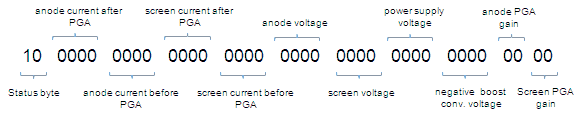
Figure 8.2 Structure of the result string
Structure of a complete measurement sequence
The different commands should be sent in a certain order, although sending the commands in a random order will not result in an error. The preferred command sequence is shown in Fig. 8.3. When the ōHeater Onö command is pressed, the GUI sends a ōSet Settingsö (<00>) command followed by a ōPingö (<50>) command to obtain the current supply voltage. It then sends the ōSwitch On Heaterö (<40>) command. The only thing this command does is to copy the last word of this command to the heater PWM generator. The other words should be ō0000ö. The heater
voltage can be directly set to the final value or the GUI can generate a ōsoft-startupö by issuing a sequence of <40> commands with increasing heater voltage values. The uTracer does not send a response after receiving a <40> command
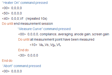
Figure 8.3 Structure of a typical Measurement Session
While the heater is heating, the user has the time to select a measurement type on the GUI and to set the proper measurement conditions. When next the user presses the ōMeasure Curveö button, the sequence to measure a set of curves is started. The first command issued is the <00> ōSend Settingsö command. This command transfers the gain settings for the anode and screen amplifiers, the required number of average measurements and the current compliance value. There is no response of the uTracer to the <00> command. Next, the GUI starts issuing <10> ōDo Measurementö commands. The four words in the command exactly specify the anode, screen, grid and heater voltages. After reception of the command, the uTracer sets all the specified bias conditions and performs the measurement. The result is communicated back to the uTracer via a result string. The value of the status byte indicates if the measurement was successful. If the status byte = 10H everything is ok, a value of 11H indicates a compliance issue on one of the two channels. The GUI can issue any number of <10> commands. At the end of a measurement sequence the GUI issues the <30> ōEnd Measurementö command. This command discharges the high-voltage buffer capacitors and sets the grid voltage to zero. In the same measurement session, more curves or a different type of curve can be measured by repeating the <00>,<10><10><10>ģ.,<30> sequence. At the end of the session the heater voltage is switched off by issuing a <40> command with a specified heater voltage of zero volt.
The format of the variables
In this section the format of the variables that are used in the communication with the uTracer will be defined. Some of these variables are one byte, while other variables use two bytes (a word).
anode and screen gain
The anode and screen gain variable is only one byte long, and used both in the <00> command string, as well as in the result string. In the command string it is used to specify the gain of the anode or screen current amplifiers, or to specify that the ōauto gain/rangeö option is selected. In the return string the variable returns the actual gain as it was determined by the ōauto rangeö algorithm in the uTracer and used for the current measurement point. The lower nibble directly reflects the gain convention as it is used by the PGA113: 00H=1X, 01H=2X, 02H=5X, 03H=10X, 04H=20X, 05H=50X, 06H=100X, 07H=200X. In additional code 08H is used to indicate that the auto-gain algorithm must be used.
averaging
The average variable is one byte long. The variable is only used in the <00> command string. In principle the variable can have any value in between 1 and 32 (001H and 20H). In practice only the values 1, 2, 4, 8, 16 and 32 are used. This is because the user can only choose from these values. When the variable has the value 40H it indicates that the auto-averaging algorithm has to be used
compliance
The compliance variable is one byte long and only used in the <00> string. The variable defines the voltage of the on-chip voltage reference which is compared by the two on-chip comparators to the voltage drop over the current sense resistors. When the voltage drop over these resistors exceeds the reference voltage, the measurement is aborted. The value of the compliance variable is directly copied into the CPU register which controls the voltage reference: VRCON.
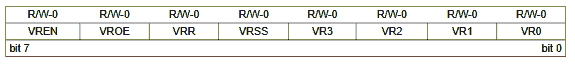
Figure 8.4 The voltage reference source control register taken from the 16F844 datasheet.
Since the voltage reference has to be enabled (VREN=1) and disconnected from the output pins (VROE=0), the highest two bits of the variable always have to be 10xxxxxx. VRR defines the measurement range while the lowest nibble of the variable selects the tap in the resistive ladder network. See also Section 9 (ōRanges&Calibration), in particular Fig. 9.1.
anode and screen voltages
The anode and screen voltages are assumed to be equal to the voltage of the 100 uF reservoir capacitors. The voltage of these buffer capacitors is measured using a resistive voltage divider so that in the default configuration the 0-500 V range is mapped onto a 0-5 V range compatible with the ADC of the PIC. As will be explained in Section 9, the user has the possibility to specify a second (smaller) voltage range by adding a resistor in parallel to resistor R2. In the GUI the resultant resistance is then used for R2.
Note that there are now two ways to calibrate the high-voltage anode and screen ranges! If the default configuration is used, the user can - just as in the uTracer3 - use the appropriate slider which directly modifies variable CalVar between 0.9 and 1.1. Alternatively, if the user is also using a personalized voltage range, the slider should be set to its middle position (CalVar = 1) and the calibration should be done by directly modifying the value of R2.
The conversion formulas which give the relation between variable n and the anode/screen voltage(s) are:
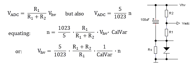
These formulas are used for both the setting of the anode and screen voltages, as well as for reading the actual voltages directly after the measurement pulse. Here we must make a small correction for the fact that the actual voltages during the measurement pulse are slightly lower than after the measurement pulse because of the voltage drop the anode or screen currents cause over the current sense resistor. So, the value of the anode / screen voltages stored is:
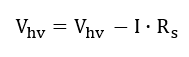
The anode and screen voltages variables occupy two words and are used both in the command as well as in the result string. Since a 10 bit AD converter is used, only the lower 10 bits of the two bytes are used. The variable n in in these equations is always clipped to 1023. Extensive information on the personalization of the anode/screen voltage ranges and the calibration procedure is given in the My-uTracer Section.
anode and screen currents
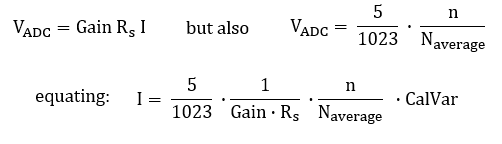
The anode and screen currents are determined from the voltage drop they cause over current sense resistor Rs (see picture above). If needed, the voltage drop is first amplified by a Programmable Gain Amplifier (PGA113) before being fed into the AD converter. When an averaging greater than 1x is used, the uTracer simply adds the consecutive measurements (ADC values) to the variable which is transferred to the GUI. The GUI subsequently performs the floating-point division. The relation between the variable n, and the anode/screen currents (in Amps) is given by:
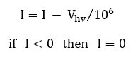
To make sure that the anode and screen outputs discharge properly after the measurement pulse a minimum load of 1 Mohm is used (see Section 5). Since the output voltage is known, the measured current is corrected for the current through this resistor. Since, due to small errors this can result in a slightly negative current, a negative current is always set to zero:
The anode and screen current variables occupy two words and are only used in the result string. Although only a 10 bit AD converter is used, the variable can use the full two-byte word of 16 bits for 32x averages. Two values which are also returned are the anode and screen currents before the PGA. In other words, the voltage directly over the current sense resistors (after inversion). This value is not used by the GUI. The conversion formulas are identical to the equations above with Gain=1 and Average=1.
In the default configuration a current sense resistor of 14.3 ohm is used corresponding to a maximum current range of 350 mA (see Section 9). As explained there, the user has the possibility to personalize (increase) the current range by adding a resistor in parallel to Rs. In the GUI the resultant resistance is then used for Rs. Note that just as for the voltage ranges, there are now two ways to calibrate the anode and screen current ranges! If the default configuration is used, the user can - just as in the uTracer3 - use the appropriate slider which directly modifies the variable CalVar between 0.9 and 1.1. Alternatively, if the user is also using the extended current range, the slider should be set to its middle position (CalVar = 1) and the calibration should be done by directly modifying the values of Rs. Extensive information on the personalization of the current ranges is given in the My-uTracer Section.
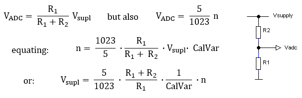
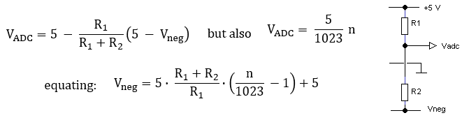
power supply voltage
The power supply voltage is measured because it is an important parameter in the calculation of the settings for the proper heater voltage. It is only used in the return string. Like the high-voltages, the power supply voltage is measured using a simple resistive voltage divider R1 and R2. Referring to the equations and figure below R1 = 1 kohm and R2 = 10 kohm.
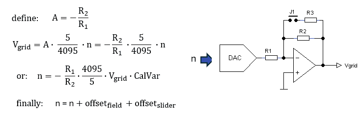
control grid voltage
The control grid voltage is always negative with respect to the cathode, which is at ground potential. The control grid bias circuit is driven by the 0 ¢ 5 V output voltage of a 12 bit DAC (see figure below) which is inverted and amplified by a high-voltage OpAmp. When jumper J1 is open, the amplification of the OpAmp is given by A = - (R2/R1). So, with R1 = 10k and R2 = 240k the default grid voltage range without J1 placed is 0 to ¢ 5*(240/10) = -120 V. With jumper J1 placed, the voltage range is reduced and the resolution is increased. In this case the amplification is given by A = - ((R2//R3)/R1), so a voltage range of 0 to ¢ 5*((R2//R3)/R1). Verify that with R3 = 68k and the jumper placed, the grid bias range is approximately 25 V.
When only the standard -120 V grid bias range is used, the familiar sliders can be used for the calibration. When both the standard and personalized ranges are used, the calibration is performed by directly editing the value of the (resultant) feedback resistor. Along with the adjustment of R2 during the calibration, it may be necessary to compensate for an offset error by directly adding a few counts to the calculated ADC input value. Again, this may be done by using the slider or by using the numerical input fields on the calibration form.
Extensive information on the extended calibration procedure is given in the My-uTracer Section.
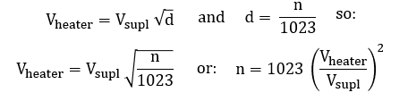
heater voltage
Also the heater voltage is controlled by a 16 bit word of which only the 10 lower bits are used. It is used only in the command string. The word is directly used to program one of the on-chip PWM circuits. The PWM circuit is set at a repetition frequency of 1.2 kHz. When the variable is zero the duty cycle is also zero and the heater voltage is zero. When the variable is 03FFH, the duty cycle is 100% resulting in a heater voltage equal to the supply voltage. There is a quadratic relation between the effective heater voltage and the duty-cycle (d). The relation between the variable (n) and the heater voltage is given by the equations below. Note that to calculate the proper settings for a given heater voltage the actual supply voltage Vsupl is measured as described above.
negative boost converter voltage
The negative boost converter voltage is not a variable which is set by the GUI, but rather it is specified during the initialization of the firmware to a fixed value of -125 V. The relation between the variable (n) and the negative boost converter voltage (Vboost < 0) is given by:
For the uTracerNXT: Vneg = -125 V, R1 = 4.7 kohm and R2 = 240 kohm.
| to top of page | back to uTracer homepage |
Designing and optimizing a circuit like the uTracerNXT is very much a matter of making compromises. It is obviously nearly impossible to satisfy everybodyÆs wishes in one design at a reasonable complexity and cost. On one end of the spectrum, there are people that are interested in characterizing battery tubes at very low voltages and currents, while on the other end of the spectrum people want to test high power tubes at hundreds of volts and milliamps. The uTracer3 with its 400 V and 200 mA anode and current range and -50 V grid bias range proved to be a reasonable compromise for most people. For people who wanted higher currents, there was a relatively simple modification to push the current limit to 600 mA, while for people who needed lower voltages, there was a low voltage option, be it that that required a modified PIC processor.
My original idea for the uTracerNXT was to make it a kind of universal platform so that everybody could tailor the circuit to his (or hers) special needs. However, in discussing the idea with my friend and first hour uTracer user and distinguished tube modeler Derk Reefman, he pointed out that that would make the uTracer much too complicated to be used by the average user. Most users just want to build the circuit, calibrate it without too much fuzz and then use it. His remark set me thinking, and resulted in the compromise discussed in this section, which basically boils down to a ōdefaultö configuration fixed at 500 V @ 250 mA (350 mA see below), and -100 V for the grid bias for the novice user than can be tailored to individual needs by experienced users.
The anode and screen current ranges
LetÆs first start by recapitulating how the current measurement works. The current in either the anode or screen section is measured by measuring the (negative) voltage drop over a current sense resistor Rs. In the case of the anode section in Fig. 7.1 this is resistor R62. This negative voltage drop is then inverted by OpAmp IC60 and fed into the programmable gain amplifier IC61 after which it is measured by the microcontroller. The signal is also directly fed into the microcontroller for the maximum compliance safety feature. This feature immediately switches off the voltages in case a preset current limit is reached. At this point three things must be considered.
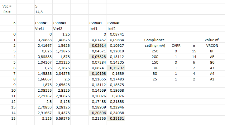
Figure 9.1 The maximum compliance current settings of the uTracerNXT, and how they correspond to the selected reference voltages in the PIC.
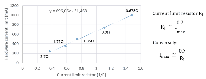
Figure 9.2 Measured hardware current limit value as a function of 1/Rl.
Changing the current ranges, compliance and limits
The current range can be modified by changing the values of the current sense resistors (R62 and R82 in Fig. 7.1). The way this has been organized is that in order to increase the current range, the user can add a resistor (Rca and Rcs) in parallel to the fixed resistor of the default configuration. Similarly additional resistors Rla and Rls can be placed in parallel to the hard current limit resistors R72 and R92. On the PCB space has been reserved for these resistors, and they can be ōactivatedö by placing jumpers (Fig. 9.1). The reason why I have chosen to place resistors in parallel to the original resistors instead of just selecting between two resistors, is that it is then possible that the user forgets to place the jumper all together so that no resistor at all is connected potentially resulting in a dangerous situation. Of course, the GUI needs to know about the changed resistor values, and they need to be calibrated. How this is done is explained at the end of this section. Note that when the anode or screen current range(s) are changed, the GUI needs to be restarted for these changes to take effect. Restarting the GUI will also scale the compliance values with the selected current range (Rs value).
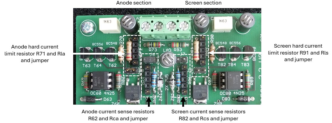
Figure 9.3 Current range and limit modification points on the uTracerNXT
The table in Fig. 9.4 gives a few suggested modifications for several current ranges. The use of the table is best explained by a few examples. In the default configuration the maximum current that can be measured with compliance switched off is 350 mA. When compliance is switched on (recommended for unknown tubes) the maximum current is 250 mA. In the default configuration no additional resistors or jumpers need to be placed.
Now suppose that we want to increase the maximum current range for the anode section to 750 mA. In that case a resistor Rca of 12.4 ohm needs to be connected in parallel to R63, which when the jumper is placed, will result in an equivalent current sense resistor of 14.3//12.4 = 6.64 ohm, resulting in a current range with compliance switched off of 5/6.64 = 750 mA. At the same time a resistor Rla of 1.8 ohm needs to be connected in parallel to R71, which when the jumper is placed will result in an equivalent current limit resistor of 1.8//1.8 = 0.9 ohm, resulting a hard current limit of 0.7/0.9 = 770 mA. With the compliance switched on, the maximum current is 540 mA.
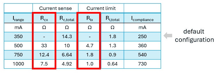
Figure 9.4 Examples of modified current ranges and the resistors that need to be connected in parallel to the current sense and current limit resistors.
In case the anode channel is modified, Rcx and Rlx stand for Rca and Rla respectively.
In case the screen channel is modified, Rcx and Rlx stand for Rcs and Rls respectively.
The anode and screen voltage ranges
Compared to the current range setting, the voltage range setting is relatively straightforward. Since the anode and screen channels are identical, I will use the anode channel as example in this discussion. Looking at the schematic in Fig. 7.1 the anode voltage across C62 is divided down by R64 and R63, and then directly measured by the microcontroller. Compared to the uTracer3, the value of R63 has been increased from 470k to 1M. This is partly because of the higher voltage, but also to reduce the self-heating of the resistor.
Some years ago I published the modifications necessary for the uTracer3 to lower the anode and screen voltage range to below 100 V. To keep sufficient voltage resolution, it is necessary to reduce the voltage divider ratio. Since I recently got several requests for this low voltage option, I thought it made sense to directly include it into the uTracerNXT from the start, rather than to have to publish a modification afterwards.
I decided to implement this option by adding the possibility to lower the value of R63 by connecting resistor Rva in parallel to it by placing jumper J10. Just as with the current range selection, this eliminates the possibility that the user accidentally forgets to connect any resistor at all, in which case the boost converter would keep on charging C62 with disastrous consequences. Although the PCB is already quite full, it was possible to squeeze in the additional components as shown in the design detail shown in Fig. 9.5.
Figure 9.5 Planned modification to the uTracerNXT version 0 PCB to include the low voltage option.
The inclusion of this low voltage option could potentially result in a dangerous situation in case the user removes the jumper to switch back from the low voltage range to the high-voltage range, but forgets to inform the GUI of the modification. In that case a situation could arise whereby the uTracer continues to charge C62 because it cannot reach the setpoint. By increasing R64 to 9.76 k, this dangerous situation is mitigated. In all cases the maximum setpoint value the GUI can communicate to the ADC in the PIC is 1023 (decimal). With R64 = 9.76 k and R63 the maximum possible value of 1 M, even in this case the maximum voltage of C62 is limited to 517 V, which is just slightly above the maximum continuous operating voltage of 500 V and well within the safety margin the manufacturer has built into the capacitors (At Philips e.g. we used to standard test electrolytic capacitors at 120% of their maximum rated voltage).
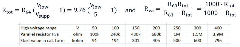
Figure 9.5 Formulas to calculate the parallel resistor Rva for a modified voltage range (see text below), and some pre-calculated examples.
Figure 9.5 shows how, for a given voltage range, the value of resistor Rva parallel to the 1 Mohm resistor R63 is calculated. Note that in these formulas the values of the resistors are all in kohm! First, for a given voltage range the value of the two combined resistors Rtot is calculated. Next, the value of the parallel resistor Rpar is calculated. In the table in Fig. 9.5 the recommended parallel resistor values for a number of voltage ranges is given. So, for example, if the user wants to limit the voltage range to 200 V, a resistor Rva= 680 kohm is recommended, which results in a combined resistance of Rtot = 405 kohm. It is this value (Rtot) which needs to be entered as a starting value for the calibration process in the appropriate field on the calibration form.
Obviously, when the voltage range is changed, also the range of the values the user can enter changes. To not overcomplicate matters, I decided to keep the high-voltage range fixed at 500 V, corresponding to a value of R63 of 1 Mohm. When now the voltage range is decreased, by lowering the value of R63, the new maximum voltage can be calculated from:
During the calibration, the value of R63 is adjusted so that the output voltage corresponds exactly to the set point value. So in the calculation of the low voltage range, this adjusted value for R63 is used.
Finally:
The working and ranging of the grid bias circuit is very simple. A 12-but DAC IC 40 (see Fig. 7.1) generates a voltage between 0 and 5 V. This voltage is then inverted and amplified by OpAmp IC41. The amplification factor is determined by the ratio A = R45/R41. So in the default configuration, the amplification is set to ¢ (200 / 10) = -20. This sets the default grid bias range to 0 to -20 * 5 = -100 V.
The grid bias range can be decreased by lowering the value of R45. Decreasing the grid bias range has the advantage that it increases the resolution at lower voltages. Again here, lowering the value of R45 is done by adding resistor R46 in parallel to R45. In the circuit diagram R46 has been given the value of 68 kohm. When jumper J2 is placed the total feedback resistance is lowered to 200 // 68 = 50.1 kohm, which results in an OpAmp gain of ¢(50 / 10) = 5, so a grid bias range of 0 to -5 * 5 = -25 V.
Although the default grid bias ranges are a good compromise, the user has the possibility to change the grid bias ranges ¢ if so required ¢ by modifying the values of R45 and R46.
Figure 9.6 shows the calibration form of the GUI for the uTracerNXT. The picture shows the situation of the sliders and the entry field after a cold start-up or after the ōReset Calibration Valuesö button has been pressed.
Note that initially the default configuration is:
As indicated in Fig. 9.6, the form contains two different fields and methods to calibrate the uTracerNXT. The top field is primarily meant for novice users who only want to use the standard (see above) configuration. These users are not to touch the fields in the bottom section and only use the sliders. The sliders are linked to the CalVar1-6 variables introduced in the previous section.
Experienced users who want to use the possibility to use the modified ranges (higher currents, lower anode/screen voltages, lower grid voltage) must bring all the sliders to the default position indicated in the figure and calibrate the uTracerNXT by directly editing the values in the entry fields which are directly connected to the resistor values in the different conversion formulas discussed in the previous section. Note that in this way it is possible to define different current and voltage ranges for the anode and screen! So, for instance, it is possible to define a high current and voltage range for the anode, while for the screen lower current and voltage ranges can be used.
Directly editing the resistor values has the additional advantage that in this way no iterative process to find the right values is necessary. By knowing the setpoint, and doing a single measurement, the correct value can be directly calculated. The way this is done will be explained in detail in the manual.
When a value in one of the fields is changed, they take effect immediately. However, when a range is changed it will be necessary to save the calibration file and restart the GUI to update the minimum, maximum and default values of the voltages that can be entered in the main form or in the quick test forms, as well as the compliance values listed in the compliance drop-down selection ōComboBox.ö When a range is changed, the GUI will remind the user to save, close and restart the GUI.
As explained above, the high-voltage range for the anode and screen is fixed to 500 V, implying a resistance value of 1000 kohm. To allow for calibration, this resistance value can be varied between 900 and 1100 kohm to compensate for the component tolerances. When the low voltage range is selected, the user can ¢ if so desired ¢ lower either the anode and/or screen ranges by specifying a different resistor value, e.g. by a value as suggested in Fig. 9.5. Obviously, the values given in Fig. 9.5 are just starting values, that still need to be fine-tuned by calibration. The lowest value that can be entered for the resistance values that can be entered is set to 50 kohm.
As explained above, the default current sense resistor value is 14.3 ohm resulting in a maximum current of 350 mA. To increase the current range of either the anode and/or the screen current channels, a resistor Rcx can be connected in series to the current sense resistor. The table in Fig. 9.4 gives for several current ranges the recommended value of Rcx, and the resultant parallel resistance value of Rcx//14.3 = Rc,total that needs to be entered into the proper field on the calibration form. Obviously, the values given in Fig. 9.4 are just starting values, that still need to be fine-tuned by calibration.
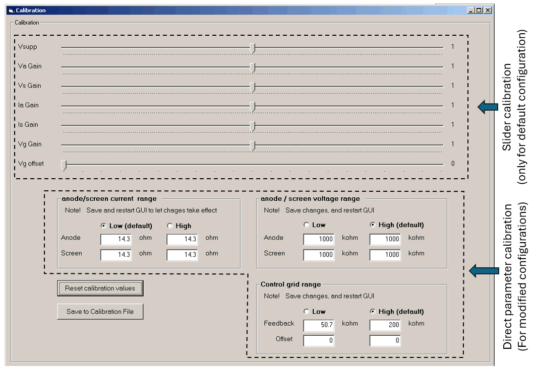
Figure 9.6 The uTracerNXT calibration with default settings and values after ōReset calibration valuesö.
| to top of page | back to uTracer homepage |
One of the most heard ōcomplaintsö about the uTracer3 is its maximum (most negative) grid bias of -50 V. Many, especially high-power tubes have a grid bias working point that is significantly lower. Figure 10.1 shows the Ia(Vg) curve, and the typical bias point for the popular 300B audio output triode. In normal operation the typical grid bias is specified as -60 to -70 V, while for a plate voltage of 450V the cutoff voltage is around -130 V.
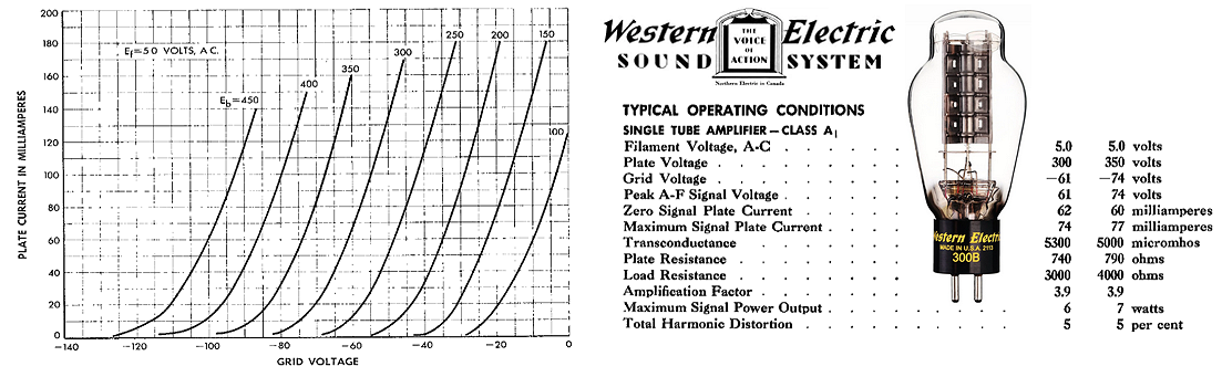
Figure 10.1 300B triode Ia(Vg) curves and typical bias point.
The maximum (most negative) grid bias voltage of the uTracerNXT is determined by the maximum allowed supply voltage of OpAmp IC41. For this OpAmp I selected two candidates, the OPA454 and the OPA455. The OPA454 has a maximum supply voltage (V+ - V-) of 100 V, with an absolute allowable voltage of 120 V. The OPA455 is specified for a maximum operating supply voltage of 150 V, with a maximum allowable voltage of 160 V. My original idea was to go for a maximum grid bias of -100 V using an OPA454, so that I could also substitute an OPA455 in case there are supply issues with the OPA454. However, again lately I received several requests for a grid bias range going down as low as -120 V or preferably even lower. At the writing of this section Mouser has more than 4600 OPA455 on stock, while the stock at Texas Instruments even exceeds 100.000 pieces. By the way, surprisingly they are cheaper when ordered through Mouser than directly at TI! So, since also the price of the OPA454 is only an Euro or so more than the OPA455, there is really no reason why not directly go for the OPA455 and a grid bias range of -140 V.
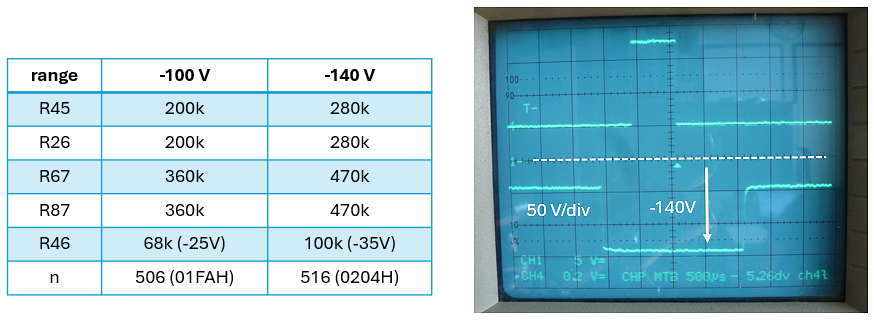
Figure 10.2 Left, component changes needed for the -140 V grid bias range. Right, pulsed grid output test at -140 V, measured with respect to cathode (ground).
For the increased grid bias range, the negative supply voltage of the OPA455 was lowered to -145 V. This combined with the positive supply voltage of +5 V, gives a total supply voltage for the OPA455 of exactly 150 V, still well within the maximum allowable supply voltage of 160 V. Since, according to the OPA455 datasheet, the output swing of the OPA455 is limited to 5 V from the negative supply voltage, this results in a minimum grid bias of -140 V.
The first thing to do is to increase (or decrease if you like) the output voltage of the inverting boost converter to -145 V. This is done by increasing the value of R26 in the feedback voltage divider from 200 K to 280 K. This together with a bit of tweaking of the constant n of the firmware in the PIC, exactly results in a negative supply voltage of -145 V.
As explained in Section 3, OpAmps IC60 and IC80 need a small sink current of approximately 300 uA out of their outputs to pull them down to 0 V. To this end, R67 and R68 are increased to 470k resulting in a sink current of 145 / 470k = 308 uA.
Finally, the gain of the grid circuit OpAmp needs to be set. For the -140 V range, feedback resistor R45 = (140 / Vdac)*R41. With Vdac the maximum output voltage of the DAC at 5 V and R41 = 10 k, we find R45 = 280 k (where have we seen that value before!?). For the smaller grid bias range, I suggest using a 100 k resistor for R46. 100 k in parallel to 280 k gives a combined resistance of 73.7 k, resulting in a grid bias range of (73.7 / 10)*5 = 37 V, or lets round that to -35 V with a bit of overhead.
How about OPA462 ?? In SMD voorraad
| to top of page | back to uTracer homepage |
The standard voltage and current ranges of the uTracerNXT after construction are:
- Anode/Screen voltages 2 ¢ 500 V
- Anode/Screen currents 0 ¢ 350 mA (0 ¢ 250 mA with compliance switched on)
- Control Grid voltage 0 ¢ 120 V
These ranges are a compromise to accommodate the tracing and measurement of a wide variety of tubes. However, sometimes it may be desirable to modify these ranges e.g. to allow higher currents, or to measure battery tubes at low voltages etc. The uTracerNXT has been designed so that it is relatively easy to modify the default ranges, and to switch back and forth between the standard and the personalized configuration.
The measurement ranges are in most cases determined by the value of one or two resistors. This document explains how ranges can be modified by changing resistor values. The way this is done is by adding a resistor in parallel to the ōfixedö default resistor that was installed during the construction of the kit. At first sight this may seem an odd way of changing resistance values! Why not simply switch between two resistors? The reason is that in this way a situation may occur where there is no resistor connected at all! Since this might result in a dangerous situation, we use the ōparallel resistorö method to ensure that there is always a resistor in place.
The uTracerNXT offers two methods for calibration. For the standard configuration the ōslider methodö is used, because many people are familiar with them and it gets you started quickly. However, when the measurement ranges are modified, we must have a means to tell the GUI what changes have been made and also provide a means to calibrate the additional range(s). The way this is done is by directly entering the resistance values that determine the different ranges. In the new procedure the sliders are not used anymore and returned to the starting position (usually ō1ö).
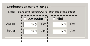
Since the anode and the screen sections of the uTracerNXT are identical and independent, it is possible to select different ranges for the anode and/or screen. In this way it is e.g. possible to define a larger current range for the anode and a smaller current range for the screen.
The figure to the left gives an example of how this is implemented in practice for the current ranges. As can be seen, there are two possible configurations encircled by dashed boxes: the standard ōlow-currentö range, and a ōhigh current range.ö A range is activated by selecting one of the two ōradio buttons.ö Associated with each configuration are an anode and screen current sense resistor. After a reset of the calibration values, all resistor values are initialized to their default value (14.3 ohm). Switching between configurations is done by placing or removing a jumper (or jumpers) and selecting the appropriate range on the calibration form. In most cases the GUI will ask the user to save the configuration form and restart the GUI. This is necessary because the entire GUI needs to be updated for the modified configuration.
In the sections below, the personalization of the ranges of the uTracerNXT is discussed in detail. In these discussions the modification of the anode voltage/current ranges will be used as an example. With the necessary changes the same procedure is used for the screen channel. In all cases, the calibration follows the following steps:
Although this method may seem cumbersome, it really works very well and is faster than the calibration using the sliders. As a starting point it is a good idea to acquaint yourself with the basic functioning of the uTracerNXT hardware so that you get a better feeling of what you are doing.
Index:
The standard grid bias range of the uTracerNXT is 0 to -120 V. The resolution over this range is 29 mV. Although this is already better than the resolution of the uTracer3+, it may be advantageous to make use of the possibility to define a second ¢ smaller ¢ grid bias range to improve the resolution even more.
The grid bias circuit of the uTracerNXT consists of a 12 bit DAC which generates a voltage between 0 and 5 V. Next, an inverting high-voltage OpAmp amplifies the output voltage of the DAC resulting in the desired grid bias. By default, the high-voltage OpAmp uses a 240 kohm feedback resistor. This combined with an input resistor of 10 kohm results in a gain of A = - (240/10) = -24, and thus in a grid voltage range of -24 * 5 = -120V.
The way the grid voltage range is reduced is by adding a resistor in parallel to the 240 kohm feedback resistor. Adding a resistor in parallel eliminates the risk that there accidentally is no feedback resistor connected at all.
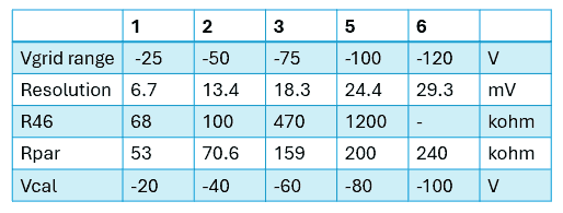
Table 1 Grid bias range ōCookbookö
Although you are free to define your own grid bias range (see Note 1), I have defined some obvious ranges for your convenience (see Table 1). In this table:
In the following the complete procedure to install and calibrate an additional grid bias range will be described. The procedure will be explained using the example of a 0 to -25 V grid bias range (Column 1 in Table 1). If you want to install another grid bias range, you must substitute the respective values for the parameters as indicated in the table. The calibration basically consists of two steps. Since we are not using the sliders anymore, in the first step the 0 to -120 V grid bias range will need to be calibrated again. In the second step, the selected lower grid bias range will be calibrated. Although the whole calibration process perhaps looks a bit intimidating, it is actually quite straight forward. Simply follow the procedure outlined below step-by-step.
It is assumed that you have gone through the basic grid calibration procedure described in the construction manual, and that you know how to measure the grid voltage with a DVM as described in that manual. It is also assumed that, if applicable, you have installed R42 to obtain a positive grid voltage at Vg_set = 0 V.
The description below follows three steps:
preparation
| ▢ | 1 | Ensure that jumpers J2, J3, J4 and J5 are all removed. |
| ▢ | 2 |
Select the desired grid voltage range from Table 1, and lookup the recommended value for R46. Install a resistor with that value on the PCB (location F2). Since in this example a range of -25 V will be installed, a 68 kohm resistor was placed. |
| ▢ | 3 |
Connect a DVM between the grid and cathode connections of your uTracerNXT (See Section 12.2 of the construction manual). |
| ▢ | 4 |
Start the GUI en open the calibration form. Note down the values for the ōVg Gainö and ōVg offsetö sliders so that you can always go back to the old situation. |
| ▢ | 5 | Reset the sliders for ōVg Gainö to 1.0, and ōVg offsetö to 0, and press save to calibration file. |
Calibration of the high-range
| ▢ | 1 | Verify again that jumper J3 is not installed |
| ▢ | 2 |
Verify that the ōHigh (default)ö box is ticked in the ōControl grid rangeö section on the calibration form and that the starting value for the feedback resistances Rg_gain = 240 kohm
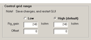
|
| ▢ | 3 | Start a test measurement (see construction manual) with Vgrid set to -100 V, and measure the actual grid voltage Vg_meas. In my case Vg_meas = -101.5 V |
| ▢ | 4 |
Calculate the correction on the feedback resistor from Rnew = Rold*(|Vg_meas/Vg_set|), and enter that value in the appropriate field. In my case Rnew=240*(101.5/100.0) = 243.6 kohm 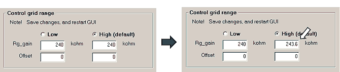
|
| ▢ | 5 | Start a test measurement and verify that the grid voltage is now very close to -100 V |
| ▢ | 6 |
Start a test measurement (see construction manual) with Vgrid set to 0 V. Verify that the measured grid voltage is now slightly positive (between 0 and -100 mV). |
| ▢ | 7 |
Start a test measurement (see construction manual) with Vgrid set to - 0.2 V, and measure the actual measured grid voltage |
| ▢ | 8 |
Increase the value for ōOffsetö (you can only use integer values > 0) Run another test measurement (step 7) and observe the new measured grid voltage. Continue increasing ōOffsetö until the measured voltage is as close as possible to the set voltage (- 0.2 V) Note, that by increasing ōOffsetö you can only make the grid voltage more negative! Note, that the steps you can make are limited by the resolution (see table), in this case 29.3 mV. 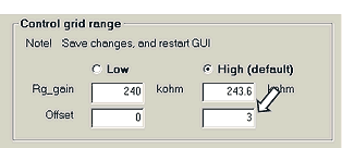
In my case I had to increase ōOffsetö to 3 for the closest match to - 0.2 V |
| ▢ | 9 | Press ōSave to Calibration Fileö |
Calibration of the low-range
| ▢ | 1 |
Install jumper J2 This will connect the 68 kohm resistor that we installed in parallel to the fixed 240 kohm resistor resulting in a nominal combined resistance Rpar = 53 kohm. |
| ▢ | 2 |
Verify that the ōLowö box is ticked in the ōControl grid rangeö section on the calibration form. Read the parallel feedback resistance Rpar from the table and enter that as starting value for Rg_gain in the appropriate field. In this example Rpar = 53 kohm 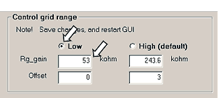
|
| ▢ | 3 |
Read the advised calibration voltage Vcal from the table In this example Vcal = -20 V Start a test measurement (see construction manual) with Vgrid set to Vcal (in this case -20 V), and measure the actual grid voltage Vg_meas. In my case Vg_Meas = -20.2 V |
| ▢ | 4 |
Calculate the correction on the feedback resistor from Rnew = Rold*(|Vg_meas/Vg_set|), and enter that value in the appropriate field. In my case Rnew=53*(20.2/20) = 53.53 kohm 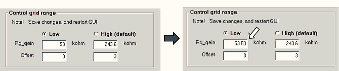
|
| ▢ | 5 | Start a test measurement and verify that the grid voltage is now very close to Vcal, in this example -20 V |
| ▢ | 6 |
Start a test measurement (see construction manual) with Vgrid set to - 0.2 V, and measure the actual measured grid voltage |
| ▢ | 7 |
Increase the value for ōOffsetö (you can only use integer values > 0) Run another test measurement (step 7) and observe the new measured grid voltage. Continue increasing ōOffsetö until the measured voltage is as close as possible to the set voltage (- 0.2 V) Note, that by increasing ōOffsetö you can only make the grid voltage more negative Note, that the steps you can make are limited by the resolution (see table), in this case 6.7 mV. 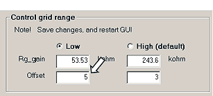
In my case I had to increase ōOffsetö to 5 |
| ▢ | 8 | Press ōSave to Calibration Fileö |
| ▢ | 9 | Do not forget to install jumper J3 to switch on pulsed grid measurements! |
| ▢ | 10 | Do yourself a big favor and note down all the calibration values on a piece of paper as a backup should something with the calibration file! |
Notes
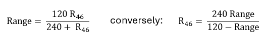
The standard anode and screen current range of the uTracerNXT with the compliance current protection switched off is 0 to 350 mA. With the current compliance protection switched on, the maximum current is 250 mA. Next to the (software) current compliance protection, there is a hardware current protection limit that in the standard configuration is set to 390 mA.
In the uTracerNXT the anode and screen sections are completely separated and identical. This means that the current ranges and limits for the anode and screen sections can be set completely independently. To keep this text readable, I will refer to ōthe currentö instead of the ōanode/screen currentö. Please substitute what is applicable in your case.
The current range and the compliance range are determined by the current sense resistors (R62 for the anode, or R82 for the screen). The current causes a voltage drop over the current sense resistor, which is digitized by a programmable gain amplifier and the ADC of the PIC microcontroller. Since the maximum input voltage of this circuit is 5 V, the maximum current range is: Irange = 5 / Rsense. The hard(ware) current limit is activated when the voltage drop caused by the current over the current limit resistor reaches 0.7 V. So Rlimit = 0.7 / Ilimit. The hard(ware) current limit is set to a somewhat higher value than the maximum current range.
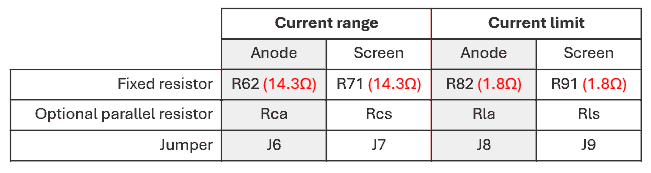
Table 2 Components involved in setting the current ranges and limits.
The components involved in setting the current ranges and limits are listed in Table 2. The default current ranges and limits as they come with the standard kit are determined by the ōfixedö resistors listed in the table. To increase the current range, the respective resistor values need to be lowered. In the uTracerNXT this is done by adding a resistor in parallel to the fixed resistor. This resistor is activated by placing a jumper. Table 2 lists which resistors need to be added and which jumpers need to be placed.
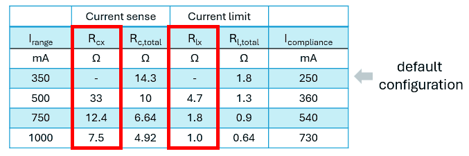
Table 3 Currents range ōCookbookö
Although you are free to define your own current ranges, I defined some obvious ranges in Table 3.
In this table:
In the following the complete procedure is explained to increase the anode current range starting from the standard configuration to 750 mA.
The same procedure, with the necessary changes, applies to current range changes for the screen section.
It is assumed that you have gone through the basic calibration procedure described in the construction manual.
The description below follows three steps:
Preparation
| ▢ | 1 |
Install the pin headers for jumpers J6, J7, J8 and J9. Do not install the jumpers (yet) |
| ▢ | 1 |
Select the desired current range from Table 3, and look up the recommended value for parallel resistors Rcx and Rlx. So, since in this example we want to install a current range of 750 mA for the anode, we insert a resistor of 12.4 ohm for Rca and a resistor of 1.8 ohm for Rla on the indicated positions on the PCB. |
| ▢ | 2 |
Start the GUI en open the calibration form. Note down the values for the ōIa Gainö and ōIs Gainö sliders so that you can always go back to the old situation. |
| ▢ | 3 | Reset the ōIa Gainö and ōIs Gainö sliders to 1.0. From now on we will not be using these sliders anymore but enter the current sense resistance values directly in the bottom section of the form. |
| ▢ | 4 |
Connect a 1 kohm resistor between anode and cathode, and a second 1 kohm resistor between screen and cathode. Preferably these resistors should be 1 Watt and 1%. |
Recalibration of the standard ōLow (default)ö range
| ▢ | 1 | Make sure jumpers J6, J7, J8 and J9 are not installed. |
| ▢ | 2 |
On the main form, switch ōComplianceö to off and make a sweep:
|
| ▢ | 3 |
Plot the anode current and click the cursor on the measured curve somewhere around 300 V. Note down the voltage Vmeas (in V) and the current Imeas (in mA) in this point. 
In my case Vmeas = 277.2 V and Imeas = 278.2 mA. |
| ▢ | 4 |
The correction on the anode current sense resistor is now calculated from
Rnew = Rold * (Imeas / Vmeas), with Imeas in mA and Vmeas in V (see Note 1) So in my case Rnew = 14.3 * (278.2 / 277.2) = 14.35 ohm Einter this value for the low-range anode current sense resistor into the calibration form. 
|
| ▢ | 5 |
Press ōSave to Calibration Fileö Run the measurement again and verify that now: Imeas (in mA) ≅ Vmeas (in V) |
| ▢ | 6 |
Repeat the above procedure but now plot the screen current and modify in the calibration form the low-range screen current resistor. FYI, in my case I had to change the screen resistor to 13.75 ohm. |
Calibration of the new ōHigh-rangeö range
Remember, in this example we install a high-range with and anode current range of 750 mA.
To this end two resistors Rca = 12.4 ohm and Rla = 1.8 ohm were installed.
The screen current range is not modified with respect to the standard configuration.
Make sure the 1 kohm test resistors are still connected to the anode and screen terminals (see preparation section).
| ▢ | 1 | Install jumpers J6 and J7 | ||||||||||||
| ▢ | 2 |
Look up the value for Rc,total in Table 3. This is the combined parallel resistance of the fixed current sense resistor and the additional resistor. For the 750 mA current range example this is 14.3 // 12.4 = 6.64 ohm. Enter this value for the high-range anode current sense resistor into the calibration form. Then select the ōhigh-rangeö, you will now immediately be prompted to save the calibration file and restart the GUI. Do so (see Note 2). 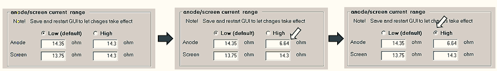
| ||||||||||||
| ▢ | 3 |
Now repeat the procedure exactly as described above! On the main form, switch ōComplianceö to off and make a sweep:
| ||||||||||||
| ▢ | 4 |
Plot the anode current and click the cursor on the measured curve somewhere around 300 V. Note down the voltage Vmeas (in V) and the current Imeas (in mA) in this point. 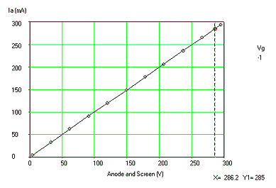
In my case Vmeas = 286.2 V and Imeas = 285 mA. ▢ | 5 |
The correction on the anode current sense resistor is now calculated from
Rnew = Rold * (Imeas / Vmeas), with Imeas in mA and Vmeas in V | So in my case Rnew = 6.64 * (285 / 286.2) = 6.61 ohm Enter this value for the low-range anode current sense resistor into the calibration form. 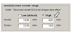
▢ | 6 |
Press ōSave to Calibration Fileö | Run the measurement again and verify that now: Imeas (in mA) ≅ Vmeas (in V) ▢ | 7 |
In this example we did not change the screen current range, so we can simply copy the value for the ōlow currentö range to the ōhigh currentö range.
| 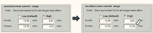
Press ōSave to Calibration Fileö to save the configuration. ▢ | 8 |
Do yourself a big favor and note down all the calibration values on a piece of paper as a backup should something with the calibration file!
| |
Notes:

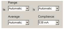
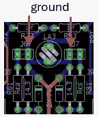
As mentioned before, the current range of the uTracerNXT is a compromise to allow for the characterization of a wide range of tubes as possible. The previous section described how the current range can be extended towards higher currents. In this section we will discuss the extension of the current range towards lower currents. This may be useful for the characterization of e.g. battery tubes.
Before discussing how the current range can be shifted towards lower currents, I recommend that you first familiarize yourself with the previous section ōHigher Anode/Screen Currents.ö In the standard configuration, the uTracerNXT can accurately trace/measure currents starting from approximately 0.5 mA. For even lower currents the measurements tend to become a bit noisy as the voltage drop over the current sense resistor (14.3 ohm) becomes very small. To shift the current range towards lower currents it is necessary to increase the current sense resistor value. Since the input voltage of the ADC on the PIC is given by V = I * Rsense and the maximum V is 5 V, this implies that the current range on the high side will be reduced.
Extending the current range to lower currents implies that the fixed current resistors R62 and/or R82 need to be replaced with a resistor with a higher value!
In this section, by way of example, we will describe how you can modify your uTracerNXT to create two current ranges for both the anode as well as the screen sections. A low-range from 0 to 50 mA, and a high-range from 0 to 320 mA. For both ranges, I suggest using the default current limit resistor of 1.8 ohm setting the current limit for both ranges to 390 mA.
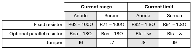
Table 4 Suggested modifications for a low-range of 50 mA and a high-range of 320 mA
Table 4 suggests the modifications necessary for the realization of a 50 mA and 390 mA range. For the low-range a 100 ohm current sense resistor is used. Note that at 50 mA this exactly results in a voltage drop of 0.05 * 100 = 5 V, the maximum input voltage of the ADC. When the jumper is placed, a resistor of 18 ohm is connected in parallel to the 100 ohm fixed resistor, resulting in a combined resistance of 100 // 18 = 15.3 ohm. This results in a current range of 5 / 15.3 = 326 mA, rounded to 320 mA.
The description below follows three steps:
Preparation
| ▢ | 1 |
Install the pin headers for jumpers J6, J7, J8 and J9. Do not install the jumpers (yet) |
| ▢ | 1 | Remove the 14.3 ohm resistors R62 and R82 that come with the standard kit configuration and replace them with 100 ohm resistors. |
| ▢ | 2 | Install two 18 ohm resistors for Rca and Rcs |
| ▢ | 3 |
Start the GUI en open the calibration form. Note down the values for the ōIa Gainö and ōIs Gainö sliders so that you can always go back to the old situation. |
| ▢ | 4 | Reset the ōIa Gainö and ōIs Gainö sliders to 1.0. From now on we will not be using these sliders anymore but directly enter the current sense resistance values into the bottom section of the form. |
| ▢ | 5 |
Make sure that you have selected the ōlow-rangeö and enter the values below into the respective fields. Note that 15.3 ohm is of course the parallel combination of 100 ohm and 18 ohm. 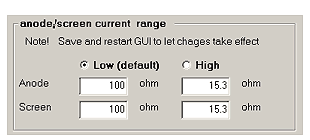 Press ōSave to Calibration Fileö |
Calibration of the 50 mA low-range
| ▢ | 1 |
Connect a 10 kohm resistor between anode and cathode, and a second 10 kohm resistor between screen and cathode. Preferably these resistors should be 1%. |
| ▢ | 2 | Make sure jumpers J6, J7, J8 and J9 are not installed. |
| ▢ | 3 |
Make a voltage sweep: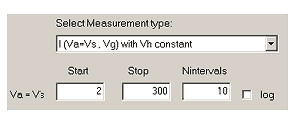
|
| ▢ | 4 |
Plot the anode current and click the cursor on the measured curve somewhere around 300 V. Note down the voltage Vmeas (in V) and the current Imeas (in mA) in this point. 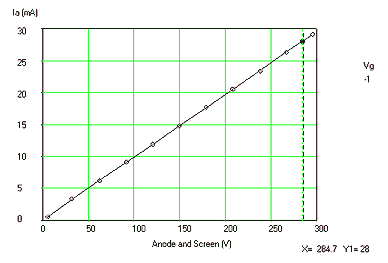
In my case Vmeas = 284.7 V and Imeas = 28 mA. |
| ▢ | 5 |
The correction on the anode current sense resistor is now calculated from: Rnew = Rold * (Rmeas* Imeas / Vmeas), with Rmeas in kohm, Imeas in mA and Vmeas in V (see Note 1) So in my case Rnew = 100 * (10 * 28 / 284.7) = 98.34 ohm Enter this value for the low-range anode current sense resistor into the calibration form. 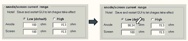
|
| ▢ | 6 |
Press ōSave to Calibration Fileö Run the measurement again and verify that now: 10 * Imeas (in mA) ≅ Vmeas (in V) |
| ▢ | 7 |
Repeat the above procedure but now plot the screen current and modify on the calibration form the low-range screen current resistor. FYI, in my case I had to change the screen resistor to 98 ohm. 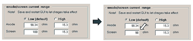
|
Calibration of the 320 mA high-range
| ▢ | 1 |
Connect a 1 kohm resistor between anode and cathode, and a second 1 kohm resistor between screen and cathode. Preferably these resistors should be 1%. | ||||||||||||
| ▢ | 2 | Install jumpers J6 and J7 | ||||||||||||
| ▢ | 3 |
Select the ōhigh-range.ö You will now immediately be prompted to save the calibration file and restart the GUI. Do so (see Note 2). 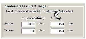
| ||||||||||||
| ▢ | 4 |
On the main form, switch ōComplianceö to off and make a sweep:
| ||||||||||||
| ▢ | 5 |
Plot the anode current and click the cursor on the measured curve somewhere around 300 V. Note down the voltage Vmeas (in V) and the current Imeas (in mA) in this point. 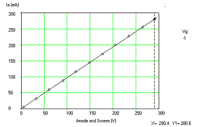
In my case Vmeas = 290.4 V and Imeas = 280.6 mA. ▢ | 6 |
The correction on the anode current sense resistor is now calculated from: | Rnew = Rold * (Rmeas* Imeas / Vmeas), with Rmeas in kohm, Imeas in mA and Vmeas in V (see Note 1) So in my case Rnew = 15.3 * (1 * 280.6 / 290.4) = 14.8 ohm Enter this value for the low-range anode current sense resistor into the calibration form. 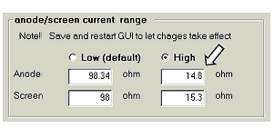
▢ | 7 |
Press ōSave to Calibration Fileö | Run the measurement again and verify that now Imeas (in mA) ≅ Vmeas (in V) ▢ | 8 |
Repeat the above procedure but now plot the screen current and modify in the calibration form the low-range screen current resistor. | FYI, in my case I had to change the screen resistor to 15.1 ohm. 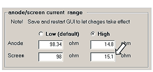 Press ōSave to Calibration Fileö ▢ | 9 |
Do yourself a big favor and note down all the calibration values on a piece of paper as a backup should something with the calibration file!
| |
Notes:
To keep this text readable, I will refer to ōvoltageö instead of the ōanode/screen voltageö. Please substitute what is applicable in your case. The standard voltage range of the uTracerNXT is 2 to 500 V. Since the ADC of the PIC microcontroller has a 10 bit resolution, this implies that the voltage resolution is 500 / 1024 ≅ 0.5 V. For most measurements this is more than good enough, however, if you are tracing / testing low voltage tubes, it might be advantageous to reduce the voltage range and thus increase the voltage resolution. This especially holds for battery tubes with an operating voltage below 100 V. When you use the standard configuration of the uTracerNXT this will result in rather ōnoisyö measurements. By reducing the voltage range, you will obtain perfect curves.
In the uTracerNXT the anode and screen sections are completely separated and identical. This implies that the ranges of the anode and screen sections can be set completely independent. In this section the procedure is explained to lower the anode voltage range. The modification of the screen voltage range is performed - mutatis mutandis - exactly the same way.
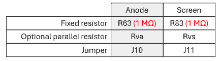
Table 5 Components involved in setting the anode and screen voltage ranges.
The PIC microcontroller monitors the voltage of the 100 uF / 500 V reservoir capacitors by means of a 1000:1 voltage divider which reduces the maximum voltage of 500 V to 5 V. This voltage divider consists of a fixed 9.76 kohm resistor on the low-side and a 1000 Mohm resistor on the high-side. The voltage range is reduced by adding a resistor parallel to the 1 Mohm resistor. This parallel resistor is activated by a jumper. The components involved in the setting of the voltages are listed in Table 5.
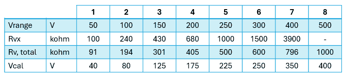
Table 6 Voltage range ōCookbookö
Although you are free to define your own voltage ranges, I defined a few obvious ranges in Table 6.
In this table:
It is assumed that you have gone through the basic boost converter calibration procedure described in the construction manual (Section 12.3), and that you know how to measure the anode/screen voltages with a DVM as described in that manual.
In this example we will define and calibrate a 2 ¢ 100 V ōlow-rangeö for the anode. Modifying the screen range works exactly the same.
The description below follows three steps:
preparation
| ▢ | 1 |
Install the pin headers for jumpers J10 and J11. Do not install the jumpers (yet) |
| ▢ | 2 |
Select the desired voltage range from Table 6, and lookup the recommended value for Rvx. Install a resistor with that value on the PCB (location A4). Since in this example a range of -100 V is selected, a 240 kohm resistor was installed. |
| ▢ | 3 |
Connect a DVM between the + of the 100 uF / 500 V anode capacitor (C62) and cathode connection of your uTracerNXT (See Section 12.3 of the construction manual). |
| ▢ | 4 |
Start the GUI en open the calibration form. Note down the values for the ōVa Gainö and ōVs Gainö sliders so that you can always go back to the old situation. |
| ▢ | 5 | Reset the sliders for ōVa Gainö to 1.0, and ōVs Gainö to 1.0 and press save to calibration file. |
Recalibration of the standard 500 V range
| ▢ | 1 |
Verify that your DVM is still connected to the + of C62 and the cathode terminal of the uTracer, and perform the measurement of the anode voltage with Va=Vs set to 400 V exactly as described in the construction manual Section 12.3. Note down the measured anode voltage: Vmeas. In my case Vmeas = 403 V |
| ▢ | 2 |
The correction of the high-range anode resistor is now calculated from
Rnew = Rold * (Vmeas / Vset). So in my case Rnew = 1000 * (403 / 400) = 1007.5 kohm Enter this value for the high-range anode resistor: 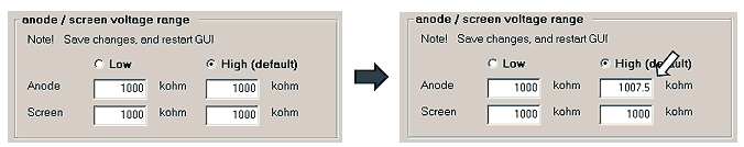
|
| ▢ | 3 |
Press ōSave to Calibration Fileö Perform a second measurement and verify that now Vanode ≅ 400 V. |
| ▢ | 4 |
Now connect your DVM between the + of the screen 100 uF / 500 V capacitor C82 and the cathode terminal of the uTracer, and perform the same measurement. Note down the measured anode voltage: Vmeas. In my case Vmeas = 404 V |
| ▢ | 5 |
The correction on the high-range screen resistor is now calculated from
Rnew = Rold * (Vmeas / Vset). So in my case Rnew = 1000 * (404 / 400) = 1010 kohm Fill in this value for the high-range screen resistor: 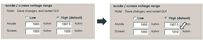
|
| ▢ | 6 |
Press ōSave to Calibration Fileö Perform a second measurement and verify that now Vscreen ≅ 400 V. |
Calibration of new 100 V anode low-range.
| ▢ | 1 | Connect your DVM again between the + of the anode 100 uF / 500 V capacitor C62 and the cathode terminal of the uTracer |
| ▢ | 2 |
Place jumper J10. This connects the 240 kohm resistor Rva parallel to the fixed 1 Mohm resistor, resulting in a combined resistance Rv,total = 194 kohm |
| ▢ | 3 |
Fill in the value of Rv,total = 194 kohm in the proper low-range field on the calibration form, and select the low-range. You will now be prompted to save the calibration file and restart the GUI. Do so (see Note 1). 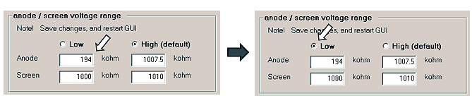
|
| ▢ | 4 |
Perform the calibration measurement as described above and in Section 12.3 of the construction manual, but now with Va=Vs set to 80 V, which is the value Vcal suggested in Table 6. Note down the measured anode voltage Vmeas. In my case Vmeas = 80.2 V |
| ▢ | 5 |
The correction on the low-range anode resistor is now calculated from
Rnew = Rold * (Vmeas / Vset). So in my case Rnew = 194 * (80.2 / 80) = 194.5 kohm Enter this value for the low-range anode resistor: 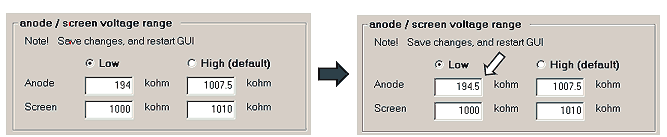
|
| ▢ | 6 |
Press ōSave to Calibration Fileö Perform a second measurement and verify that now Vanode ≅ 80 V. |
| ▢ | 7 |
In this example we did not change the screen voltage range, so we can simply copy the value for the ōhigh-voltageö range to the ōlow-voltageö range.
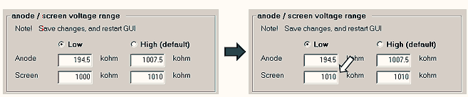
Press ōSave to Calibration Fileö to save the configuration. |
| ▢ | 8 | Do yourself a big favor and note down all the calibration values on a piece of paper as a backup should something with the calibration file! |
Notes:
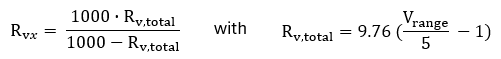
Most of you will know Ihor Smal from the very nice and modern uTracer user interface uTracerJS. This GUI is written in Java Script and runs from your internet browser and is therefore fully Operating System independent. Recently, Ihor extended uTracerJS so that it now also interfaces with the uTracerNXT. Please visit his website for more information and to download uTracerJS: https://boffin.nl/wp/.
Ihor also made a brilliant enclosure for the uTracerNXT that I donÆt want to withhold you. Very cleverly he mounted the LEDÆs and the jumper headers on the backside of the PCB, and 3D printed an enclosure so that the jumper headers are conveniently accessible! I think the photographs below explain the idea better than I could do with words. Ihor was so kind to share his design on MakerWorld.
(https://makerworld.com/en/models/2805915-utracernxt-case#profileId-3125069). On the same page you will also find references to the components (DVMs, heater supply etc.) Ihor used and links to where they can be sourced.
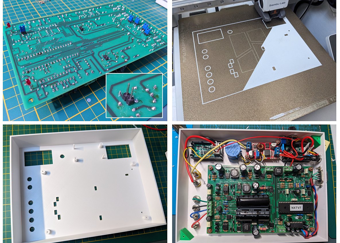
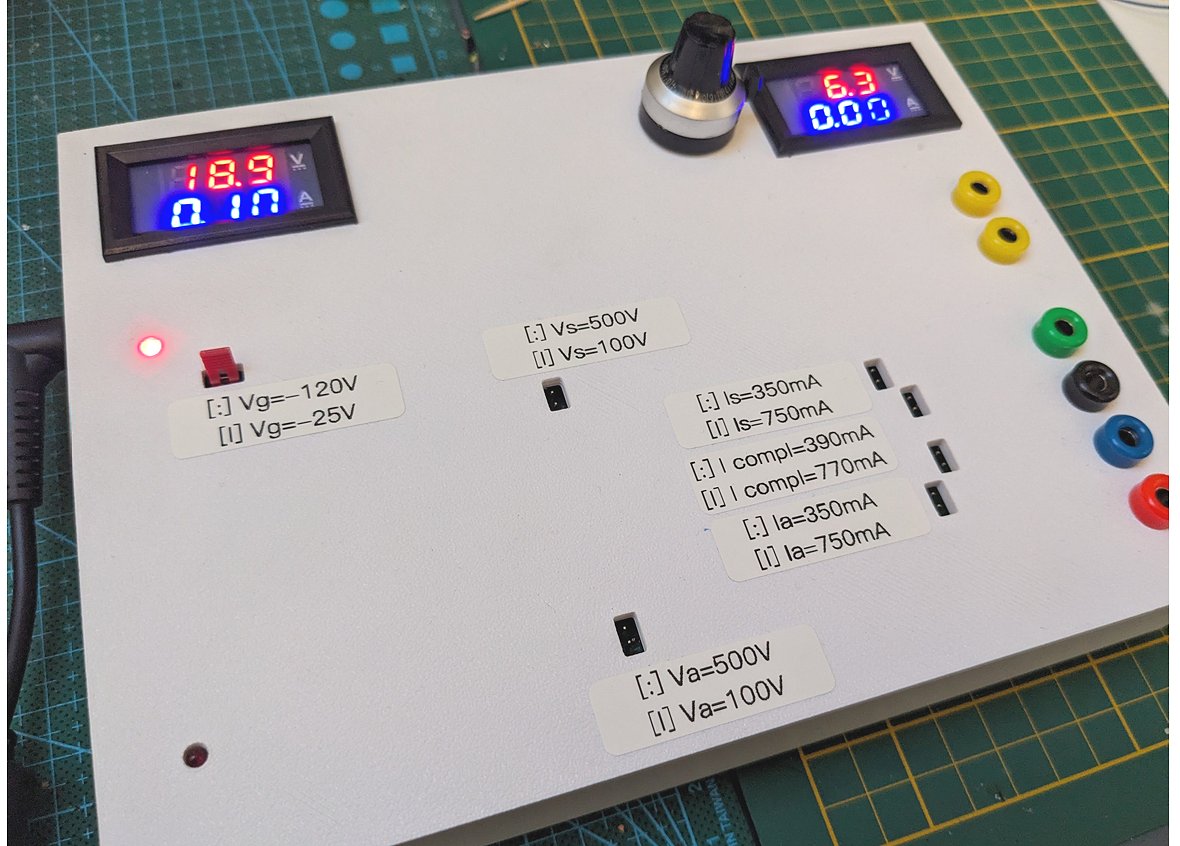
| to top of page | back to uTracer homepage |