 |
 |
 |
|
|
|
I think that I am not exaggerating when I write that the uTracer3+ has been an unexpected and enormous success. At the moment of writing these lines in excess of 1550 uTracer3+ are in service in 55 countries! The uTracer3+ is a compromise between simplicity and performance and was originally intended for my private use only. It was designed to trace and test the majority of the tubes that are being used in amplifiers, radios and televisions. Nevertheless, over the years people have continuously asked me for a tester/tracer with extended capabilities, especially towards higher voltages.
Sense and Simplicity
Personally I rather doubt the need for testing/tracing at higher anode and screen voltages. It is true that in some audio amplifiers supply voltages as high as 800 V are used, but I think that most of the interesting tube parameters can be well characterized at voltages between 0 and 400 V, while for higher voltages the curves can simply be extrapolated. Nevertheless, I agree that especially for RF transmitter tubes higher voltages would be welcome. With higher voltages comes ôin one breathö the wish for higher currents. A uTracer for higher voltages and currents doesnĺt make much sense if not also the grid bias range is being revised, and not only to more negative values, but for transmitter tubes also to positive grid biases. With positive grid biases also comes the need to measure the grid current ů..
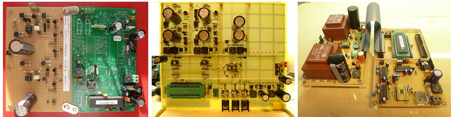
Figure 1.1 Studies for a new uTracer that on their way ended up in ôthe valley-of-death.ö Left, prototype for the high voltage supply/switch of the uTracer5 (never published).
Center, perfboard version of the uTracer5. Right, prototype for the high voltage supply/switch of the uTracer4.
When one starts thinking about the requirements for a next generation uTracer, before you know it you end up with a monster that is designed to do everything, but that has lost all the ôSense and Simplicityö of the original uTracer3. This problem has been hampering me over the past years in developing a new uTracer. Figure 1.1 shows some of the attempts for a new uTracer that I have been working on during the past years. Some of these attempts were published, such as the uTracer4, while other attempts never reached my webpages. Most of these attempts failed because the design became unmanageable complex losing all the charm of the original uTracer. Hoping to have learned from all these failed attempts, I decided to have a new go at a uTracer that offers improved performance, but still has the simplicity and elegance of the uTracer3.
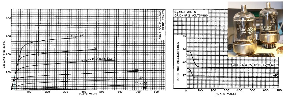
Figure 1.2 The 6146B is a popular tube amongst radio amateurs. I made it the ôtarget tubeö for the uTracer6.
Sometime ago somebody gave me a couple of 6146B beam power tubes. Searching the internet I discovered that the 6146B is a very popular transmitting tube used by radio amateurs. On studying the 6146B data sheet I found that this is the kind of tube that would really need all the new features I have in mind for a possible uTracer6! Voltages up to 800 V, currents in excess of 500 mA, and both positive and negative grid biases. So I decided to take the set of curves of Fig. 1.2 as a kind of target for the uTracer6 specifications.
Based on the experience with the uTracer3, the never finished concepts for the uTracer4 and 5, as well as the experiments published in the Lab Notebook page, I think I have a feeling of what is reasonably possible, and from this I come to the following tentative uTracer6 specifications:
In the following pages we will investigate how realistic these specifications are. One thing that I have learned the past years is to make incremental steps. So both for the hardware, but especially also for the software I will stay as closely as possible with what is there for the uTracer3. As usual I will include some ôpersonal memorabiliaö in these pages, mainly for myself since these pages primarily serve as my own documentation and I like to be remembered of happy personal events that happened concurrent to the experiments/writing of this work.
| to top of page | back to uTracer homepage |
Increasing the anode and screen voltages of the uTracer is not so easy. First of all, because the maximum working voltage of electrolytic capacitors is fundamentally limited to around 450 V. Secondly, boost converters are not really ideal for generating very high voltages. This is because the maximum voltage that can be applied over an inductor is limited, but more importantly, boostconverters require a switching transistor that has both a very low on-resistance as well as a very high working voltage, which are conflicting requirements.
More suitable are flyback converters. Flyback converters use a transformer to generate the high voltage. A very nice property of the flyback converter is that the switching transistor on the primary side ôdoes not seeö the high voltage on the secondary side, but only a voltage that is scaled down according to transformation ratio of the transformer. This makes the selection of the switching transistor much easier since on-resistance and output voltage now basically have been decoupled. If you want to know more about the basics of flyback converters have a look at a page that I wrote ages ago.
Unfortunately, flyback converters have one, for hobbyists, huge drawback: they require a transformer. Among hobbyists, including myself, transformers are not very popular. Either you have to make them yourself (ů) or you have to rely on what is commercially available, which is usually not that much. However, some time ago I uncovered a cute little transformer that at first side might be perfectly suitable for experimenting with higher voltages for the uTracer. The transformer in question is manufactured by WŘrth with type number 750311486, and is available from Mouser with type number 710-750311692.
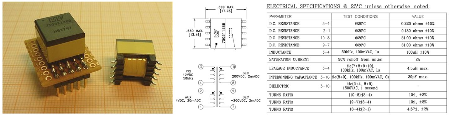
Figure 2.1 The 750311486 flyback transformer from WŘrth.
This little gem, which measures something less than a cube centimetre has four windings. A primary winding with an inductance of 80 uH, and two secondary windings, each with 10 times more windings than the primary winding. My idea was to use both secondary windings in series to generate voltages towards 1000 V. Figure 2.2 shows a simple first test circuit to see if a flyback converter around this transformer would fit into the uTracer concept. The circuit consists of an oscillator that generates 10us wide pulses at a repetition frequency of 10 kHz. On the secondary side, the two secondary windings feed two 100 uF / 450 V capacitors in series. A tricky pitfall of this circuit is the isolation between the two secondary windings. According to the specifications, the isolation between the primary and secondary windings is specified at 1500 V. However, this is the isolation between primary side and secondary side. It says nothing about the isolation between the two secondary windings. To make it for the transformer as easy as possible, I made an elaborate construction with D1 ů D4 that ensures there is no DC potential between the two secondary windings. Only during the flyback phase, there is a very short moment when all diodes are conducting, and where there can be up to 900 V between the two windings.
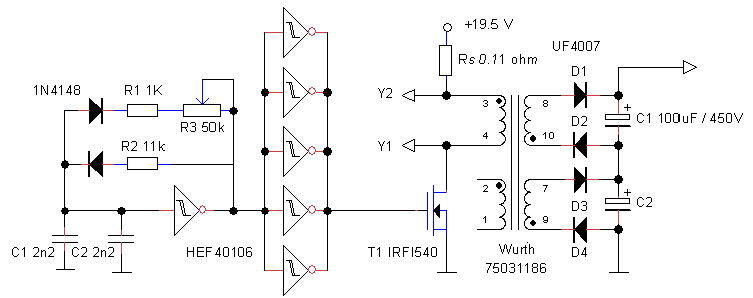
Figure 2.2 Circuit used to test the 750311486 flyback transformer from WŘrth under conditions resembling the uTracer topology.
The circuit worked like a dream. In less than six seconds, the circuit charged the capacitors to 900 V! There was no sign of dielectric breakdown between the secondary windings. Note that at the primary side a simple IRFI540 transistor was used that is specified at 77 mOhm on resistance with a breakdown voltage of only 100 V.
Figure 2.3 Full blown test circuit that I use(d) to study circuit concepts to increase the working voltage of the uTracer.
On the perfboard there is a second ôpiggybackö perfboard that allows me to test different inductor/transformer configurations.
The next step was to try the flyback transformer in an actual uTracer setup. Figure 2.3 shows a hacked uTracer where the high voltage section has been replaced by a breadboard flyback implementation. The breadboard contains the high voltage section in a flexible and reconfigurable configuration, and a new high voltage switch (more about that in a future write-up). Because I donĺt want to completely change the uTracerĺs firmware, the flyback converter is driven in the same way as the standard uTracer, so with pulses of a variable length (0 to 50 us) with a repetition frequency of 10 kHz. The uTracer measures the voltage and stops pulsing when the voltage reaches the set point value. To my surprize and disappointment the circuit worked less well than I expected. The curves were raged, especially for voltages below 150 V. Considerable time was spent on debugging the circuit. At first I suspected the oscillations that are common to flyback converters and that are caused by the charge stored on the drain of the MOSFET that cause oscillations after the transformer has delivered its charge to the load capacitor. Adding snubbers and diodes did give some improvement, but the circuit still continued to perform unsatisfactory.
I sometimes have the bad habit to start experimenting straight away without thinking too much or making calculations/simulations first. I plead guilty! After the initial disappointment I made some basic calculations that gave some clues as to why things didnĺt work as expected. The most basic equation for any boost or flyback converter is given in Fig. 2.4A. It gives the current in an inductor with inductance L when it is applied to a voltage source Vsupl for t seconds. It basically says, when an inductance is connected to a voltage source, the current through the inductor increases linearly with time and at a rate inversely proportional to the inductance. Letĺs take the flyback transformer as an example (Fig. 2.4B). If we apply 20 V during 15 us to the 100 uH primary winding, the current in the primary winding will rise to 2 A, the maximum current before the core starts to saturate.
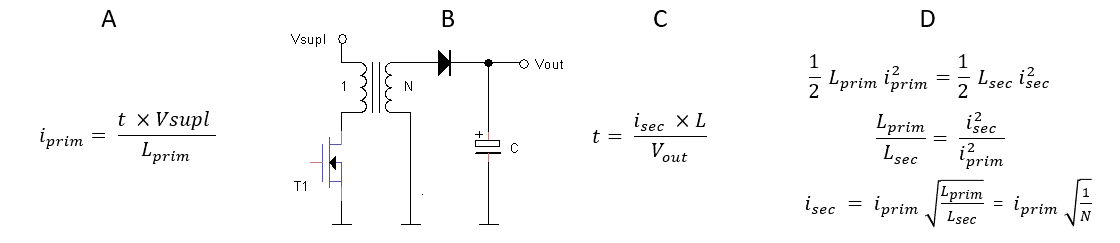
Figure 2.4 Basic equation(s) governing working of a flyback converter.
When T1 is opened, the magnetic energy stored in the transformer will be dumped in the capacitor. The initial current flowing in the secondary side simply follows from the fact that the energy initially stored on the primary side of the transformer, is now transferred to the secondary side (Fig. 2.4D). So with a ratio in turns of a factor 10, the initial current on the secondary side is 2*sqrt(0.1)= 0.63 A. Here we see one of the reasons why the circuit is not working as expected. The secondary current causes a large voltage drop over the secondary winding amounting to 0.63*62= 39 V! This not only interferes with the proper flyback operation at low output voltages, but it also gives rise to substantial dissipation as could also be felt by the temperature of the transformer.
Back to the good old boost converter
After a lot of playing and tweaking of the flyback circuit, some improvement in the performance of the circuit was obtained, but it was too much of a hassle; the elegance of the circuit was lost.
Playing with the flyback converter, I realized however, that in the boost converter concept the problem of a too high voltage over a single inductor could be solved by using two inductors in series! From the uTracer3 we know that this type of inductors can easily handle 450 V across their terminals. By placing two inductors with half the inductance value in series, the current will flow through both inductors and consequently the generated voltage, which is proportional to dI/dt, will by definition be equally divided over the two inductors, potentially boosting the voltage up to 900 V
Anode and screen voltages up to 900 V would be great of course, but the problem of a switching transistor that can handle 1000 V with a sufficiently low on-resistance and acceptable price and availability remained a problem. Fortunately it appeared that since the uTracer3 the industry has made significant progress. Silicon Carbide transistors with incredible specifications have now become available at very acceptable prices. An example is the SCT2750NY from ROHM that is available from Mouser under part number
755-SCT2750NYTB. This 1x1cm ômonsterö has a breakdown voltage of 1700 V, and an on-resistance of only 0.75 Ohm. It can handle currents up to 6 A, a power dissipation of 57 W, and comes at a price of around 6 euros. Apart from its large TO-268-2L package, the only other drawback that I can think of is that for the device to handle substantial currents, a gate voltage of around 15 V is required.
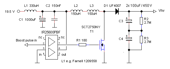
Figure 2.5 900 V Boost converter module.
Figure 2.5 shows the basic circuit of the high voltage boost converter. The circuit is pretty straightforward. The gate of the SiC fet is driven by a dual gate driver circuit. I used an IR25600, but many other gate driver ICs (like the MIC4427) will do just as well. The 8 pin package contains two driver circuits so that one can be used for the anode section and the other for the screen section. Resistor R1 limits the gate current during switching to a safe value. The filter consisting of L1 and C1 smooths out the high current boost pulses, which helps to reduce noise in the system. Finally, the two 2.7 M resistors R2 and R3 ensure that the output voltage is equally divided over C3 and C4 even when is a small difference in leakage current in these capacitors.
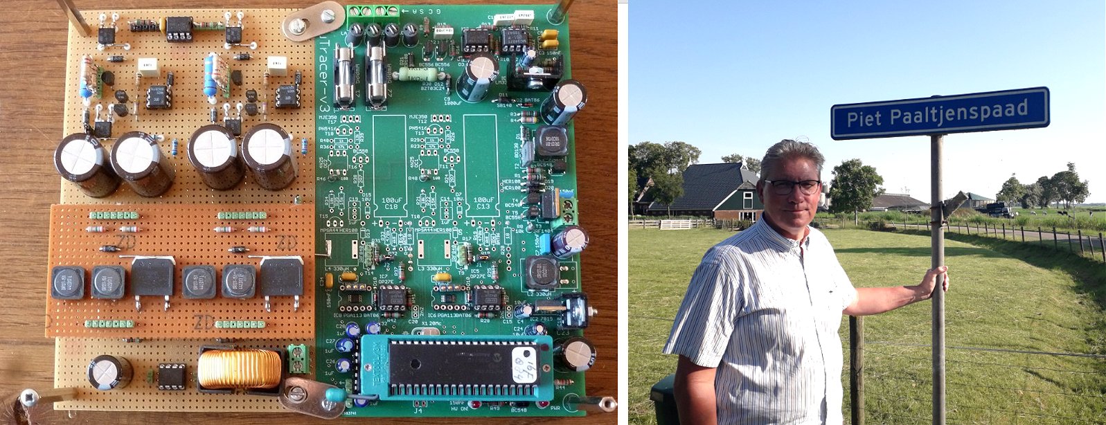
Figure 2.6 To the left the modular test uTracer now with the boost converter installed. Note the large size of the SiC transistor! The picture on the right is just a small souvenir for myself of the holiday spent in Friensland in the North of Holland where we visited Foudgum, a tiny village in the North of Holland where the Dutch writer and poet Piet Paaltjens lived (summer 2019).
Figure 2.6 shows the same test board as in Fig. 2.3, but now equipped with the boost converter. The circuit worked like a dream, without any hitches! Note the enormous size of the SiC SCT2750 in comparison to the inductors! An added benefit of the circuit is that the saturation current of the 150 uH inductors is much higher than the 330 uH inductors in the uTracer3: 3 A vs 1.5 A. By simply increasing the length of the boost converter pulses to 35 us, this current is reached. Since the energy stored in an inductor is proportional to the current squared, this means that per boost converter cycle 4 times the amount of energy (charge) is transferred to the capacitor(s). In plain English, they charge much faster, especially for voltages in the lower range.
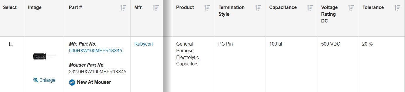
Figure 2.7 The new 100 uF / 500 V capacitors from Rubicon (datasheet).
I had just finished writing this article when I found that Rubycon is now offering 100 uF capacitors at a working voltage of 500 V! There are more 100 uF / 500 V capacitors available, but they are of the bulkier snap-in type. The new Rubycon capacitors have the same diameter (18 mm) and pin spacing (7.5 mm) as the capacitors used in the uTracer. Using 2 of these capacitors in series would in principle make a 1000 V uTracer possible! Unfortunately these capacitors have a very long lead time of 20 weeks (!!) and Mouser does not have then on stock. Still, I ordered a bunch of them, and they will be delivered in April.
After I published this section, Georg Grossmann sent me a few considerations that I find valuable enough to reproduce below:
A uTracer for 1000V and 1000 mA ( and +/- 100V grid!) is a formidable goal. I'm looking forward to see your approach to solve the numerous challenges ahead.
Studying your elaboration on HV generation, a few concerns have come to my mind. As you have stated yourself, the classical boot converter seems to have come to its limits. Using a flyback transformer looks much more elegant. When I tried to understand why you couldn't get it to work well enough, a few learnings from own (unsuccessful) experiences came to my mind.
The current in the primary coil should stay safely below saturation. In your example, (100 uH, 20V) you have an initial rise in current of 200mA/us. Since effective inductivity falls with higher currents, this rate increases a lot nearing saturation. That implies that saturation is probably reached earlier than assumed in your example, leading to much higher peak currents than intended in the primary coil.
I'm not so sure about your assumption regarding the voltage loss in the secondary windings. The benefit of the transformer is of course that it increases the voltage by the ratio of secondary to primary windings. Currents are decreased by the inverse of this ratio. The last line of Formula 2.4 D is suggesting that the inductivities of transformer coils are proportional to the number of windings, which is not correct. A simple approach gives a secondary peak current in both secondary coils of Ipr/20, about 100mA at saturation and 3.1 V loss in each coil.
A possible cause for the unstable behaviour of the flyback design at lower voltages could be that the design requires the magnetic flux in the transformer to be zero before each new pulse. Otherwise the current in the primary coil will not start at zero, leading to an even earlier saturation and unwanted dramatic increase of current. At lower voltages, the time needed for the secondary current to fall to 0 can be longer than the 100us given by the 10kHz pulse frequency. The combined inductivity of both coils in series should be about 40 mH. To fall from 100mA to zero in less than 100us a voltage of at least 40V is needed.
Maybe the flyback design deserves a second try. Adapting both the primary switch-on time and the pulse frequency to avoid saturation could do the trick. That would allow the use of standard MOSFETs directly driven by the MCU and promises also a higher conversion efficiency.
I hope to see more of your very interesting experiments and design concepts soon.
Generating the required high voltages is of course only one part of the story of a higher voltage uTracer. We also need a high voltage switch that can handle 900V, or with a safety margin 1000V, and that can operate in a floating mode. The uTracer3 uses a simple PNP switch. As it turns out, it is very difficult to find affordable PNP or PMOS devices for such high voltages. However, NPN and NMOS devices for these voltages are readily available. In general N-type devices require a more complex driver circuit because the gate voltage has to be controlled with respect to the source that is floating. The gate voltage even has to become higher than the high side voltage rail when the device is fully on! As it turns out, for this application, also the P-type solution would require a special driver scheme to galvanically isolate the high voltage switch from the rest of the circuit, so in complexity there is not much difference. Having decided for an N-type device we still have to make the choice between an NPN bipolar transistor or an N-Channel MOSFET. Given the fact that for the MOSFET we donĺt have to bother with a static gate current and that suitable high-voltage NMOS transistors are relatively cheap, the choice was easy. At first sight suitable transistors are the FQD2N100 from Fairchild or the STD2NK100Z from ST Microelectronics. These transistors have an on resistance of resp. 9 and 6 ohm, more or less independent of the drain current, so that it is quite straightforward to compensate for the voltage drop over the transistor after the measurement.
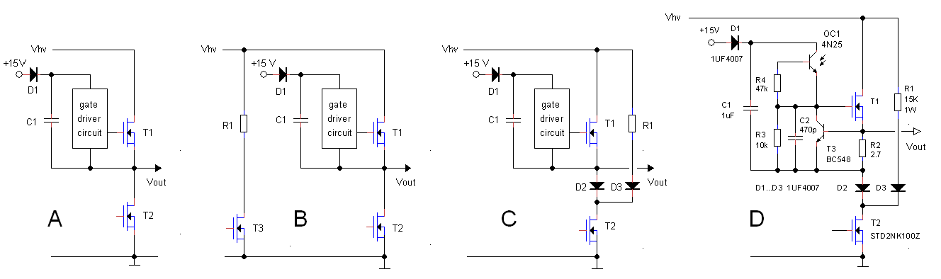
Figure 3.1 Circuit configurations for the high voltage switch.
Just like in the uTracer3, the gate driver circuit is powered from a capacitor that is charged immediately before the measurement pulse. Figure 3.1A schematically shows the idea. Before each measurement pulse T2 is briefly closed, which charges C1 to 15V. Next T2 opens again leaving the high voltage switch circuit completely floating and only connected to the high-voltage source.
We should almost forget that also a means to discharge the capacitors needs to be implemented to discharge the capacitors when e.g. a new curve is measured of when the measurement is finished. The simplest way to implement this is to use a simple discharge resistor and tranistor in the same way as this is done in the uTracer3 (Fig. 3.1B) However, it seems rather a waste to use an additional transistor for that while we have another high voltage switch in almost the same ôpositionö doing nothing most of the time: transistor T1 only needs to be closed a few milliseconds just before a measurement pulse! With a simple ôORö circuit consisting of diodes D2 and D3 we can have T2 perform the two tasks of discharging the reservoir capacitors and the grounding of high side driver circuit to charge the boots-trap capacitor.
Figure 3.1D shows a first attempt to an implementation of the high side gate driver circuit: R3 keeps T1 open when the transistor in the
opto-coupler is off. Transistor T3 and R2 form a simple current limiting circuit that is also used in the uTracer3, while C2 suppresses potential oscillations.
In the remainder of this section the high voltage switch will be analysed and tested to find out its operating limits.

Figure 3.2 Test circuit for the NMOS high voltage switch
Analzing and testing an ôhigh-sideö circuit like the high voltage switch is not that easy. All the components are at a high potential with respect to ground and complicated differential probes have to be used to measure e.g. the gate-source voltage of the switching transistor. Fortunately, since the control input of the switch is basically isolated from the rest of the circuit through the use of an opto-coupler (the bias diode D2 Fig. 3.2 is normally off), it is possible to exchange the position of the load and the switch with respect to ground so that the circuit can be tested using ground as a reference.
Figure 3.2 shows the test circuit used in this section. Going from left to right we first find a pulse generator which simulates the measurement pulse normally issues by the PIC. It consists of a de-bounce circuit around N1 and N2, the pulse generator consisting of C1, R3, D1 and N3, and a buffer that eventually drives the LED in the opto coupler consisting of N4-N7 and T1. The pulse length is determined by C1 and R3.
A 150 nF capacitor results in a pulse length of approximately 1 ms, the normal measurement pulse length. A 1 nF capacitor generates a 10 us wide pulse which is approximately the pulse width when the processor interrupts the measurement because an over-load condition has been detected. The reservoir capacitor consists of two 220 uF / 450 V capacitors in series. Resistors R6 and R7 ensure that the high voltage is distributed evenly over both capacitors. The current is measured over Rsense, which causes a negative voltage drop over the resistor. The reservoir capacitor is charged via R9 by my (very) high voltage supply consisting of three stacked delta E0300-0.1-L 0 ľ 300 V power supplies, capable of generating 0 ľ 900 V. The voltage over the high voltage switch is measured with a 10:1 voltage divider (and a 10:1 scope probe). The zener diode is used for Ron measurements to prevent overloading of the scope input.

The operation in detail
The high voltage switch can operate in three different modes:
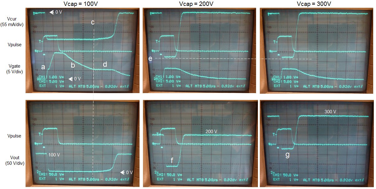
Figure 3.3 Analysis of the waveforms in the NMOS high voltage switch (see description below).
In Figure 3.3 the working of the switch in modes 2 and 3 is analyzed. For safety reasons the voltage is not pushed to the limit, but a maximum voltage of 300 V is used. The figure shows in three columns three different voltage setting: 100 V, 200 V and 300 V. The pictures in one column show different signals during the same measurement. The center trace in both pictures is the pulse signal that is also used to trigger the scope. In this case the pulse width is ca. 8 us. The upper trace in the top pictures shows Vcur which is the voltage drop over Rsense. The lower trace in the top pictures shows the gate voltage of the NMOS. The bottom trace in the lower picture shows the output voltage. Because the switch circuit has been shifted to ground level, the output voltage is high in the off-phase and should approach zero in the on-phase.
As load a resistor of 800 ohm is used. This means that with increasing voltage and the hardware current limit set at 250 mA (Rcur = 2.7 ohm), the hardware current limit protection will kick in at around V = R*I = 800*0.25 = 200 V. For 100 V the hardware current limit circuit is not yet activated. After the start of the measurement pulse, the photo transistor in the opto-coupler is switched on, and the gate voltage rises. The rise time is limited by the current the photo transistor can generate and the gate capacitance of the MOSFET. At Around 5 to 6 V gate voltage, the MOSFET switches on (Fig. 3.3a) and the output voltage drops. The sharp decrease of the anode voltage counter acts (through the drain-gate capacitance) the charging of the gate resulting in the kink in the gate voltage. Eventually the gate voltage rises to 15 V and the MOSFET is fully on. After the measurement pulse has been switched off, the gate is discharged by resistor R9 resulting in a logarithmic decay of the gate voltage (Fig. 3.3b). Since during that time the gate voltage is higher than the threshold voltage, the MOSFET remains fully on. At point c the gate voltage approaches the threshold voltage and the MOSFET starts being switched off causing an increase in anode voltage. The increasing drain voltage, again through the drain-gate capacitance, counter acts the discharging of the gate and actually stabilizes the gate voltage on a plateau value around the threshold voltage (Fig. 3.3d). At a certain point this balance situation can no longer be maintained and the MOSFET is finally switched off.
At 200 V the hardware current limit circuit has kicked in (Fig. 3.3 middle column). Note that the drain voltage in rest is 200 V, and but that during the measurement pulse the drain voltage is no longer zero but has increased to approximately 80 V (Fig. 3.3f). This is because the hardware current limit circuit has regulated the conduction of the MOSFET in such a way that it is now dropping these 80 V so that the current through the load remains constant at 250 mA. As a result, the gate voltage is adjusted to a value slightly above the threshold. Since the gate voltages is already around the threshold voltage, and the drain voltage is no longer zero, the switch-off time is drastically reduced. For 300 V the current remains constant (Fig. 3.3e), which is only possible by allowing for a higher voltage drop over the MOSFET (Fig. 3.3g).

Figure 3.4 Switching characteristics at Vgate = 15 V (left column) and Vgate = 10 V (right column).
Figure 3.4 shows a similar set of curves as in Fig. 3.3 for a voltage of 100 V and a load resistor of 800 ohm (current limit circuit not activated). In the left column a gate voltage of 15 V is compared to a gate voltage of 10 V in the right column. By decreasing the gate voltages the discharging of the gate is significantly reduces (comp. a1 to a2 in Fig. 3.4) However, the plateau time remains the same (comp. b1 and b2). A gate voltage of 10 V seems optimal.
Pulse testing @ 550 mA
During the first tests it appeared that the NMOS high voltage switch easily passed all load and short circuit tests with the hardware current limit set to 250 mA. The hardware current limit was therefore set to 550 mA by lowering Rcur to 1.189 ohm (2.7//2.7//10).
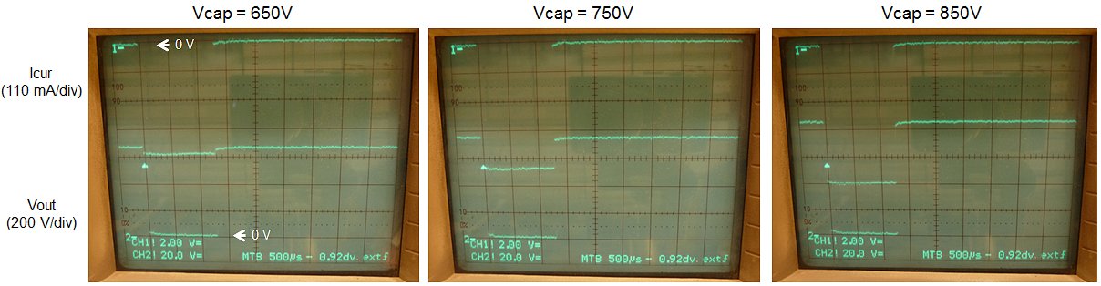
Figure 3.5 Mode 1 testing at 550 mA (load = 1k5).
The first test was for normal operation with a measurement pulse length of 1 ms. Figure 3.5 shows the current as well as the drain voltage of the switch connected to a load resistor of 1k5. The load resistor was chosen such that the current limit circuit would just come into action between 750 and 850 V. The graphs show a perfect switching behaviour even for the highest voltage and current combination.
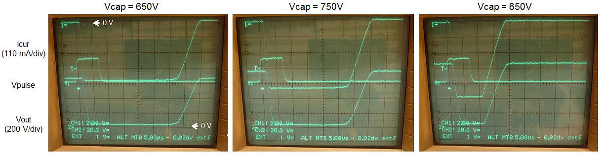
Figure 3.6 Mode 2 & 3 testing around 550 mA (load 1k5)
In the second test Mode 2 and 3 operation is simulated with a mesurment pulse length of 10 us. A load of 1k5 is connected and the voltage is increased from 650 to 850 V (Fig. 3.6). At 650 V the hardware current limit circuit is not yet activated, the gate voltage of the MOSFET of 15 V, and the turn-off time is relatively long. At 750 V the current limit circuit is just activated and the pulse length is decreasing. At 850 V the current limit circuit is fully activated, the gate voltage is around the threshold and the turn-off time is minimal. The current is 550 mA.

Figure 3.8 Full short circuit test at maximum voltage (850 V) and 550 mA! The tiny MOSFET in DPAK package is capable of handling an instantaneous dissipation of 425 W!
Finally a full short circuit test at maximum voltage (850 V) and maximum current (550 mA). Figure 3.8 shows how the tiny MOSFET handles an instantaneous dissipation of 425 W repeatedly without problems.
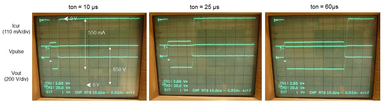
Figure 3.8 Exploring the safety margin
To investigate the safety margin we have with this switch circuit, the pulse length was increased in steps at maximum voltage (850 V) and full short circuit conditions (Fig. 3.8). It appeared that the pulse length could be increased to at least 60 us ľ 6 times the pulse length in reality ľ without problems. Most likely I could have gone further, but since this is evidence enough to convince me of the robustness of the circuit, and since I donĺt like pushing buttons and waiting for a bang, I didnĺt push it any further.
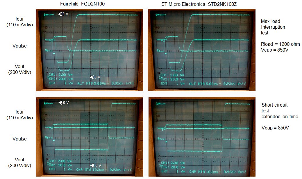
Figure 3.9 The FQD2N100 compared to the STD2NK100Z.
There are two 1000V MOSFETs that are readily available and reasonably priced: The FQD2N100 from Fairchild, and the STD2NK100Z from ST Micro Electronics. Their datasheets are pretty similar. The main difference is their price: the STD2NK100Z is about double the price of the FQD2N100. Under the assumption that more expensive also implies better performance all experiments so far were carried out using the STD2NK100Z. However, the comparison of the two in Fig. 3.9 shows that both transistors show almost identical behaviour and that FQD2N100 even shows slightly better turn-off characteristics.
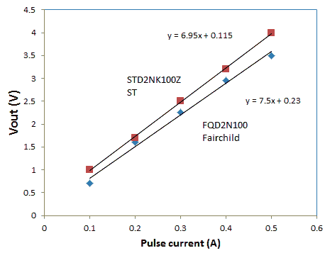
Figure 3.10 Voltage drop over the MOSFETs as a function of drain current.
The voltage drop over a bipolar transistor in saturation is usually more-or-less independent of the current, and usually amounts to 100 to 200 mV. A MOSFET in the on-state in contrast behaves as a resistor with the on-resistance a function of the gate voltage. The voltage drop over the MOSFET will therefor depend on the current. This is not a problem, since ľ just as with the uTracer3 ľ the plotted current can be corrected for this voltage drop. To measure the on-resistance of the MOSFET, the voltage drop over the MOSFET (+ 2.7 ohm resistor) was measured for different currents taking care that the current limit circuit was not activated. To measure the Ron, the output voltage of the output voltage divider was limited to 2.7 V by means of zener diode D3 (Fig. 3.2). This allows for zooming into the low voltage drop when the MOSFET is on, while the input voltage is clipped when the MOSFET is off so that the amplifier of the oscilloscope is not saturated. The Ron (corrected for the 2.7 ohm resistor) has been plotted versus the current for both type MOSFETs in Fig. 3.10. The on-resistances for both types are indeed more or less constant and correspond well to the values specified in the datasheets.

A small personal souvenir of a fantastic holiday in the Yorkshire Dales: a panoramic view on Middleham from Williamĺs Hill.
Tackling dV/dt breakdown
While playing with the HV-switch test circuit (Fig. 3.1) a rather startling incident/accident occurred. I had the load resistor connected with two (isolated) clips, and at a certain moment I disconnected the load while the reservoir capacitor was charged to 900 V and T3 was not conducting. The moment I opened the clip, there was a big bang and the MOSFET, Rcur, Rsense, and a fuse I had in series with the capacitor were blown to pieces (Fig. 4.2)! What on earth had happened, and how can opening of a circuit result in such a violent event?
The most likely explanation is a dV/dt breakdown. Such a breakdown can occur when the rate of increase of the drain voltage exceeds a certain value. What happens is that the drain-gate capacitance causes a positive transient on the gate which not only momentarily opens the MOSFET, but which also may very well destroy the gate oxide causing the MOSFET to permanently fail. When I opened the clip I must have accidentally touched the lead resulting in a dV/dt breakdown.
One of the most effective measures to prevent dV/dt breakdown is to lower the impedance of the circuit that is driving the gate of the switching transistor. In the driver circuit shown in Fig. 4.1 the gate of the MOSFET in the off-state is connected to ground via a relatively high value 10k resistor. The lower the resistor value, the smaller the voltage spike on the gate. A simple push-pull buffer will drastically lower the impedance level and significantly reduce the sensitivity to dV/dt breakdown.
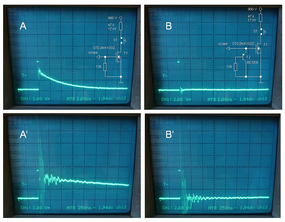
Figure 4.1 dV/dt testing without gate driver circuit (AAĺ) and with push-pull gate driver (BBĺ).
A simple experiment was used to get an qualitative idea of the impact of a buffer circuit on the dV/dt fenomenon. In Fig. 4.1A the drain of the MOSFET is connected via a push button and a current limiting resistor to a 900 V power supply. The signal on the gate of the MOSFET is monitored with a memory scope. When the switch is closed a transient appears om the gate. Figure 4.1Aĺ shows the same event on a different time scale. An extra transistor acting as an emitter follower almost completely suppresses the transient (Fig. 4.1B and Bĺ). At t=0 there is in all cases a very large and very short spike that doesnĺt decrease in amplitude when a buffer is used. I think is has nothing to do with the dV/dt effect but is just a measurement artifact.
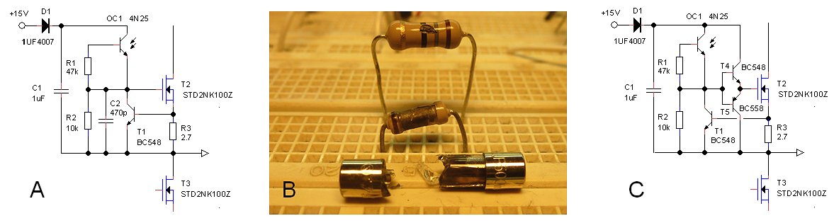
Figure 4.2 A) Original HV-switch circuit, B) collateral damage as a result of a dV/dt breakdown, C) new HV-switch circuit with gate driver.
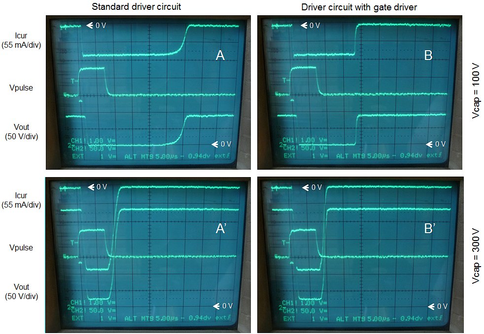
Figure 4.3 Switching behavior of the new HV-switch circuit compared to the standard circuit. Rload = 1 kohm
In the HV-switch circuit shown in Fig. 4.2C, a push-pull buffer circuit has been added to provide a low impedance drive circuit for the gate of the MOSFET. This does add some complexity to the circuit, but it greatly suppressed dV/dt related problems, while it also improves the switching speed of the circuit especially the turn-off time. This is illustrated in Figure 4.3. Here the switching behavior of the standard circuit (left two phortos) is compared to the circuit with the buffer stage (right two photos). In the top two photos the hardware current limit is not activated, while it is activated in the bottom two measurements. Especially in the case when the current limit is not active the reduction of the switch-off time is significant because the discharge of the gate-source capacitor is faster (Figure 3.3 part a1). However, the typical MOSFET turn-off behavior/time when the gate voltage passes through the Vt (Fig. 3.3 part b1) still remains.
Pulse testing @ 1 A!
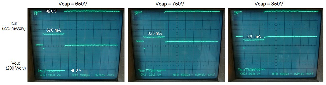
Figure 4.4 Standard 1 ms test. Rload = 900 ohm (1k//10k), Rsense = 2.7/4 = 0.65 ohm
During experiments with the HV-switch with the push-pull gate driver it was observed that the new circuit was much more stable in the current limiting regime. The 470 pF capacitor could be omitted without any problems and only for very low voltages oscillations were observed which readily disappeared for voltages higher than 100 V. It was therefore decided to again test the circuits up to currents of 1 Ampere! To set the hardware current limit to 1 A , Rsense was replaced by four 2.7 ohm resistors in parallel. Figure 4.4 shows the one millisecond Mode 1 test for voltages and currents around the maximum values. With a load resistor of 900 ohm and a voltage of 850 V, the circuit is tested at maximum voltage and maximum current. At the highest current the discharging of the reservoir capacitor is clearly visible
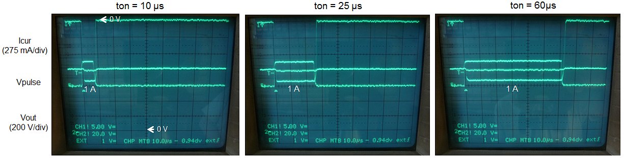
Figure 4.5 Full short circuit test extended times. Rsense = 2.7/4 = 0.65 ohm
Figure 4.5 Shows the high-speed switching behavior around the current limit region. The switching of 1 Amp at 900 V is no problem at all for the circuit. The switching speed is very fast, and the total on-time is very much determined by the control pulse width.
Finally, the robustness of the circuit was tested under full short circuit conditions at maximum voltage for extended times. The circuit easily managed to cope with repeated blasts at 60 us without problems!
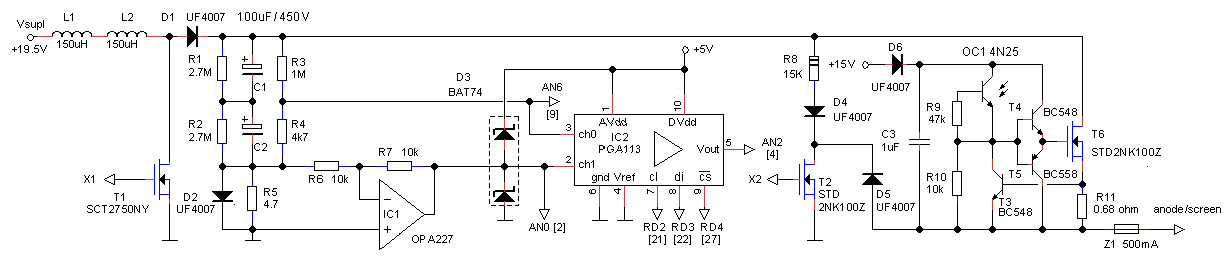
Figure 4.6 First version of a 1000 V/1 A anode & screen supply
Figure 4.6 Shows a first draft of the new anode/screen supplies. After the previous sections the circuit holds no surprizes. On the left hand side the circuit around T1 forms the 1000 V boost converter, assuming that in the end 500 V capacitors are used. The current sense resistor has been dimensioned to give a voltage drop of 4.7 V at a current of 1 A. The high voltage divider also (approximately) outputs 4.7 V at the maximum voltage of 1000 V. Note that for R3 a 1000 V type needs to be used. In contrast to the uTracer3, the high voltage feedback is not only fed directly into the ADC input of the PIC, but also to the free input of the PGA. I am considering to use the PGA during the setting of the voltage to increase the resolution especially at lower voltages. The BAT86 diodes that were used in the uTracer3 have been replaced by a single Schottky overvoltage protection pair D3 because under certain circumstances the output of the IC1 can swing to -15 or +15 V. The high voltage switch around T6 is identical to the circuit discussed in this section. As explained in Fig. 3.1D T2 has the double function to discharge C1 and C2 when needed, but also to charge C3 immediately prior to a measurement. Finally, not shown in this schematic, T1 and T2 need to be driven by a separate driver buffer because their gate voltages are not compatible with the output voltages of the processor.
Although the grid bias circuit of the uTracer3 - considering its simplicity - works quite well, I nevertheless wanted to revise the circuit for the uTracer6. Over the years many people have expressed wishes or made suggestions for improvements. I have summarized the most commonly made suggestions below:
Obviously, I have been thinking about a circuit that would be able cover the complete wish list stated above. However, unavoidably every time I ended up with a complex circuit that completely spoilt the concept of the uTracer: an elegant circuit designed to balance the thin line between complexity and performance. A circuit covering all the requirements would add excessive complexity and cost, while 95% of the users only need the basic functionality.
In the end I decided on a circuit that realizes only the basic requirements: range 0 to -100 V, high accuracy over the complete bias range, and current sinking capability. However, the specials such as an extended negative bias range or positive biases can be realized by the addition of an optional extension circuit to be realized as a ôshieldö that can be simply clicked onto the main board by users that require the additional functionality.
The basic circuit
A complicating factor in the grid bias circuit is that, just as in the uTracer3, the cathode of the tube is referenced to the positive power supply voltage, nominally 19.5 V. This implies that also the grid voltage needs to be referenced to the positive power supply voltage. Just as in the uTracer3 this is done by using an OpAmp configured as a subtraction circuit. Figure 5.1A shows the OpAmp subtraction circuit in its most general form. In most versions of this circuit R1=R2 and R3=R4, while R3=A*R1 (Fig. 5.1B). The result is a circuit that amplifies the voltage difference between the two terminals A times. Not so often used is the variant shown in Fig. 5.1 C. Here R1=R4 and R2=R3, while R2=A*R1. In this case the output voltage is the voltage on the positive input minus A times the voltage on the negative input. When the positive input is connected to the cathode and the output of the OpAmp to the grid, a voltage Vadc on the input will result in a grid bias of ľA*Vadc.
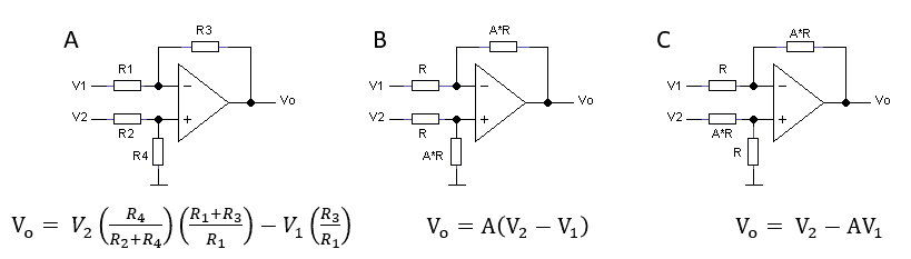
Figure 5.1 The OpAmp subtraction circuit in its general from (A), and two special cases (A & B).
The trick is that for the uTracer6 a very special OpAmp is used: the LTC6090 from linear technology, now Analog Devices I believe. This remarkable device has a supply voltage range of 140 V! It has a rail-to-rail output, is unity gain stable, has on chip temperature protection and an output disable input and it comes in a small SO8 package. By connecting the positive supply voltage input to the 19.5 V supply voltage and the negative supply voltage input to a voltage of at least -80 V, a grid voltage range of 0 to -100 V with current sinking capability can be realized. Figure 5.2 depicts the circuit in its elementary form. An AD converter controlled by the PIC generates a voltage of 0 to 5V. By setting the gain of the subtraction circuit to 200/10 = 20, a 0 V ADC output voltage corresponds to 0 V grid voltage while a 5 V ADC voltage corresponds to a grid voltage of -20*5 = -100 V.
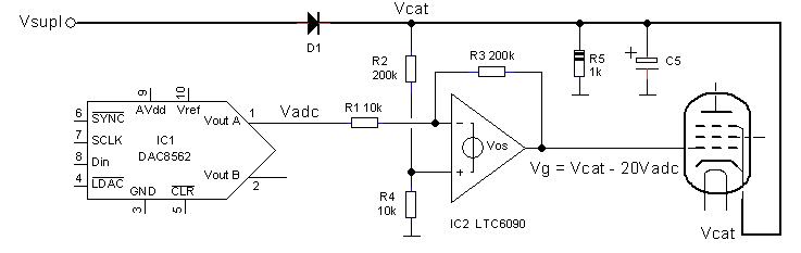
Figure 5.2 The principle of the grid bias circuit of the uTracer6.
Offset voltages
One thing to consider is the offset voltage of the LTC6090. From the datasheet of the LTC6090 we learn that the typical input offset voltage of the device is specified as 0.33 mV, while it can be as high as 1.2 mV. With a gain of 20 this can result in an offset voltage at the output ranging from 6.6 mV to 24 mV, excluding offsets introduced by tolerances in the resistors, the ADC and other preceding stages. Unfortunately, the LTC6090 is not provided with an input to compensate for the offset voltage. However, it appears possible to compensate for the input offset by deliberately creating a small imbalance in the resistors of the subtraction circuit:

The imbalance in the resistors can easily be created for instance by tweaking R4. Taking a peek forward to Figure 5.3, we see that placing a high value resistor in parallel to R4 first lowers its value slightly which can then be compensated for with a low value potentiometer. Placing a 2M7 resistor over the 10 kohm resistor and using a 10 turn 100 ohm potentiometer makes the resultant resistance variable between 9.963 kohm and 10.063 kohm. Inserting these values in the equations above results in a δ of approximately ± 0.005. With a supply voltage of 19.5 V this will result in offset correction range at the output of the OpAmp of approximately ± 100 mV.
The complete circuit
Figure 5.3 shows the complete grid bias circuit as I have it in mind for the uTracer6. Going from the left to the right, we first find the inverting boost converter that is used to generate the -85 V voltage that is used for the negative supply voltage of the LTC6090. The circuit is based on the inverting boost converter of the uTracer3, but in this case the pnp BC138 transistor has been replaced by the readily available 100V PMOS transistor IRFR9120. Just like the other boost converters in the circuit, also this boost converter is controlled by the PIC microcontroller. The firmware was originally designed so that it can handle up to 8 boost converters simultaneously (read
here and
here). This not only greatly simplifies the circuit, but it also gives the PIC total control over the boost converters. One of the ôtricksö in the uTracer is that all boost converters are shut down during the 1 ms measurement interval, thereby greatly eliminating the noise in the circuit.
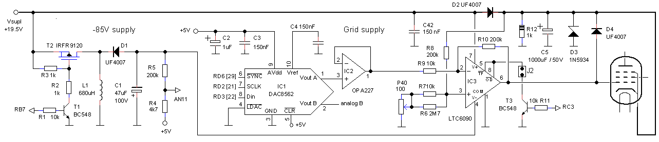
Figure 5.3 The complete ôbasic versionö grid bias circuit.
For the DA converter I selected the DAC8562 from Texas Instruments. The DAC8562 houses in a tiny MSOP package two independent 16-bit DA converters, a voltage reference and an SPI control. I have used one of the two DA converters for the negative grid supply, while the other DA converter is reserved for the positive grid supply. Since a 16 bit word is used to control the grid voltage, positive and negative, this implies that both converters will be used in 15 bit mode. With 15 bits the resolution is then set to 100V/2^15 = 100V/32768 = 3.1 mV. The ôzero code errorö of the DAC8562 is specified as typically 1 mV (max 4 mV). However, when the DAC was directly connected to the subtraction circuit, the zero code output voltage appeared to be much higher since the DAC output had to sink the current through R9 (approximately 100 uA). To completely decouple the DAC from the subtraction circuit, buffer IC2 was added.
The subtraction circuit itself has already been discussed, however there are a few particulars worth mentioning. From the beginning I was a bit worried about the dissipation in the LTC6090. With such high supply voltages already a small current either in the form of current used by the OpAmp itself, or current supplied to the output can result in a relatively high dissipation and associated temperature increase. For this reason, the package has been supplied with a thermal pad on the backside that can be used to transfer heat from the chip inside to the PCB. For hobbyists not in the possession of SMD soldering equipment, handling a package with a thermal pad can be a bit of a nuisance. Therefore I wanted to avoid the use of the thermal pas all together. The idea was to activate the output of the LTC6090 only during the actual measurement pulse, while I hoped that the dissipation of the LTC6090 itself would be low enough to avoid excessive heating of the package.
The LTC6090 has an output disable input on pin 8. When this pin is pulled low, the output of the LTC6090 basically goes into tristate mode. Normally the output disable input is tied to the temperature flag output (pin 5). This open drain output pulls the output disable pin low when the internal temperature of the LTC6090 reaches a certain critical point. In the grid bias circuit, the collector of transistor T3 is or-tied to the output disable input. This transistor is controlled by the PIC, and only switches the output of IC3 on during the actual measurement. T3 is connected to the output disable pin with a jumper. The jumper can be removed so that the output is switched on continuously to facilitate testing and calibration. In practice it turned out that the dissipation in the LTC6090 is not a problem at all.
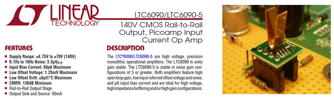
Figure 5.4 During the experimental phase of the circuit development the thermal pad of the LTC6090 (here lying on its back) was provided with a small copper heatsink. This turned out to be not necessary.
Diodes D2, D3, D4 as well as C5 and R12 protect the circuit in the case of a flashover from anode to grid or cathode (read more here). When a flashover occurs the excess amount of charge is stored in C5. As a result, the voltage over C5 will increase. Diode D2 now isolates the cathode from the rest of the circuit. In case the potential rises above 24V, diode D3 will start to conduct and short circuit the charge to ground. Diode D4 directs flash overs to the grid to the cathode. Resistor R12 serves the purpose to maintain a constant current through D2, while it also discharges C5 during/after a flash over. Notice that the positive power supply voltage of the LTC6090 has been taken from the anode side of D2. Although the OpAmp is advertised as rail-to-rail, in reality there is (as with most OpAmps) always a few hundred millivolts of difference between the maximum output voltage and the positive supply voltage. The 0.6 V voltage drop over the permanently forward biased diode neatly compensates for this so that the grid voltage can be really adjusted to zero volt.
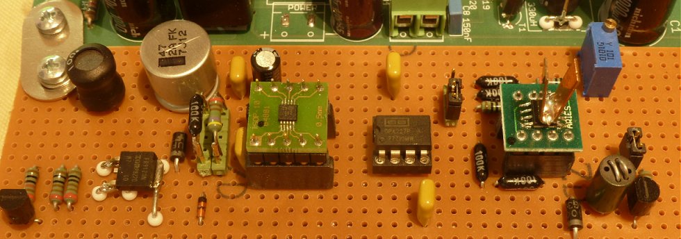
Figure 5.5 The complete grid bias circuit on perf board.
Obviously the new grid circuit does require necessary but not very exciting modifications to the firmware in the PIC, as well as to the GUI. For the calibration the DAC is loaded with zero which should result in a zero-volt grid voltage with respect to the cathode. With the potentiometer the output can now be set to exactly zero. It appears that during the first 20 min after switch on of the circuit there is a small drift in the grid voltage (about 20 mV), it is therefore recommended to wait at least 20 min before performing the zero grid voltage calibration. The full scale calibration is performed during the final calibration of the uTracer in the GUI.
Few aspects of the uTracer3 have been such a point of discussion as the heater supply and the ôold fashionedö RS232 interface. I am afraid that for the uTracer6 I am going to stick with the same concepts, but with a big improvement in the heater supply. In this section a motivation and an explanation.
The Heater supply (alternatives)
During the design of the original uTracer, I added the heater supply as a ônice to have add-on.ö I had one PWM output on the PIC left and thought it would be a nice idea to use it to make a simple PWM controlled heater supply. Readers who are interested in the full story of the heater supply and its short comings can read up here and here. On this page I will just suffice with a short summary.
The heater is driven by a PWM circuit that switches the heater output at a high frequency between the supply voltage (19.5 V) and ground. Because of the thermal inertia of the heater, the effective voltage on the heater settles to the rms value of the PWM signal. The energy supplied to the heater can simply be regulated by varying the duty cycle of the PWM signal. In principle this is a nice and elegant idea, however, unfortunately in the uTracer3 the repetition frequency of the PWM signal was rather high namely 19.5 kHz. The reason for this is that the other PWM module in the PIC processor is used to generate the grid bias. Here a high frequency makes it easier to low-pass filter the signal to get a DC voltage. The problem now is that as a result of the high PWM frequency, the PWM pulses become very short for low heater voltages. These narrow pulses in combination with (parasitic) inductances in the wiring degrade the rectangular shape of the short pulses (see measurements below), which results in a somewhat lower effective heater voltage than expected.
The problem in short is not that the circuit concept is not sound, but rather that the PWM frequency is too high. In the uTracer6 there is no need for that anymore. Since the grid bias is no longer generated by the second PWM output but by a proper DAC, a much lower frequency for the PWM repetition frequency for the heater can be chosen. The result is much wider PWM pulses that are far less sensitive to parasitic inductances.
Over time I have collected quite en extensive wish list for the heater circuit of a new uTracer. The list includes: higher voltages (up to 100 V), higher currents, higher accuracy, the possibility to monitor the heater current, etc. Apart from the whish for a higher accuracy, I have to disappoint everybody. I have thought about it quite a lot and even experimented with modern buck converter solutions. However, I have found that it really is impossible to compete with the many ready-made power supply solutions that are on the market today.
|
|
|
|
Figure 6.1 Some ready-made power supply modules that depending on your wishes and budget can be an attractive alternative for the built in heater supply of the uTracer6. Click on a picture to execute a search for the specific module.
Quite a few users of the uTracer3 who found that the internal heater supply of the uTracer3 didnĺt satisfy their needs have discovered the world of cheap and ready-made power supply solutions. Albert Valiente made his own 35 V / 9 A heater supply from a display module, a pre-assembled buck converter and a ten-turn potentiometer. Read his description here. Other users have combined the uTracer with a completely ready-made power supply module
(e.g.
Example1
,
Example2
,
Example3
,
Example4
,
).
A Google search on ôvariable power supply module,ö yields pages full of all kinds of power supplies that can be ordered for only a few euro. Figure 6.1 shows some of the more prominent results at the time of writing of this page. To be honest, it simply doesnĺt make sense to try to compete with this with an elaborate programmable heater supply for the uTracer6. So there we have it, I think that the improved heater circuit of the uTracer6 will serve the needs of 80% of the users; the other 20% are far better served with a ready-made solution that additionally offers the possibility to pre-heat tubes without the necessity of a computer connection.
Evaluation of the improved heater circuit
Now that the second PWM output is no longer used to control the grid bias, we can choose any frequency for the heater PWM. The frequency of the PWM generators is controlled by Timer 2 of the PIC. With a crystal frequency of 20 MHz it is possible to set the frequency of the PWM generator to 1.22 kHz, 4.90 kHz, 19.53 kHz by changing the setting of the clock prescaler to 16, 4, 1 respectively. For the uTracer6 I choose to go down to 1.22 kHz.
In the uTracer3 the gate of the MOSFET is driven by a bipolar push-pull pair in order to obtain as steep as possible gate pulse, to reduce switching losses. At a 10 times lower frequency, the switching losses are negligible so it was possible to eliminate the complete push-pull stage and even to introduce a gate series resistance to limit the gate current.
The first thing to check is if the lower PWM frequency indeed makes the heater supply less sensitive (or even insensitive) to parasitic inductances in the wiring.
The first thing checked was the shape of the PWM pulses. The top row of figures in the Fig. 6.2 depicts the shape of the PWM pulses applied to an EL34 heater at a PWM frequency of 19.53 kHz. Note that the reference of the oscilloscope is connected to the positive power supply voltage, so that a low signal means that the voltage is applied to the heater. Going from left to right, respectively 0, 3 and 5 RFI suppressions beads were inserted in series with the heater leads, each RFI bead adding 25 uH (test setup in Fig. 6.5 right). Observe that with only a little bit of inductance the square pulse shape is heavily distorted, resulting in a too low effective rms heater voltage. In the bottom row graphs the PWM frequency is lowered to 1.22 kHz. Obviously also in this case the trailing and leading edges of the PWM pulses are distorted, however, because the frequency is so much lower that has little to none effect on the total pulse shape. Even with 10 bead in series the pulse wave shape is nearly perfectly rectangular.
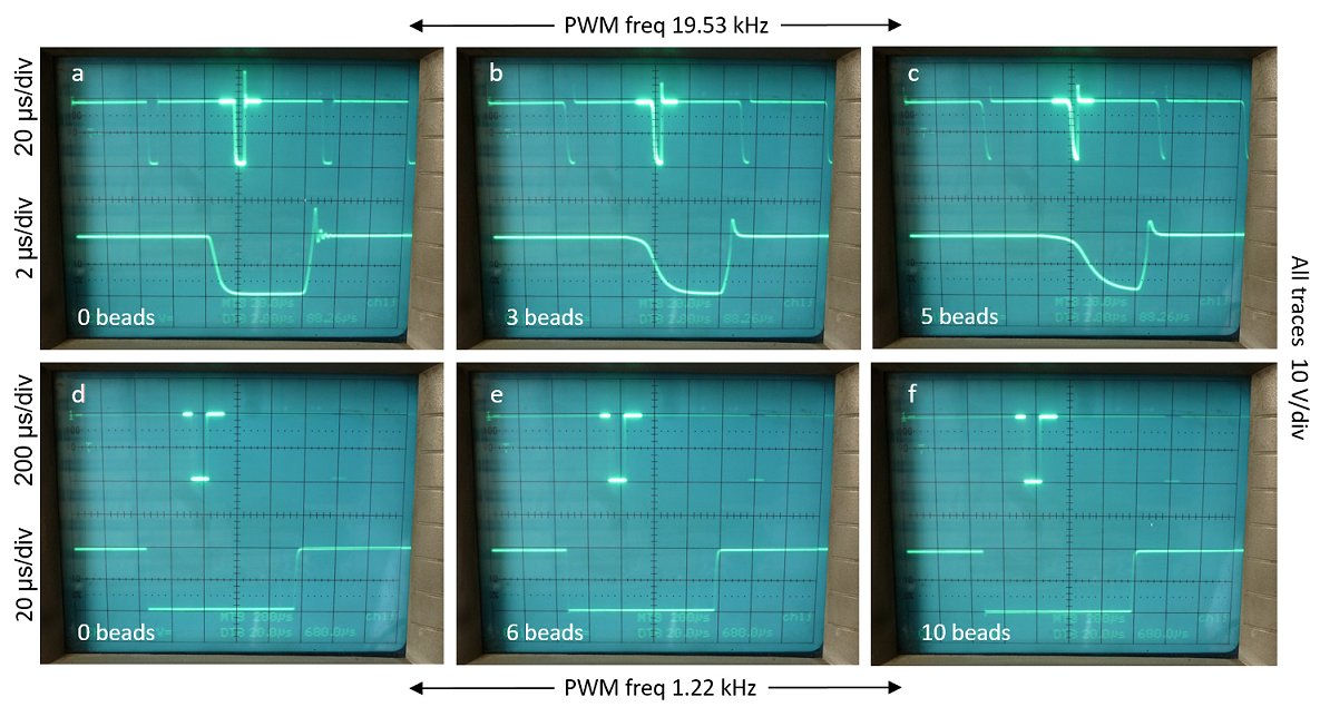
Figure 6.2 Comparison of the effect of parasitic series inductance on the pulse shape of the PWM heater supply for two different PWM frequencies. Each bead introduces 25 uH.
It is not at all straightforward to directly measure the equivalent rms voltage generated by the heater supply. Even multimeters that that can provide true rms AC measurements fail to give accurate results. The problem is the very high ôcrest factorö of PWM signals for either very low or very high duty cycles. The crest factor is defined as the peak amplitude of a waveform divided by its rms value. For a PWM signal with fixed amplitude and 10 bits resolution, the crest factor can be as high as sqrt(1000)=30! I own a professional Keithley model 2000 multimeter that is capable of true rms measurements, but even for this instrument the accuracy is not even specified for crest factors higher than 5! No wonder it produces absolute nonsense for high and low duty cycles. The best accuracy can be expected when the duty cycle is approximately 50%.
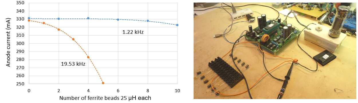
Figure 6.3 Effect of parasitic heater series inductance on the anode current of an EL34 at fixed bias conditions for two different PWM frequencies (left). Test setup with a first peek preview of an experimental uTracer6 (right).
The easiest way to quantify the rms heater voltage is to measure the effect on the anode current for fixed anode, screen and grid voltages. Figure 6.3 left shows the anode current of an EL34 at Vg = -1 V, Va = 300 V, and Vs = 275 V for the two PWM frequencies with different number of 25 uH inductors beads in series with the heater leads. The graph clearly shows that except for very large series inductances, the anode current and thus the effective heater voltage is more or less independent of parasitic inductances.
As long as the PWM pulses are nicely rectangular and not distorted, there is a simple way to directly measure the rms value of the heater supply, provided that you own a good old analog multimeter! Analog multimeters measure the average voltage of an AC signal, and when the waveform is known - in this case a PWM signal with nice rectangular pulses - there is a direct relation between the average voltage of the signal and its rms value. To understand that we need a little bit of theory.
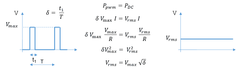
Figure 6.4 The rms voltage of a PWM modulated signal.
The formulas on the left hand side of the equal sign in Fig 6.4 give the effective power delivered to a resistor R by a PWM supply with duty cycle δ and amplitude Vmax. This should be equal to the power supplied to the same resistor by a DC supply with an equivalent voltage Vrms. The bottom equation then shows the relation between the rms voltage of the PWM supply and its parameters Vmax and duty cycle.
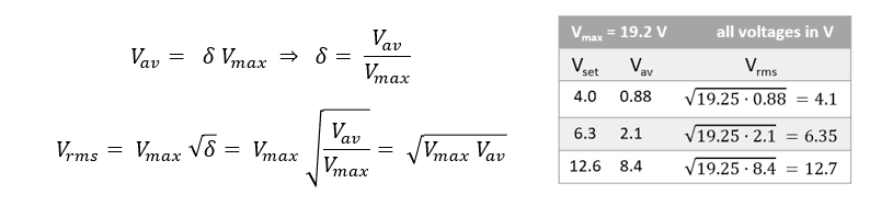
Figure 6.5 The rms voltage of a perfect PWM signal as a function of average voltage and maximum voltage.
The average value of a PWM signal as measured by an ôold fashionedö multimeter is simply Vmax times the duty cycle δ (Fig. 6.5). Substituting δ into the equation of Fig. 6.4 yields Vrms as a function of the average voltage and Vmax, the supply voltage. The table in Fig. 6.5 lists the in this way measured rms heater voltage for three different GUI settings delivered to a 100 ohm resistor. The values are slightly higher that the set points, but that is due to the fact that I never bother to calibrate my experimental uTracers.
Figure 6.6 Left, I own two UNIGOR multimeters from the 60ĺs / 70ĺs. They are in perfect working order, indestructible and I use them for everything! Right, FDTI TTL-232R-5V cable interface on an experimental uTracer6.
The RS232 interface
I fully realize that everybody these days is used to appliances and applications that you can just plug into your USB port, and that simply make a connection and then work (most of the times). Unfortunately, that is not so simple for amateur and semi-professional projects and products. I started this sections three times over trying to explain why, but in the end I decided to just give a list of arguments why I want to stick to the ôgood old (fashioned)ö RS232 interface:
A small enhancement I will make is that I will provide for a connector that also provides a +5 V power supply voltage to accommodate Bluetooth modules etc. and a connector that can be used to directly connect a TTL-232R-5V cable from FDTI (Fig.6.6).

Large part of this section was written during a weekend out to The Hague.
There we visited a memorable exhibition of the Dutch painter Louis Apol at the panorama Mesdag museum.
Reading through these sections it might perhaps seem that this has been a single straight path adventure. That is obviously not the case. There have been many trials and errors and considerations whereby the most difficult part has been to find the balance between something that is ôdoableö for the amateur and that at the same time gives unprecedented performance. I have already mentioned that after a few ôwildö experiments with the uTracer4 and the never published uTracer5, I decided to stay close to home and use the uTracer3 as the skeleton to build on the uTracer6. This is nicely illustrated by Fig. 7.1. Eurocircuits my trusted supplier of PCBs from time to time sends me some extra PCBĺs. These come in very handy in experiments! The half populated uTracer3 PCB in combination with the perfboard PCB on the left of Fig. 7.1 first was used to test the different high voltage boost and flyback converter ideas using the original grid bias supply. Next, the perfboard to the right was added with the new grid bias circuit. Finally, the new negative supplies and new heater supply were implemented and tested.
Figure 7.1 Very first test version of the uTracer6. click here to view the bottom side of the PCB.
Figure 7.2 shows the analog circuitry of the uTracer6 while Fig. 7.3 shows the microcontroller and some miscellaneous circuitry. Letĺs go through the circuit diagram section by section to start with the most interesting part, the analog circuit. To make it easier to trace a certain component in the circuit diagram and on the PCB, the components have been numbered into groups. Components numbers 1-19 belong to the general section, components 20-39 are part of the negative power supply, components 40-69 belong to the grid bias supply while numbers 60-79 belong to the anode supply. Finally, components 70-99 are part of the screen supply.
Starting at the lower left corner of the Fig. 7.2 we first find the heater supply which has been reduced to a single transistor T4. With the lower PWM frequency (see section 6), the gate driver stage included in the uTracer3 was no longer necessary. The IPD048N06L3 that was selected for T4 has a low enough Vt so that is can be directly driven from the PIC. Moving to the right we find two almost identical circuits that generate the negative supply voltages in the circuit, -15 V and -85 V. The circuits are pretty much similar to the negative supply circuit of the uTracer3 except for the fact that the pnp transistor has been replaced by a modern PMOS transistor the IRFR9120. Whereas in the uTracer3 an LM337 was used to regulate the -15V, in the uTracer6 this voltage is directly regulated by the inverting boost converter itself. Moving even further to the right we find the power supply input. A so called ôfools diodeö D1 shortens the power supply input to protect the circuit when the plus and minus of the power supple are accidentally interchanged. Next the power supply is split into a ôclean partö that e.g. feeds the grid section, and a ôdirty branchö that feeds all the switch mode power supplies. The dirty branch is filtered by a heavy choke L1 and C15.
Moving one row up, R5 and R6 form a voltage divider that reduce the supply voltage to a level so that it can be sampled by one of the PICĺs ADCs. The software uses this information amongst others to calculate the correct duty cycle for the heater supply. Moving to the right we find the positive power supplies consisting of two standard linear regulators. Note that the input voltage from the +5 V regulator is taken from the output of the +15 V regulator to distribute the dissipation over the two regulators. Compared to the uTracer3 the +5 V regulator does not heat up noticeably.
Moving further to the right we find the grid bias supply. Compared to the uTracer3 this part of the circuit has been completely redesigned. Central to the grid supply is the DAC8562 DA converter. The DAC8562 houses two independent 16 bit DAC converters and a voltage reference. The whole chip is controlled through a standard SPI interface. For the uTracer6 really a 14 bit DA would have been sufficient, but is appears that the DAC8562ĺs 14 bit sister (the DAC8162) is more expensive than the 16 bit version (!). The outputs of the DAC8562 are practically rail to rail with 0 V output for code 0000H programmed. During experiments it appeared however that the modest load of the IC42 output stage is enough to lift the zero code output voltage of the DAC8562 by a few millivolts, enough to cause a few tens of millivolts of offset at the grid output. Since this time I really wanted to have a consistent grid supply that would really go to 0 V, buffers IC41 a and b were inserted to isolate the DAC from the output stage. Of the two DACs inside the DAC8562 one is used for the negative grid bias supply, while the other one is reserved for the positive grid supply so it is routed to the extension connector.
Figure 7.2 Analog section of the uTracer6.
For an extensive description of the grid output stage the reader is referred to the one of the previous sections. Identical to the uTracer3, the cathode of the tube is connected to the positive power supply (through diode D40). This means that the 0 to 5 V output voltage of the DAC has to be translated to a 0 to -100 V grid voltage with respect to cathode (positive power supply). For the output stage the LTC6090 is used. This high voltage OpAmp can be used with a differential supply voltage of up to 140 V. In this circuit the positive supply voltage is connected to the cathode (positive power supple voltage), while the negative power supply voltage is connected to the -85 V power supply. The difference of 20 ľ (-85V) = 105 V is enough for a 100 V grid bias supply range with 5 V headroom left. The output of the LTC6090 can swing to about 100 mV from the positive power supply line (@ 1mA). Therefor the LTC6090 is connected to the anode side of D40. The 600 mV introduced by this diode guarantees that the grid voltage can really go up to 0 V.
A few more components in the grid circuit need explaining. The offset compensation circuit around P40 has already been discussed in section 5. The LTC6090 has an output disable input pin. When this input, which has an internal pull up, is pulled to ground, the output of the LTC6090 is disabled. This greatly reduces the dissipation. Normally this pin is connected to the open drain temperature flag output. When the internal temperature of the LTC6090 becomes too high, this pin pulls the disable pin to ground to protect the OpAmp for overheating. In the uTracer6 this pin is additionally connected to the collector of T40. In standy T40 conducts, thereby disabling the output. Only during the actually measurement pulse itself the output of the LTC6090 is enabled. With this precaution it is not necessary to use the nasty thermal pad underneath the LTC6090. When jumper J2 is removed, the output of the LTC6090 is enabled continuously. This is needed when the calibration phase the offset is adjusted with P40.
The remaining components in the grid section R46, C44, D41, D42 protect the circuit during a flash over from anode (or screen) to cathode or grid. During a flash over, the excess charge is dumped in C44. When the voltage of C44 becomes too high, D42 starts to conduct dissipating the excess energy. R46 discharges C44 when needed, and provides a continuous current through D40. Diode 41 diverts a flash over from the grid to the cathode to protect the LTC6090. Although these safety measures have proven to be quite effective in the uTracer3, it is never possible to protect the circuit for all possible calamities. It is therefore recommended to be cautious with ôunknownö tubes, and preferable always perform a gas and short test on a regular robust tube tester. Please keep in mind that the uTracer foremost is a curve tracer, not a go / no-go tester!
Moving up we find the screen and anode supplies. These have already been extensively discussed in sections 2, 3, and 4. The only modification here is that the current sense OpAmp is now configured as a subtraction circuit instead of just an inverting amplifier. The addition of two 10k resistors greatly reduced the influence of spurious common mode signals. The default current sense resistor is 4.7 ohm. This will allow for currents of up to 1A to be measured over the 0 to 5 V input range of the PGA. It is not difficult to see that the high voltage divider circuits (R63/R64 & R83/R84) have been dimensioned in such a way that it can handle voltages up to 1000V. For R63 and R83 special high voltage SMD chip resistors were used. Just as in the uTracer3, the output of the high voltage divider is directly connected to one of the ADC inputs of the PIC, However, it is also connected to the second so far unused input of the PGAs. If needed, this will make it possible to increase the resolution at lower anode/screen voltages. However, this will require some fast switching between the two inputs of the PGAs and I am not sure if I will use this option.
Figure 7.3 Digital section of the uTracer6.
Compared to the analog part of the circuit, the digital part is pretty straightforward (Fig. 7.3). At the centre of the circuit is the 16F844 microcontroller. This is the recommended replacement for the 16F874A that was used in the uTracer3. The 16F874A is slowly being taken out of production and ônot recommended for new designsö anymore. I get a continuous stream of emails regarding the choice of processor. I know there are more ômodernö solutions that offer a wealth of additional features. The reason for me to stick with this processor is that the firmware, which is written in assembler, and which is very much intertwined with the hardware, has proven to work very well and reliable. My mistake with the uTracers4 and 5, which never made it into a working prototypes, is that I wanted to change too many things at the same time and for a one-man job, which basically has to be done in the evening hours, this is not a good idea. So I stick to the 16F844 running with practically the same firmware as was used in the uTracer3 (see next section).
To the left of the processor we find the standard RS232 interface. Owners of a uTracer3 can directly plug the RS232 connector of their uTracer3 into pin header A. People who want to use the popular TTL-232R-5V USB cable from FDTI can plug it directly into connector C (read more here). Finally, those of you who want to experiment with alternative interfaces, such as Bluetooth modules, can use connector C, which offers the serial interfac at TTL levels and a +5 V power supply connection. When either connector B or C is used, the MAX232 needs to be removed from its socket!
The SCT2750NY SIC transistors and the high voltage 2NK100Z MosFets have a relatively high Vt so they cannot be driven directly from the PIC processor. Instead the very common gate driver IR25600 is used to bring the gate signals to power supply voltage levels. Attentive readers may have wondered why the LEDs in the two opto couplers are driven by two separate transistors (T1 and T2). The very simple reason is that in this way it was easier to retain the symmetry in the layout of the PCB.
On the right side of the PIC we find the connector for the extension board, which in first place is intended for the positive grid supply, but that also can be used for other extension options. The table below lists the meaning of the pins on the extension connector.
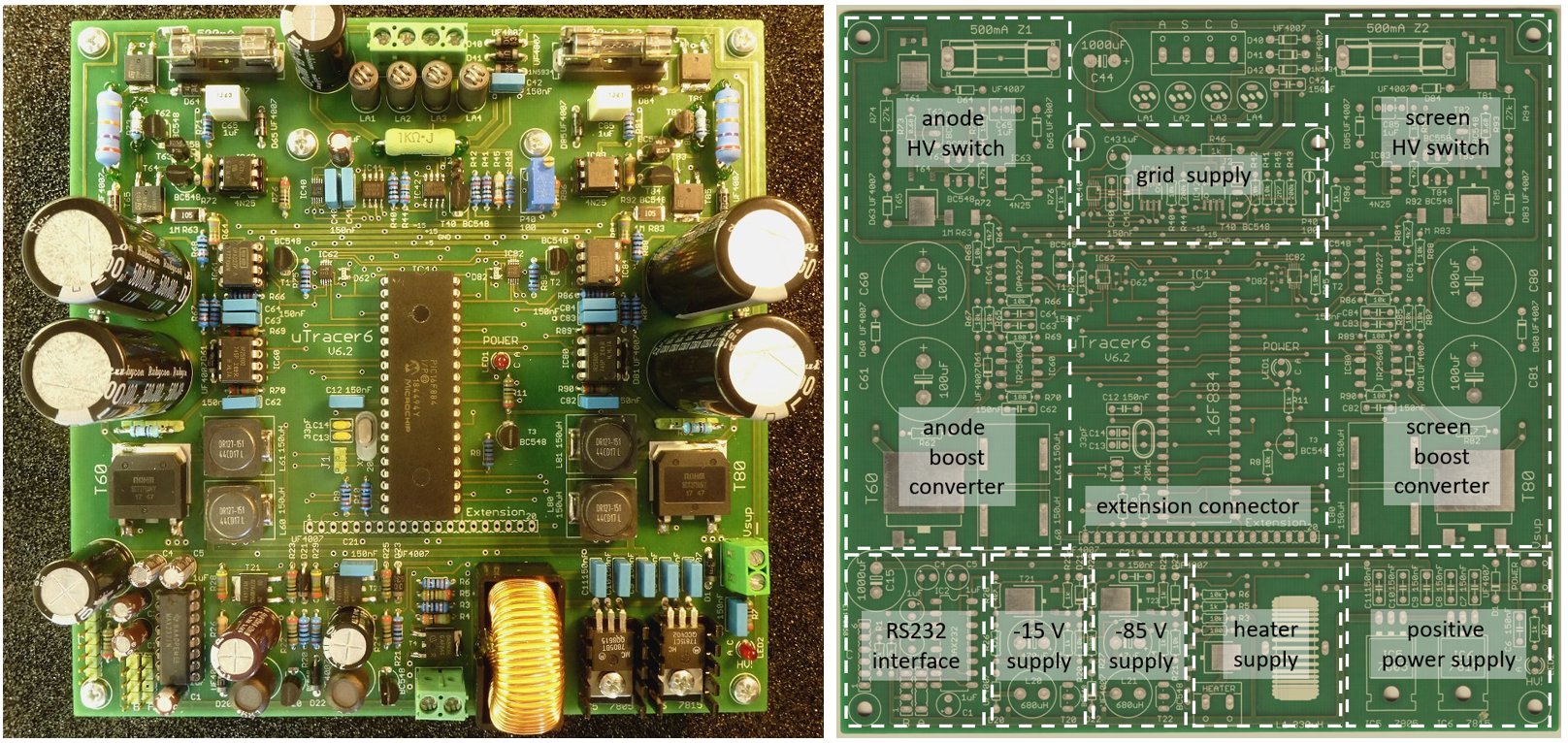
Figure 7.4 The PCB of the uTracer6 after three iterations
I very rarely design PCBs, so again also this time it was again quite an adventure to dive into an old version of Eagle I bought years ago and get going. For myself it is very important that a PCB is aesthetically pleasing. For me symmetry is very important! So I spend quite a bit of time shifting components over the board until I came to a design that I liked. Figure 7.4 shows the almost final version of the PCB for the uTracer6. A special design constraint was that at in some parts of the circuit we have to deal with high voltages (up to 1000 V), which requires a somewhat spacious design. In the centre of the board, space is reserved for the extension board ôshield.ö Both the anode and the screen high voltage sections can be found on the left and right side of the PCB. The circuits appear to be completely mirrored, but to make this possible, many of the active components had to be rotated by 180 degrees! The dimensions of the board are exactly 6x6 inch, or 152.4x152.4 mm.
Figure 7.5 First measurements with the uTracer6.
Nr
Connection
Description
1
-15 V
-15 V power supply for analog electronics
2
Vcat
Cathode potential reference
3
+19.5 V
+19.5 raw power supply
4
+19.5 V
idem
5
RC0
Universal digital I/O, normally pulled up by a 10k resistor
6
RC1
idem
7
RD1
Measurement pulse strobe, active high
8
Analog B
Buffered second output of the grid DAC
9
RA4
Universal digital I/O
10
+5 V
+5 V power supply
Nr
Connection
Description
11
0 V
ground
12
RC3
grid enable, becomes low before the measurement pulse, active low
13
-85 V
-85 power supply
14
RD2
Serial peripheral interface, clock
15
RD3
Serial peripheral interface, data
16
RB6
Digital output for positive grid power supply boost pulse
17
RB3/AN9
Analog input to measure voltage of the positive grid supply
18
RB0/AN12
Analog input reserved for measuring the grid current
19
RD7
Universal digital I/O
20
+15 V
+15 V power supply for analog electronics
The command and result strings.
The communication with the uTracer is via a serial RS232 link at a speed of 9600 baud, 8 bits, no parity, and one stop bit. The commands to the uTracer are given in the form of a string of 28 (Uppercase) ASCII characters. Each character sent to the uTracer is immediately echoed. Failure to echo a character represents a malfunction of the uTracer.
Every two consecutive characters in the ASCII string represent an eight bit byte. The first byte is the command code. The following 8 bytes represent data. Different formats for the data are used depending on the command code, however in most cases the eight bytes are grouped into four 16 bit words representing the anode voltage, the screen voltage, the grid voltage and the filament voltage.
Some strings do not result in a response from the uTracer. Other strings result in the uTracer sending a result string. The result string also has a fixed format, and consists of 38 ASCII characters. Again every two consecutive characters in the ASCII string represent an eight bit byte.
The first byte is the status byte which signals if the command to which the result string was a response was executed successfully. The remaining 18 bytes represent data grouped into 9 two byte words. The format of the result string is fixed (Fig. 8.2).
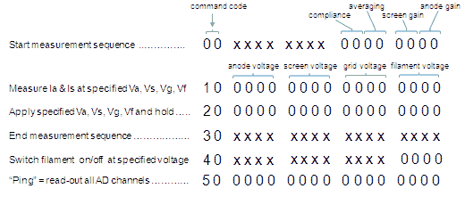
Figure 8.1 Definition of the Command Strings.
The data in both the command string as well as in the result string is always in 10 bits binary format. This means that the upper 6 bits of the data word are not used. These bits should be zero. In most cases the binary data directly represents a 10 bit result of the on-chip AD converter, or a setting of the 10 bit on-chip PWM modulator. All conversion of for the user meaningful numbers to and fro binary representations is done in the GUI. In this way a minimum amount of intelligence is needed in the micro-controller.
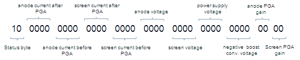
Figure 8.2 Structure of the Result String
Structure of a complete measurement sequence
The different commands should be send in a certain order, although sending the commands in a random will not result in an error. The preferred command sequence is shown in Fig. 8.3. When the ôHeater Onö command is pressed, the GUI send a ôSet Settingsö (<00>) command followed by a ôPingö (<50>) command to obtain the current supply voltage. It then sends ôSwitch On Heaterö (<40>) command. The only thing this command does is to copy the last word of this command to the filament PWM generator. The other words should be ô0000ö. The filament
voltage can be directly set to the final value or the GUI can generate a ôsoft-startupö by issuing a sequence of <40> commands with increasing filament voltage values. The uTracer does not send a response after receiving a <40> command
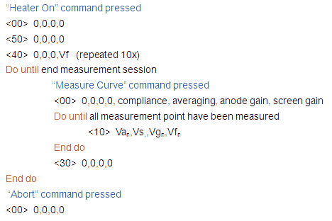
Figure 8.3 Structure of a typical Measurement Session
While the filament is heating, the user has the time to select a measurement type on the GUI and to set the proper measurement conditions. When next the user presses the ôMeasure Curveö button, the sequence to measure a set of curves is started. The first command issued is the <00> ôSend Settingsö command. This command transfers the gain settings for the anode and screen amplifiers, the required number of average measurements and the current compliance value. There is no response of the uTracer to the <00> command. Next the GUI starts issuing <10> ôDo Measurementö commands. The four words in the command exactly specify the anode, screen, grid and filament voltages. After reception of the command the uTracer sets all the specified bias conditions and performs the measurement. The result is communicated back to the utracer in a result string. The value of the status byte indicates if the measurement was successful. If the status byte = 10H everything is ok, a value of 11H indicates a compliance issue on one of the two channels. The GUI can issue any number of <10> commands. At the end of a measurement sequence the GUI issues the <30> ôEnd Measurementö command. This command discharges the high voltage buffer capacitors and set the grid voltage to zero. In the same measurement session more curves or a different type of curve can be measured by repeating the <00>,<10><10><10>ů.,<30> sequence. At the end of the session the filament voltage is switched off by issuing a <40> command with a specified filament of zero volt.
The format of the variables
In this section the format of the variables that are used in the communication with the uTracer will be defined. Some of these variables are one byte, while other variables use two bytes (a word).
anode and screen gain
The anode and screen gain variable is only one byte long, and used both in the <00> command string, as well as in the result string. In the command string it is used to specify the gain of the anode or screen current amplifiers, or to specify that the ôauto gain/rangeö option is selected. In the return string the variable returns the actual gain as it was determined by the ôauto rangeö algorithm in the uTracer and used for the current measurement point. The lower nibble directly reflects the gain convention as it is used by the PGA113: 00H=1X, 01H=2X, 02H=5X, 03H=10X, 04H=20X, 05H=50X, 06H=100X, 07H=200X. In addition code 08H is used to indicate that the auto-gain algorithm has to be used.
cThe average variable is one byte long. The variable is only used in the <00> command string. In principle the variable can have any value in between 1 and 32 (001H and 20H). In practice only the values 1, 2, 4, 8, 16 and 32 are used. This is because the user can only choose from these values. When the variable has the value 40H it indicates that the auto-averaging algorithm has to be used
compliance
The compliance variable is one byte long and only used in the <00> string. The variable defines the voltage of the on-chip voltage reference which is compared by the two on-chip comparators to the voltage drop over the current sense resistors. When the voltage drop over the resistor exceeds the reference voltage, the measurement is aborted. The value of the compliance variable is directly copied into the CPU register which controls the voltage reference: CVRCON.

Since the voltage reference has to be enabled (CVREN=1) and disconnected from the output pins (CVROE=0) the highest two bits of the variable have to be always 10xxxxxx. VCRR defines the measurement range while the lowest nibble of the variable selects the tap in the resistive ladder network. When the variable has for example the value 10001111=8FH a 200 mA compliance has been selected (see also section 14).
anode and screen voltages
The term anode and screen voltages in the context of the variable description is rather misleading since the variables not so much specify the anode and screen voltages itself but rather the voltages of the anode and screen buffer capacitors. It will be recalled that the cathode of the tube is referenced to the power-supply voltage of 19.5 volt so that there is also an offset of 19.5 V between the voltage of the buffer capacitor and e.g. the anode voltage. To be more precise the anode (screen) voltage is the voltage of the anode (screen) buffer capacitor minus 19.5 V. The voltage of the buffer capacitor is measured using a resistive voltage divider so that a 0-1000 V range is mapped on a 0-5 V range. The conversion formulas which give the relation between variable n and the high voltage(s) are:
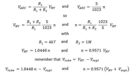
The anode and screen voltages variables occupy two words and are used both in the command as well as in the result string. Since a 10 bit AD converter is used, only the lower 10 bits of the two bytes are used. The variable n in these equations can have any value between 0 and 1023.
anode and screen currents
The anode and screen currents are measured from the voltage drop they cause over a current sense resistor of 4.7 ohm. When so needed the voltage drop is first amplified by a Programmable Gain Amplifier (PGA) before being fed into the AD converter. When an averaging larger than 1X is used, the uTracer just adds the measurements to the variable which is transferred to the GUI. The GUI subsequently performs the floating point division. The relation between the variable n, and the anode/screen currents (in Amps) is given by:
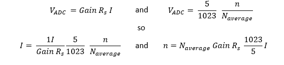
The anode and screen current variables occupy two words and are only used in the result string. Although only a 10 bit AD converter is used, the variable can use the full two byte word of 16 bits for 32X averages. Two values that are also returned are the anode and screen currents before the PGA. In other words, the voltage directly over the current sense resistors (after inversion). This value is not used by the GUI. The conversion formulas are identical to the equations above with Gain=1 and Average=1.
power supply voltage
The power supply voltage is measured because it is an important parameter in the calculation of the settings for the proper filament voltage. It is only used in the return string. Like the high voltages, the power supply voltage is simply measured using a simple resistive voltage divider consisting of R5 and R6 (Fig. 7.2).
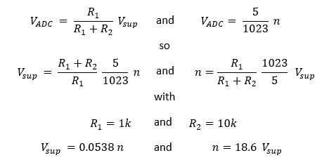
control grid voltage
With the new control grid circuit, also the communication protocol with the uTracer has been completely changed. The protocol was defined in such a way that in the future also positive grid bias values can be handled. The protocol now covers the range of -100V to +100V. The mapping is defied in such a way that 0 to -100V is mapped on 0000H to 7FFFH, and 0 to +100V is mapped on 0000H to 8FFFH. So the full 16 bits of the DAC are used to cover a range of 200 V resulting in a resolution of 200/65.536 = 3.1 mV.
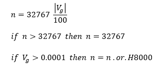
filament voltage
Also the filament voltage is controlled by a 16 bit word which is only used in the command string. The word is directly used to program one of the on-chip PWM circuits. The PWM circuit is set at a repetition frequency of 19.5 kHz, when the variable is zero the duty cycle is also zero and the filament voltage is zero. When the variable is 03FFH, the duty cycle is 100% resulting in a filament voltage equal to the supply voltage. There is a quadratic relation between the effective filament voltage and the duty-cycle (d). The relation between the variable (n) and the filament voltage is given by:
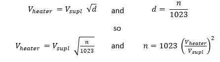
negative boost converter voltage
The negative boost converter voltage is not a variable which is set by the GUI, but rather it is specified during the initialization of the firmware to a fixed value of -40 V. The relation between the variable (n) and the negative boost converter voltage (Vboost < 0) is given by:
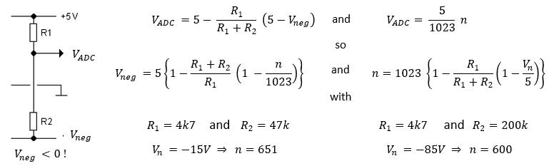
The software in a project like this is not particularly the most interesting part, but it cannot be avoided. This section is probably the most boring contribution to this weblog so far, but the write-up is needed, mainly because these pages also serve as my own documentation and if I donĺt write things now down, it will take me ages to puzzle things together at a later stage. This section will cover three topics:
Migrating from the 16F874A to 16F844
As already mentioned in one of the previous sections, the 16F874A that was used in the uTracer3 is slowly becoming obsolete (and expensive!). Microchip recommends the 16F884 as a pin and (almost) software compatible alternative. Again, I know that there are much more modern, faster, fanciful new processors, but if there is one thing that I have learned over the years it is that the time I have to put in a project like this - next to a pretty busy job ľ is limited. Since the uTracer3 firmware has proven to work quite well in over 1500 uTracers, I decided to make small incremental steps and take the uTracer3 firmware as a starting point. This approach worked very well and it allowed me to realize the uTracer6 step-by-step without having to start from scratch all over.
This section basically describes the modifications in the firmware necessary to migrate from the 16F874A to the 16F884 so that it can be used in the uTracer3. In the other subsections firmware modifications will be discussed that are particular to the uTracer6. The 16F884 is very similar to the 16F874A, but nevertheless a number of modifications in the firmware had to be made. A good starting point was the migration note available on the Microchip website. Below a list of the modifications that were necessary. In the assembler input file these changes are labelled in the comments with @#16F884.
          16F874           16F884

        7654 3210         76543210
 AN0    1000 0001  81     1000 0001  81
 AN1    1000 1001  89     1000 0101  85
 AN2    1001 0001  91     1000 1001  89
 AN3    1001 1001  99     1000 1101  8D
 AN4    1010 0001  A1     1001 0001  91
 AN5    1010 1001  A9     1001 0101  95
 AN6    1011 0001  B1     1001 1001  99
 AN7    1011 1001  B9     1001 1101  9D
 AN8                      1010 0001  A1
 AN9                      1010 0101  A5
 AN10                     1010 1001  A9
 AN11                     1010 1101  AD
uTracer6 specific modifications
In this subsection the changes in the uTracer3 firmware are listed that were necessary to adapt it to the uTracer6 hardware.
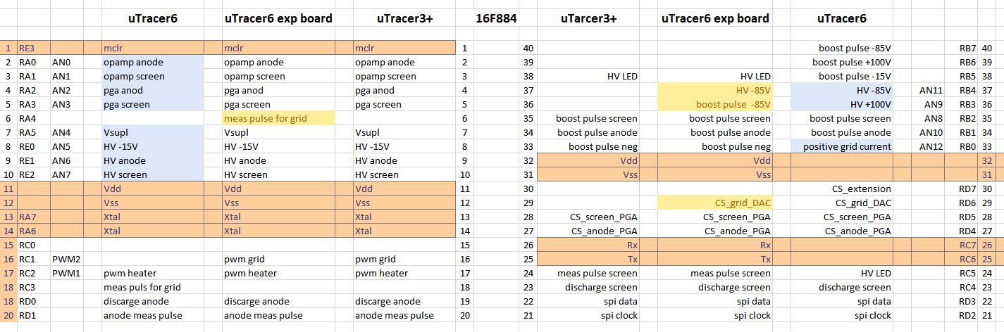
Figure 9.1 pin assignment of the PIC in the uTracer3, the experimental version of the uTracer6 (see Fig.7.1), and the final uTracer6.
Discharge control
After each measurement the 100 uF high voltage reservoir capacitors of the uTracer need to be discharged to bring the circuit in a safe state, and to prepare it for a new measurement. The way this was implemented in the uTracer3 had two shortcomings:
First a new flag was introduced named ôDISCHARGE.ö Not surprisingly when this flag is set, the outputs which control the discharging of the high voltage caps are made high. Remember that every 100 us, the discharging outputs are made low by the interrupt service routine that controls the boost converters, so that for discharging the main program needs to set the outputs continuously until the caps are discharged!
In the uTracer3 the stopping of the discharging was coupled to the HV-LED. In the uTracer6 I wanted to decouple this and be able to stop the discharging independently from the status of the HV_LED. To make this possible a new routine ôCHK_DISSö was made that compares the measured anode and screen voltages against two threshold values. When both the anode as well as the screen voltages are below the threshold values, the DISCHARGE flag is reset. Note that the routine cannot set the flag, only reset. By the way, comparing 16 bit words with a PIC is not completely trivial, but with the help of this document I once found on internet it was pretty straightforward.
DISCHARGE:=true
DO WHILE (DISCHARGE=true) OR (NOT_-15V_OK) OR (NOT_-85V_OK)
call chk_diss Ĺthis routine resets the discharge flag if both anode and screen voltage are below a threshold value
IF DISCHARGE=true THEN
set discharging on
ELSE
set discharging off
ENDIF
END DO
After power-up the uTracer firmware now follows the pseudo code listed above. First, by default, the DISCHARGE flag is set. Next the program enters a loop that is only exited when the capacitors are discharged and when both negative power supplies have come on-line. In the loop the capacitors are checked and the discharge outputs are continuously set as long as the caps are not discharged. Next the program enters the main program loop:
DO FOREVER Ĺthis is the main program loop
Ĺ
DO WHILE no_newchar_received Ĺwait for a new received character in buffer
call chk_diss Ĺthis routine resets the discharge flag if both anode and screen voltage are below a threshold value
IF DISCHARGE=true THEN
set discharging on
ELSE
set discharging off
ENDIF
END DO
Ĺ
call receive_command Ĺreceive command and process it
IF the_command_requires_high_voltages THEN
DISCHARGE:=false
ENDIF
IF command=end_of_measurment THEN
DISCHARGE:= true
ELSE
execute command
ENDIF
Ĺ
END DO
The main program loop first waits until a new character is received. While it is waiting, it discharges the capacitors if needed as described above. The loop checks if a new character is received by polling the RCIF flag in the PIR1 register. This flag is set as soon as a new character has been received and placed in the buffer. When indeed a new character has been received, the command is processed even if the capacitors are not fully discharged yet!. Only when a command was received that requires a high voltage, the discharging is stopped by resetting both DISCHARGE, as well as the discharge outputs.
öThe case of the blinking HV-LEDö
Most users of the uTracer will have noticed the short blinking of the HV-LED when the high voltage caps are almost discharged. To understand the origin of the problem it is important to understand how the HV-LED is controlled. In order for it to reflect the true momentary status of the high voltage caps, in needs to be updated continuously. This is done by incorporating the LED control routine in the interrupt service routine that controls the boost converters, which is called every 100 us (read more here). Since the interrupt service routine controls 4 boost converters (5 when the +100V grid option will be added) the actual anode and screen capacitor voltages are measured every 400 us (500 us).
The origin of the blinking LED lies in the fact that the discharging of the high voltage caps is linked to the status of the high voltage LED, and that the on and off switching of the high voltage LED algorithm does not have a hysteresis. So as soon as the voltage of the caps reaches the point where the LED is switched off, also the discharging stops. If now for some reason, e.g. because of parasitic inductance of the electrolytic caps the voltage fluctuates a little bit, the LED will start blinking until the caps are sufficiently discharged by the resistive voltage divider used to measure the voltage. In the previous subsection I explained how the discharging was decoupled from the status of the LED, in this subsection hysteresis will be added to the LED control.
In order not to waste any machine cycles in the interrupt service routine, a ôdirty trickö is used to determine if the capacitor voltages are below or above a certain threshold value. It is simply done by checking the value of the highest bits of the 10-bit AD converter result:
The HV-LED is switched on  when the highest 4 bits of either the anode or the screen voltages are NOT ZERO (> 63*1.0448 = 65.8V)
The HV-LED is switched off when the highest 5 bits of both the anode and screen voltages are ZERO  (< 31*1.0448 = 32.4V)
So the LED is switched on when either the anode or the screen cap is charged to 66V, and it is only switched off when they are both discharged to a value below 32V. After this the discharging continues to the value set for the discharge routine, 24V. A final thing to consider is that during the actual measurement pulse calls to the interrupt service routine are stopped. This is to make the circuit absolutely ôquietö during the actual measurement of the currents and voltages. When after the measurement pulse the interrupt service routine is enabled again, it will take at least 4 calls, so approximately 0.5 ms before the variables that contains the actual anode and screen voltages are updated. During that time the status of the LED should not change. This is arranged by the flag ôLEDFLAGö which is controlled in the main program which sets the flag 0.5 ms after the interrupt service routine has been enabled. All this results in an algorithm given by the following piece of pseudo code that can be coded with only a few AND and OR instructions:
IF LEDFLAG = true THEN
   IF LED = off THEN
       IF .NOT. highest 4 bits of measured voltages zero THEN
             LED := on
       ENDIF
   ENDIF
   IF LED = on THEN
       IF highest 5 bits of measured voltages zero THEN
             LED := off
       ENDIF
   ENDIF
ENDIF
Low voltage accuracy
One of the consequences of the very simple circuit topography of the boost converters in the anode and screen supplies is that for very low anode and screen voltages there is an inherent inaccuracy in the setting of the voltages. For the measurement itself that does not matter, since the exact voltages are accurately measured during the measurement pulse, regardless of the set-point value.
The origin of ôthe problemö is related to the way the boost converters are implemented. The heart of the boost converter is an inductor that during a time t - the charge pulse - is connected to the supply voltage. During that time the current in the inductor increases linearly. At the end of the charge pulse the current in the inductor has increased to I = (t*Vsupl)/L, and the stored energy equals 0.5(L*I^2). After the charge pulse has ended the inductor dumps this energy in the high voltage electrolytic capacitor so that its voltage increases to accommodate the extra energy. The amount of energy delivered in each package is every time the same and defined by the pulse length (and of course the supply voltage and the inductance value). The whole process is repeated at a rate of 10 kHz. After every four pulses the PIC measures the voltage of the capacitor and when the voltage is higher than the set-point value the pulsing stops (read more here)
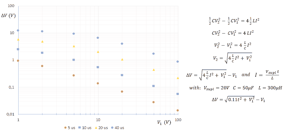
Figure 9.2 Left: voltage increment per four charge pulses as a function of capacitor voltage and pulse length (Vsupl=20V, C=50uF, L=300uH). Right: the equations.
The formulas on the right hand side of Fig.9.2 mathematically reflect this process. The final formula gives the increment per charge pulse depending on the voltage of the capacitor. It is clear that when the capacitor is completely discharged, the increments are largest. As the voltage of the capacitor increases, the increments become smaller and smaller. So inherently the set point voltage of the capacitor is less well controlled for lower voltages. The only parameter that we can play with to increase the accuracy is the charge pulse width. A shorter pulse results in less charges stored in the inductor and hence a smaller increment. However, a shorter charge pulse will at the same time increase the charge time at higher voltages.
So, on one hand we want to keep the charge pulses short to more accurately control the charging of the capacitors, while on the other hand we want to have them as long as possible to quickly charge the caps to high voltages. The maximum pulse length that can be used before the inductors go into saturation is 40 us. The graph on the left hand side of Fig. 9.2 shows the voltage increment per four charge pulses as a function of the capacitor voltage for four different charge pulse widths. From the graph it can be seen that even with a charge pulse length of 40 us, the increments quickly drop below 1 V for voltages higher than 100 V. In reality they will be even less due to losses in the circuit.
Figure 9.3 Left: charging 0-100 V with 40 us charge pulses. Right: idem with 10 us charge pulses.
To make a long story short, in the uTracer6 firmware a provision has been implemented that selects either a short charge pulse of 10 us when the set-point is below a certain threshold value, or the maximum pulse length of 40 us when the set-point is above the threshold (changes labelled with @#IC). The threshold values for the anode and screen supplies can be set individually, but for now they have been set to 100 V for both. Even with this provision, the voltage control is not perfect at voltages below say 100 V. It should be noted that the 0 ľ 100 V range is mapped to 0 ľ 0.5 V on the ADC input. During the charging of the capacitors there will be quite some noise in the circuit due to the boost converters. This will certainly effect the setting of the capacitor voltages, especially in the low voltage region. However, as mentioned, during the actual measurement pulse, the boost converters are switched off so that the voltage measured during the actual measurement will be accurate.

This section was written during a nice and quiet holiday in Terhofstede behind the Dutch coast. The picture shows a view from the beach in Holland across ôhet Zwinö with in the distance Belgiumĺs best-known and most affluent seaside resort Knokke. Download a beautiful extensive article about the history and restauration of ôhet Zwinö here (in English).
The first line of this page promises the uTracer6 to be a 1000 V / 1000 mA curve tracer, and it is! But as usual there is more to the story than just this statement. Many people will not need the full 1000 mA current range, and in that case it is possible to optimize the uTracer6 for the type of tubes you are interested in. To do that you need to understand a little about how the uTracer works.

Figure 10.1 Simplified circuit diagram of the current sense and limit circuit of the uTracer.
General working
Figure 10.1 shows a greatly simplified circuit diagram of the core of the measurement circuit of the uTracer. In principle the working is very simple. A boost converter (not shown) charges capacitor C1 to the desired anode voltage. When the set point is reached, switch (transistor) T1 closes for a millisecond, allowing an anode (or screen) current to flow.
Current measurement
The current causes a voltage drop -Rs*Ia over the current sense resistor Rs. Verify for yourself that this voltage drop, which is obviously also a pulse, is negative with respect to ground. The amplitude of the pulse is proportional to the current. Since the ADC in the PIC can only handle positive voltages, the negative voltage drop over Rs is inverted by OpAmp A1 so that we find a positive pulse with amplitude Rs*Ia at the output of A1. The PIC microcontroller samples this voltage during the measurement pulse and converts it to a 10-bit number. The software in the GUI finally converts this number back into a current. Since the ADC has an input voltage range of 0 to +5V, this implies that at Imax - the maximum current we want to measure - the voltage drop has to be equal, or less than +5V, so Rs ≤ 5 / Imax. So for a maximum current of 1 A, Rs ≤ 5 / 1 = 5 ohm. As a safe and practical value 4.7 ohm has been used in the uTracer6.
It should be realized that, unless we make the circuit very complex and expensive, there is always a trade-off between maximum current range, and accuracy at lower currents. The higher the maximum current, the smaller the voltage drop over Rs and the more this voltage drop, which can become very small, has to compete with noise and imperfections of the circuit. With a current sense resistor of 4.7 ohm for example, a current of 1 mA corresponds to a voltage drop of only 4.7 mV, making it for the circuit hard to eliminate the influence of noise etc. So if you do not need the full 1A current range, you should consider increasing Rs to accommodate the current range you need. The GUI allows you to specify the value of the current sense resistors that you use so that you can tailor the uTracer6 to your needs.
Compliance
Unfortunately, the story is a little bit more complicated because we also have to consider the mechanisms that have been installed to limit the current. These are the compliance, a software mechanism, and the hard current limit, a hardware mechanism. The first line of defence is the compliance circuit. The compliance circuit uses the comparator and programmable voltage source modules provided in the PIC (Fig. 10.1). During the measurement pulse the amplitude of the voltage drop over the current sense resistor Rs*Ia is compared to a reference voltage. As soon as the voltage drop exceeds the reference voltage, an interrupt is generated and T1 is switched off. This mechanism actually works quite fast. On average it takes only 10 us for the PIC to switch off the output(s) when a too high current is detected.
The snag here is that the on-board voltage reference source can only generate voltages as high as 3.6V (donĺt ask me why). This means that with a 4.7 ohm current sense resistor the highest current that can be measured before the compliance circuit kicks in is I = V/Rs = 3.6/4.7 = 766 mA. So how do we go from here? The choice is up to you, basically there are three options:
Hard current limit
The final line of defence against over current situations is the ôhard current limit.ö The compliance mechanism described above is nothing more than a provision that switches off the outputs as soon as the current exceeds a certain value. Despite that it is reasonably fast, worst case currents can still increase to very high values, for example in case one of the outputs is short circuited. The hard current limiter limits the current in these situations. The hard current limit circuit is very simple and consists of a single transistor (T2) and resistor (RL). The working is very simple. As soon as the voltage drop over RL exceeds the voltage at which T2 starts to conduct, approximately 0.6 V, transistor T2 will pinch-off the high voltage switch T1. This means that whereas in the compliance circuit the output transistor is simply switched off and none of the components get stressed, in this case the output transistor is forced in a state somewhere between fully on and fully off meaning that (part of) the power is now dissipated in T1. In case of a complete short circuit this could be as high as 1 kW!! Obviously this situation should not last for very long, and hopefully the compliance circuit will have switched off the output before any damage to the transistor can occur.
From the above description it is clear that the hard current limit value (Ilimit) should be set to a value higher than the highest compliance value the user can select. Experimentally it was found that the proper resistance value for RL can be found from RL = 0.612 / Ilimit. In the standard uTracer6 configuration Rl = 0.56 ohm. This sets the hard current limit to 0.612 / 0.56 ≅ 1.1 A.
Users of the uTracer6 can configure the circuit to their own need, by simply changing the values of Rs and RL. Note that the selected value of Rs has to be entered in the proper fields in the calibration form so that the GUI knows how to calculate the right currents! Below some examples of configurations that are possible. Note that resistor values have been rounded to ôstandardö values, and that in all cases a 0.5 W or 1 W power rating is more than sufficient.
Some pictures
After all this text some pictures. All measurements below have been taken with the anode section in the maximum current configuration with RL = 0.56 ohm, Rs = 3.5 ohm (4.7//13.5), and the screen section with RL = 0.68 and Rs = 4.7 ohm (the anode and screen sections can be configured differently obviously). The captions below the pictures give further details.
Figure 10.2 In this measurement the anode terminal is connected with a 500 ohm resistor to the cathode terminal. In the most left picture the compliance is switched on and set to its highest value of 1029 mA. Note how the circuit terminates the measurement at around 1 A (the point in compliance is not shown). In the middle picture the compliance circuit is switched-off. The only protection now is the hard current limit which limits the current to 1.1 A. The right picture shows my invaluable ôresistor boxö that I use during testing. The resistors inside are 500 ohm, 1 K, 2 K, 4 K and 8 K. This configuration makes it possible to simply set a current in a ôbinary mode.ö
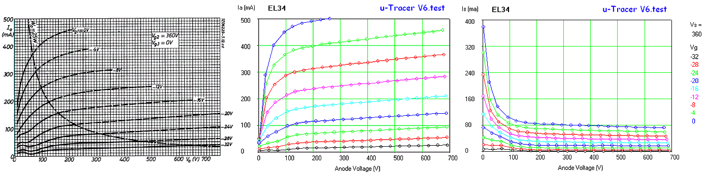
Figure 10.3 One of my favourite test subjects is the good old EL34 (6CA7), here compared to the graphs in the Philips datasheet. Care has been taken to measure the set of curves at exactly the same grid bias values as in the data sheet, and to plot the measurements on the same scale. For Vg up to -8 V, the currents are nearly the same as in the data sheet, at higher currents the tube seems to output even more current than in the data sheet. The right graph gives the screen currents which can be substantial for lower anode voltages.
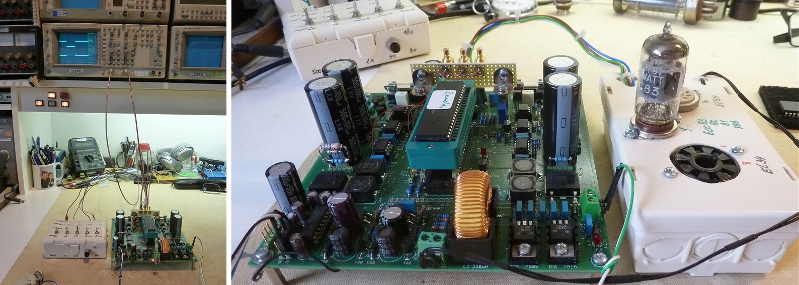
Figure 10.4 Few snapshots of the test setups that are used to evaluate the uTracer6. On the left side the resistor box and some pulse checking on the scope. The right picture shows the tube test box that is used for quick tube measurements and for repair jobs on defect uTracer3ĺs that people sometimes send me.
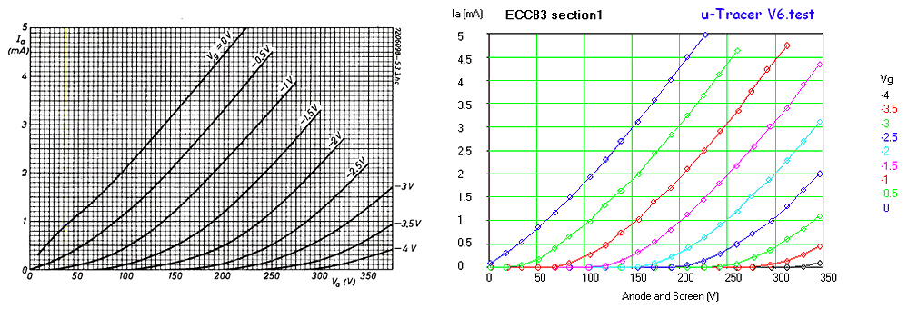
Figure 10.5 Despite the fact that the uTracer6 has been configured for the highest current range in this set of measurements, it also shows a very acceptable performance at lower currents as this measurement of an ECC83 (12AX7) shows.
Figure 10.6 Finally, one of the ultimate monsters in my collection, the PL519 (40KG6A) a power line output pentodes for colour televisions that was introduced in 1970 just before transistors made their entry in the line deflection unit of televisions. The measurements look a bit ônoisyö. This can have something to do with the improvised socket I used, or it can be inherent to the tube since it reproduced between measurements and three other PL519ĺs showed a similar behaviour, while the curves of the EUL34 above, measured in the same session produced perfectly smooth curves. The datasheet of the PL519 shows the curves up to 2 A! Well, that is perhaps something for a uTracer7 😉
With several uTracer6 boards built, it became time to test the board as thoroughly as possible before dispatching it into the hands of customers. So it was time to let somebody else play with it to get an independent impression on its functioning. For that I asked my colleague and friend Derk Reefman whom many of you will know from the SPICE tube models that he developed. Derk is an experienced uTracer3 user, and he is used to working with different tubes in other ways than I do.
Figure 11.1 An EL51 being tested by Derk Reefman (left) and output characteristics (right).
After an obligatory first resistor test - which indeed showed that the uTracer6 can go up to 1 kV - Derk tested an EL51 (Fig. 11.1). The EL51 is a powerful audio pentode that in class A can generate 67 Watts and in class B 140 Watts of audio power. With a typical anode bias voltage between 500 and 750 volts - depending on the mode of operation ľ it is beyond the reach of the uTracer3. The uTracer6 as well as the EL51 both operated as expected.
Oscillations
It may be recalled from the last instalment on this page that I had some strange results when I traced a PL519/40KG6A (Figure 10.6). At the time I attributed it to the dodgy magnoval socket that I rarely use. I didnĺt immediately think of oscillations since in the uTracer3 oscillations tend to manifest themselves as ôviolent dips and jerksö in the curves, and not as the type of ragged curves that I observed here. Triggered by my observations on the PL519, Derk decided to also test a PL509, which is almost identical to the PL519. To my surprise this also produced similar ragged curves. This now clearly pointed to a deeper and more serious problem, oscillations!
Oscillations are the nightmare of every tube tester/tracer user (and builder). They are a manifestation of one of my favorite versions of Murphyĺs Law: ôamplifiers always oscillate, and oscillators never start.ö Oscillations are an almost inherent problem of tube testers; you take a tube, connect it with too long wires that undoubtedly will have inductive and capacitive parasitics, and you bias the tube in its optimal bias point where it has maximum gain. It is almost a miracle when it doesnĺt oscillate! I remember from the time I made RF transistors at Philips that we were always fighting oscillations in our semiconductor curve tracers and parameter analyzers, and that was not due to a lack of inferior measurement equipment, so we are in good company.
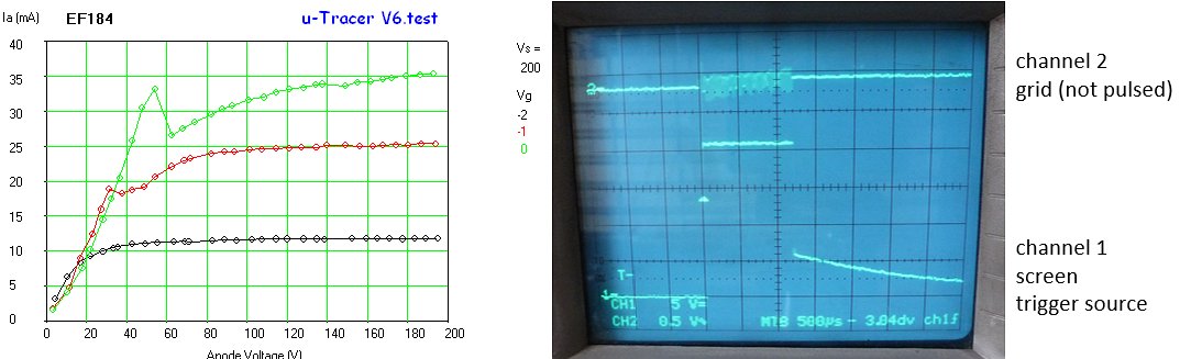
Figure 11.2 Oscillations in an EF184. To observe the oscillations a memory scope is needed. Connect one trace to the screen output and use that as a trigger, and connect the other trace to e.g. the grid connection.
Realizing that the PL509/PL519 are tubes with a very high transconductance (I measured values between 30 and 40 mA/V), and that high transconductance tubes are more prone to oscillations, Derk decided to test another high slope tube, the EF184(6EJ7). The EF184 is an IF tube with a transconductance of 15 mA/V, and an improved version of the legendary EF80. Surely enough, also this tube oscillated both in Derks uTracer6 setup, as well as in mine. A first observation therefore was that apparently the uTracer6 is more prone to oscillations than the uTracer3, since the EF184 never caused oscillations before. A second observation was that since some EF184 tubes consistently oscillate while others donĺt - despite the fact that they all tested identical on the uTracer3 - the cause for oscillations is not very clear and may depend on small details!
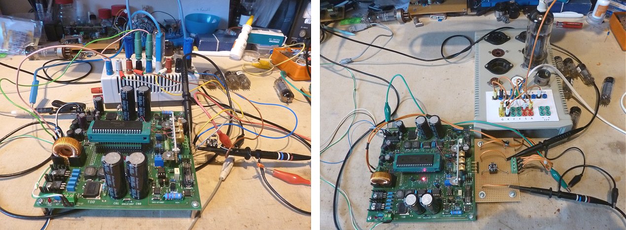
Figure 11.3 Changing the setup from the ôad-hocö arrangement on the left to the ôcorrectly wiredö arrangement using the socket array of my uTracer3 in my case already suppressed the oscillation in a number of EF184ĺs. Note that on the right a special board was inserted between the uTracer and the sockets to allow for easy experimenting with oscillation suppression ôtricksö.
Preventing oscillations
Since the origin of oscillations can be quite diverse and vary from tube to tube and construction to construction, it is impossible to give one specific remedy that will work on all cases. There are a number of ôtricksö that can be tried, individually or sometimes in combination, that are all aimed at reducing the gain of the tube at RF frequencies without affecting the DC behavior.
As general guidelines to prevent isolations I always advise people to: keep wires as short as possible, route wires in a loop around to all the sockets as invented and patented by AVO, and insert RFI ferrite beads over the wires at regular intervals (see also the construction manual). Should the oscillations nevertheless persist, then the following measures can be tried:
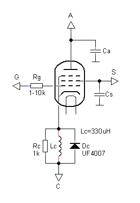
-- Grid stopper resistor
A simple resistor in series with the grid, a so called grid stopper, is a well-known trick to suppress spurious oscillations in tube amplifiers. Whereas in RF amplifiers usually a resistor value in the range of 50-100 ohms is chosen so as not to kill the gain at the desired frequency, in the uTracer a much higher resistance value in the range of 1 ľ 10 kohm can be used since the uTracer is operating at such a low frequency that it can be considered as DC.
-- Inductor//resistor in series with cathode
A method that proved very effective in suppressing oscillations in both the setup of Derk as well as mine was to include of a parallel combination of a 330uH inductor with a 1k resistor and a ôflybackö diode in series with the cathode lead (see figure to the right). At the low frequency at which the uTracer operates the inductor behaves as a short, while at high frequencies the inductor becomes an open with the resistor killing the RF gain of the tube. The snubber diode absorbs any transients that could occur should the current be suddenly interrupted. Feel free to experiment with the inductor and resistor values. All three components are supplied with the kit by the way.
-- Anode / Screen load capacitor
Sometimes adding a tiny capacitor to ground to either the anode and/or the screen can effectively suppress oscillations. In a particular setup I had an oscillating EL84 that stopped oscillating as soon as the anode was loaded by the tiny capacitance of an oscilloscope probe (10:1). Feel free to add capacitances up to several hundreds of pF, but mind their maximum working voltage.
-- Insert a lossy anode inductance
The standard way to suppress oscillations in RF tube circuits seems to be the insertion of a lossy inductor in series with the anode lead. For interesting articles read here or here. One of the beta testers obtained very good results with the insertion of a large RFI suppression bead in the anode lead (see Fig. 11.4).
As mentioned sometimes a combination of measures is required. In my case the very high slope PL519 could only be silenced through a combination of the cathode inductor network and a 4k7 grid stopper.
Figure 11.4 The large RFI suppression bead successfully used by one of the beta testers to suppress oscillations in high power tubes.
Low current mods
In the previous section on this page it was explained how the selection of the current sense resistors is a compromise between maximum current range and noise performance at low currents. Depending on the type of tubes you plan to test, a more optimal choice for the current sense resistor may be possible. In one of the development versions of the uTracer6 I used a simple jumper to switch between two current ranges (Fig. 11.5). I used a permanent resistor of 18 ohm which, just as for the uTracer3, results in a current range of 200 mA. By inserting the jumper two additional 10 ohm resistors are connected in parallel to the 18 ohm resistors resulting in 18//10//10 = 3.91 ohm, corresponding to a maximum current range of about 920 mA.
Some of you might want to consider making the current range selectable with a switch on the front panel. I did not try this myself, but for those of you who are considering this option I have the following recommendations:
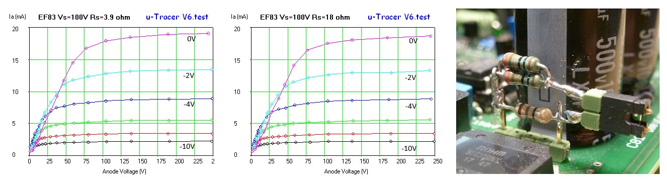
Figure 11.5 An EF83 traced with a 3.91 ohm current sense resistor (left) and with a 18 ohm current sense resistor (middle). In my test setup I use a simple jumper to switch between the two (right).
Figure 11.6 An EF40 traced with a 3.91 ohm current sense resistor (left) and with a 18 ohm current sense resistor (right).
The curves for an EF83 and an EF40, both traced with a 3.9 ohm current sense resistor and an 18 ohm sense resistor (Figs. 11.5 and 11.6) show that even with the 3.9 ohm resistor the low current behavior is quite acceptable and that the 18 ohm resistor only shows a marginal improvement. During the development of the uTracer6 I mostly tested the circuit using fixed resistors connected to the anode and screen channels (See Fig 10.2) and there I could observe a distinct improvement. I guess that with a real set of curves the eye is less sensitive to somewhat more noisy curves than for a straight line.
Shorts and wiring mistakes
Anode/screen to cathode/grid shorts
Although both the uTracer3 as well as the uTracer6 have been designed to withstand full short circuit conditions (anode and/or screen connected to cathode or grid), experience has shown that sometimes the protection circuit does not hold, resulting in the destruction of the high voltage switch transistor. Although this is not an enormous disaster - the transistor is less than a euro and is replaced in a minute or so - it never happens at a convenient moment. In the uTracer6 there is an additional safety feature that protects the output stage for a wiring error, or a tube with a short. When either the anode or the screen output are directly connected to the cathode or the grid, it will cause the respective fuse to blow. The reason is that immediately before a measurement pulse the HV switch buffer capacitor C65 is charged through T61 and D64 (Fig. 11.7A). When the output is connected to the cathode (which is a Vsupl = 19.5 V) this will immediately blow the fuse. If for any reason this feature is not desired, a 47 ohm resistor placed in series with D64 will limit the current saving the fuse, while it will still charge C65 fast enough.
Grid to Cathode shorts
The LTC6090 which provides the grid bias appears to be quite sensitive for direct shorts of the output to the positive supply rail (the cathode). To prevent damage to the LTC6090 in case the grid output is accidentally shorted to the cathode, I recommend to have always jumper J2 installed during normal operation (pulsed grid), and to standard insert a 10k current limiting resistor in series with the grid (Fig. 11.7B). Since the grid current in normal operation is practically zero, this has no effect on the measurement and has the additional benefit that it will help suppressing oscillations. Only for grid bias values very close to zero (-0.2 to 0V) there will be small voltage drop.
A practical configuration is the circuit shown in Fig. 11.7B. In normal operation switches Sc and Sg are open to suppress oscillations and protect the grid bias circuit. Sc can be closed for high current measurements where the cathode current might otherwise cause a voltage drop over the DC resistance (< 0.5 ohm) of the inductor. When measurments very close to Vg=0V are carrier out, and when the user is assured of the fact that the grid is properly connected and that there is no internal grid/cathode short in the tube, Sg can be closed to bypass the grid protection resistor.
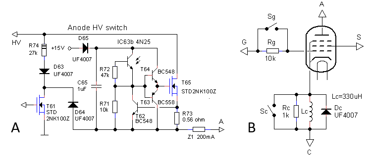
Figure 11.7 Anode/screen section (left) and proposed tube connections (right).
How about the 6146B?
Readers of this page will remember that in the introduction I stated that one of my goals for the uTracer6 was to be able to trace the popular ham radio transmitter tube 6146B. In transmitter circuits this tube is driven by both positive as well as negative grid voltages. The positive grid voltage characterization obviously will have to wait until the extension board is ready, however, the characterization at negative grid voltages is peanuts for the uTracer6 (Fig. 11.8)!
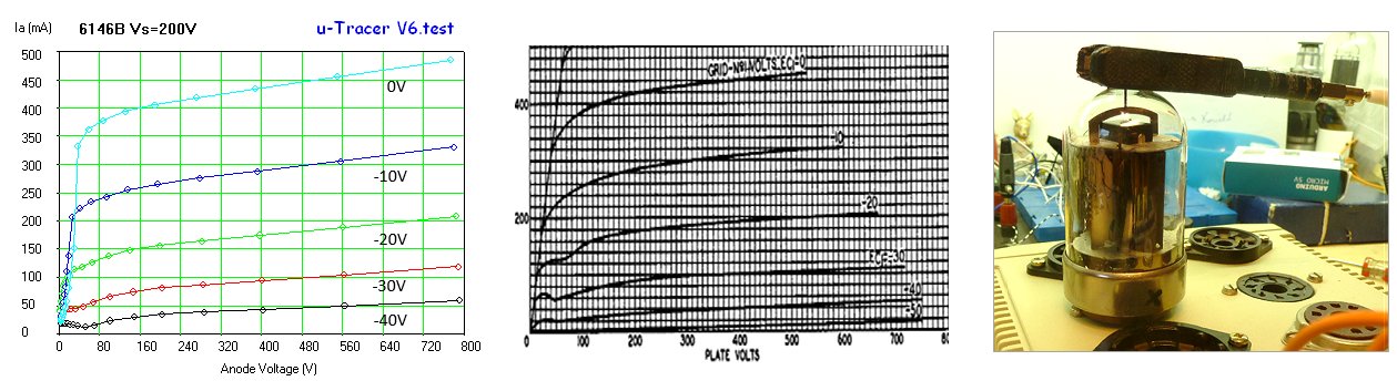
Figure 11.8 The 6146B traced for negative grid voltages with the uTracer6. Note that the datasheet graph has been stretched to the same scale as the uTracer graph.
The uTracer6 kit!
The uTracer3 was never meant to be a kit. It started out as just a project for myself. However, when people read about it in my blog, many liked the concept and asked if I could turn it into a kit. I wasnĺt immediately enthusiastic about the idea. I have quite a busy job and the idea of dealing with customers and the problems they inevitably would encounter didnĺt really appeal to me. However, my sons, at that time aged around 14 persuaded me to do it and I never regretted it! Dea ling with so many enthusiasts all around the world has been really rewarding both for myself as well as for my wife who is taking care of the financial and logistic side of ôthe business.ö
We started with ten uTracer kits in the hope that we would ever earn back the investment. In my wildest dreams I imagined that perhaps one day we could sell about fifty of them. I could never have imagined that now at the time of writing of this page we would have sold more than 1650 of them in 56 countries! It has been a tremendous success.
Over the years I received, many request for a uTracer that could handle higher voltages and higher currents. After a few studies that didnĺt end in anything that could be sold as a kit, I am quite proud that this has now resulted in the uTracer6 which I think nicely balances on the thin line between complexity and performance.
We started the uTracer3 adventure without any notion of what it means to sell a product, especially not to sell 1650 of them. From time to time small mistakes or problems were identified that sometimes took a lot of time and effort to solve by communicating them to people, shipping replacement components etc. So no wonder that the experience with the uTracer3 has made us a bit more cautious. For this reason, I first asked Derk to play with the new uTracer6. A good decision, since in this way we discovered that the uTracer6 is more prone to oscillations than the uTracer3 and fortunately we found ways to mitigate the problem. Next, from the list of people who have already experience with the uTracer3, and who have indicated to us that they are also interested in buying a uTracer6, we selected ten ôbeta testersö who are now building and testing the uTracer6 with the goal to come to a product that is as ôfool proofö and reliable as the uTracer3.

Figure 11.9 With continuous temperatures in excess of 38C, the week of 8-15th of August 2020 was the hottest period ever recorded in Holland.
Despite the heat, Marie-JosÚ caught me extremely happy to complete the first set of ten uTracer6 kits (left)!
Our ôÚminance griseö Riva, a retired guide dog who is enjoying her pension in our family, does not seem impressed by the first batch of six uTracer6 kits to be shipped to beta testers all over the world (right).
The past months ten ôbeta testersö around the world have constructed the uTracer6 and used it to test a variety of tubes. Overall the experiences have been positive, but a number is issues emerged that will be discussed below.
Construction
In general the construction went quite smoothly and all beta testers praised the clarity of the manual and the step-by-step approach of the construction. A few small issues emerged:
öBumpsö
Several beta testers observed small bumps or sometimes dips in the anode current for anode and screen voltages around 180 V. A complication was that with the two uTracer6 boards that I have these bumps could not be observed, even using the same settings and same test subject, which made it difficult for me to work on the problem. It took some going back and forth to identify the source of the problem that appeared to be related to the ôintelligent chargingö algorithm discussed in section 9 of this page (click here). To increase the accuracy at lower anode and screen voltages, this algorithm increases the width of the boost converter charge pulse from 10 us to 40 us when either the anode or the screen voltage is above a certain threshold value. For the beta uTracer6 this threshold was set at 180 V. Admittedly, the 40 us boost pulse is on the edge of driving the inductors in the boost converters into saturation. Depending on small variations in the inductors and the supply voltage, apparently in some cases the inductors were indeed driven into saturation resulting in a sharp increase in current consumption which probably caused small variations in the screen voltage resulting in the bumps in the anode current. The problem has been solved by the introduction of a new algorithm that gradually increases the boost converter charge pulse width when the voltage increases.
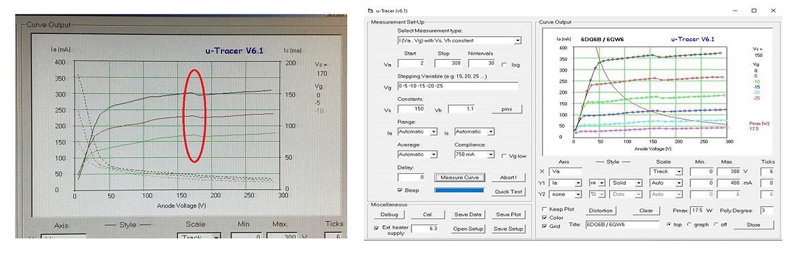
Figure 12-1 Examples of kinks and bumps in the anode current of pentodes reported to me by beta testers. The problem has been solved with a smoother boost converter charge algorithm.
Oscillations
As already signaled in the previous section, the uTracer6 appears to be more susceptible to oscillations than the uTracer3. The occurrence of oscillations depends heavily on the wiring of the uTracer to the tube sockets. Some builds hardly show a tendency to oscillate, while for other constructions it is very difficult to stop oscillations. There has been quite extensive back and forth communication with the beta testers about this issue, which has resulted in a list of measures that can be implemented to stop the oscillations. Unfortunately, there appears to be no definite solution that works for all tubes in all builds, so some individualized tweaking may be required. Whereas the uTracer3 has proven to be a more or less fool proof, plug and play tube tester/tracer, the uTracer6 requires a bit more attention to coax it into proper operation over its wide bias range.
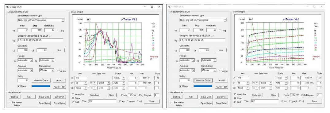
Figure 12-2 Left: an 807 tube of one of the beta testers heavily oscillating. Right: same tube silenced after some tweaking with gridstopper/snubber circuits.
The grid supply
It appeared that, again under some load conditions, the grid bias circuit was oscillating. So not the tube, but the uTracer6 circuit itself. The problem was readily solved by adding a small capacitor in parallel to the feedback resistor of the high voltage OpAmp LT6090. Obviously this modification has been included into the final uTracer6 PCB.
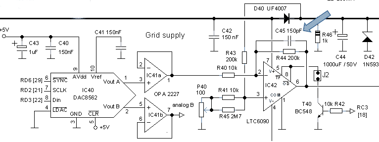
Figure 12-3 A small 150 pF capacitor prevents the LT6090 high-voltage OpAmp from oscillating under all conditions.
Triode curves not fully drawn
One beta tester noticed that in some cases, especially for ôheavyö triodes, the curves are not fully drawn (see example Fig. 12-4). Why is that?
It is quite a long story and the reason is closely related to the working principle of the uTracer (3 and 6). To explain it let me re-cap how the uTracer works. The uTracer charges a big cap to a pre-defined voltage,e and then connects this cap to the tube under test during 1 ms (measurement pulse). At the end of this 1 ms interval it measures the actual currents and voltages. It is important to realize that this voltage will be lower than the set point because during the 1 ms measurement pulse the cap will have discharged somewhat depending on the current drawn.
At the same time one of the safety measures in place is the current compliance. When the maximum current is exceeded at any given moment during the measurement pulse, the tube is immediately switched off and the measurement point is not drawn in the graph.
So what happens, particularly with triodes, is that for higher currents the Ia(Va) curves becomes very steep. Now, when the next point is measured, and that point exceeds the maximum current, the measurement is interrupted immediately and the curve ends at the last point measured! Note that due to the discharging the voltage of this point is lower than what would be expected! One way to mitigate the ôproblemö is to increase the number of measurement points. Some people find it difficult to understand that although the plotted voltage values are lower than the set-point voltages the curves are still accurate. The answer is that since although plotted voltage values deviate from the set point values, the drawn curve is still accurate since the voltage-current pairs are measured simultaneously.
Personally, I donĺt think the fact that the curves are not fully plotted is a very big deal. The parts of the curves not drawn contain hardly any additional information and can simple be extrapolated from the part of the curves that is plotted at lower currents. However, with a bit of effort and trickery it is possible to complement the curves if absolutely needed:
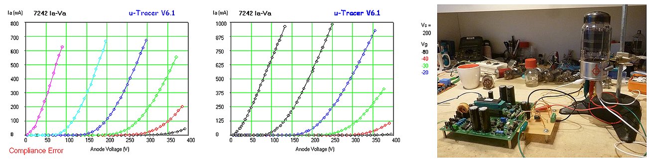
Figure 12-4 The 7242 (right) is a beast of a triode - the heater alone draws 7A at 6.3V - that nicely illustrates how curves are not completely drawn to the compliance limit (left). With a little bit of tweaking, however, the full curve can be obtained of needed (middle).
| Characteristic: |
|
|
|---|---|---|
| Anode and screen supplies |
|
|
| Grid supply | Voltage range: -50 V to 0 V |
Voltage range: -100 V to 0 V (standard uTracer6) An extension board (grid shield) is in preparation that will extend the grid bias range to positive grid biases 0 V to +100 V, including grid current measurement 0 ľ 100 mA. |
| Internal heater supply |
Voltage range 0 ľ 19.5 V (max. 1.5A) Much has been written about the heater supply of the uTracer3. The heater supply PWM modulates the supply voltage at a frequency of 19.5 kHz. Due to this relatively high PWM frequency parasitic inductances in the leads will result in a lower effective heater voltage, especially for lower heater voltages. For this reason, many users prefer to use an external heater supply. |
Voltage range 0 ľ 19.5 V (max. 1.5A) Compared to the uTracer3 the PWM frequency has been reduced to 1.2 kHz. This makes the effective heater voltage virtually insensitive to parasitic wiring inductances, resulting in more accurate heater voltages. |
| Maturity | With more than 1700 uTracer3 units in operation in over 55 countries, the uTracer3 kit by now has been well debugged and has proven itself in the field. If problems during construction occur, they can usually be solved by email. In incidental cases it is necessary to return the PCB to me for debugging, but in the end they all work as expected. | So far about 10 ôBeta testersö have constructed the uTracer without significant problems. With their feedback the PCB and the construction manual have been updated. However, obviously the uTracer6 still has to fully prove itself ôin the field.ö |
| Oscillations |
Oscillations is a problem inherent to tube testers and tracers. The combination of a tube biased in its optimal bias point in combination with long wires and unpredictable parasitics are almost an invitation for the tube to oscillate. Oscillations sporadically occur in the uTracer3. Fortunately, it is often quite simple to suppress these oscillations by means of careful routing of the wires to the tube sockets and/or by implementing a grid stopper resistor.
Read more here. | Compared to the uTracer3, the uTracer6 is more susceptible to oscillations, and when they occur these oscillations are more difficult to suppress. The occurrence of oscillations heavily depends on the wiring to the tubes. Some uTracer6 builds show no tendency to oscillate at all, while others are very difficult to ôsilence.ö A variety of measures to stop oscillations has been collected, but nevertheless silencing a particular tube requires some tweaking and ôfingerspitzengefuhl.ö This makes the uTracer6 more an instrument for experienced users. |
| Application range | The uTracer3 is in my opinion the ideal tester / tracer for 90% of all tubes. It is well debugged, relatively forgiving with respect to oscillations, and it will practically cover all common radio, television and amplifier tubes. Despite the fact that some tubes are specked to, or used at voltages higher than 400 V, most important tube parameters can be determined at voltages well below 400 V. | Especially because of the higher susceptibility to oscillations the uTracer6 really is the tester for the more experienced user who really needs the extended voltage and/or current ranges, or the future possibility of positive grid voltages (in combination with the possibility to measure grid currents). Especially ham radio enthusiasts will appreciate the extended capabilities of the uTracer6. |
| Robustness | With more than 1700 uTracer3 units in the field, the uTracer3 has proven itself to be quite robust against misuse, shorts etc. Worst-case three low cost transistors in the high voltage switch need to be replaced to return the uTracer3 back into operation. The cases that this is needed are so relatively rare that I am happy to provide these components for free if needed. | With the uTracer6 there is obviously less experience with respect to robustness. In contrast to the uTracer3 a measure has been implemented whereby a hard short will blow out a fuse preventing damage to the semiconductor components. To protect the grid supply against hard shorts it is recommended to always use a 4k7 resistor in series with the grid supply and always have jumper J2 (pulsed grid operation) in place. |
| Availability: | The uTracer3 kit is assembled in batches of 25 pieces. We try to have a number of kits available at any time, however, small delays of a few weeks can occur when sales temporarily outrun the assembly of a new series of kits. | To gain experience with the uTracer6 we decided to limit the first series of uTracer6 kits to 50 pieces after which we will take some time to evaluate the uTracer6. For this first series of 50 uTracer6 kits shipment will be limited to those countries where a swift delivery is guaranteed. These include: countries of the European Union (please contact us for countries boarding to the EU, e.g. UK, Norway etc.), USA, Australia, Japan. |
| Price: |
Prices include shipment worldwide and assistance with construction including mail support and physical debugging of the unit if needed in incidental cases. Prices include: PCB with SMD components assembled, all other components (ôdifficult to identify components in labeled bags), and a printed and bounded manual. Not included are: USB to serial cable, 19.5 supply (old laptop power supply), tube sockets etc. |
Prices include shipment worldwide and assistance with construction including mail support and physical debugging of the unit if needed in incidental cases. Prices include: PCB with SMD components assembled, all other components (ôdifficult to identify components in labeled bags), and a printed and bounded manual. Not included are: USB to serial cable, 19.5 supply (old laptop power supply), tube sockets etc. |
With the first series of uTracer6 kits now being shipped to enthusiasts all around the world, it has become time to start thinking about the positive grid bias extension board. First of all, why an extension board and why didnĺt I just include the positive grid supply on the uTracer board itself? The reason is simple, most people will never need a positive grid bias so why then pay for this option, not only with additional components, but also extra board space? On top of that, all these extra features would have delayed the development of the uTracer6 significantly. An extension board seemed to me the best solution to make this additional feature available for those who need it. In this section some first thoughts about the extension board circuit.
Circuit overview
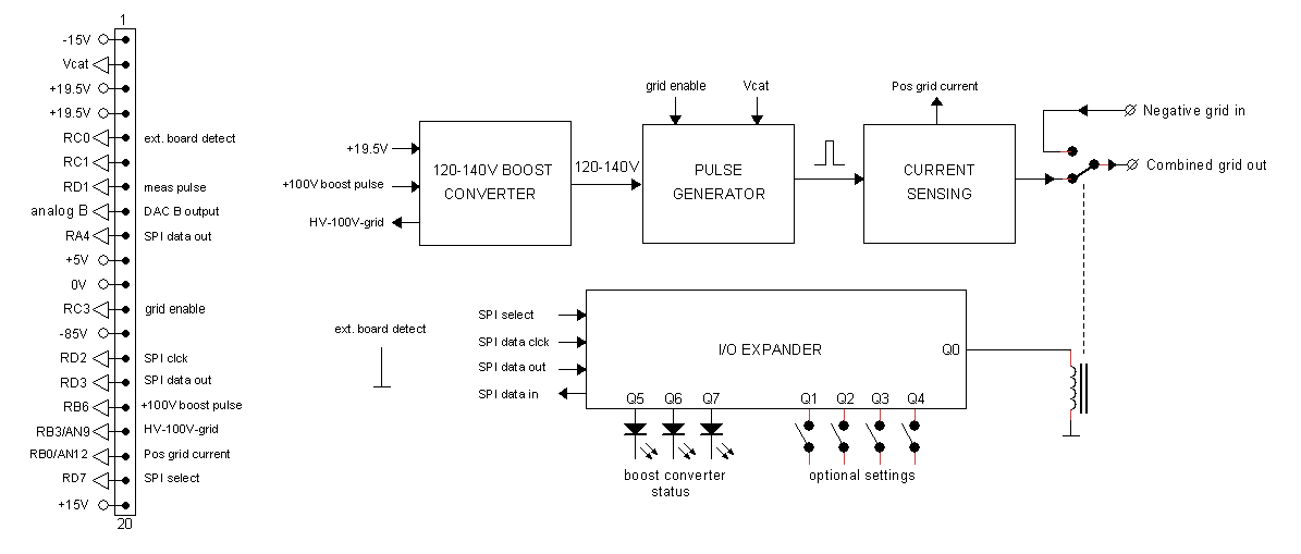
Figure 13.1 Preliminary block diagram of the positive grid bias extension board.
Figure 13.1 shows the block diagram of the extension board as I have it in mind at this moment. Input RC0 of the PIC is on the uTracer board pulled up by a 10k resistor. On the extension board RC0 is tied to ground. In this way the presence of the extension board can be detected. The idea is that at reset the processor polls the RC0 input and based on the level of the pin starts up in ôconventionalö mode or in the ôextensionö mode.
Since positive grid biases will result in a grid current, the grid bias is - just as the anode and screen voltages - not applied continuously, but pulsed. A first idea could be to implement the grid bias circuit in exactly the same way as the anode and screen bias circuits. However, a grid bias circuit requires more precise control than the anode and screen biases, especially at lower values! I therefore have the idea to implement the grid bias section in a rather conventional fashion in a circuit consisting of a high voltage supply, a programmable pulse generator and a ôhigh-sideö current sense circuit.
The supply voltage for the positive grid bias circuit is generated by yet another boost converter - the fifth now in total - that is controlled by the PIC on the uTracer board. The boost converter requires two control lines. One for the boost pulses generated by the PIC and one for a feedback line that is used by the PIC to monitor the output voltage. For the moment the target output voltage is 120 to 140V.
The next circuit block is the grid pulse generator. A complication is that the pulse is referenced to the cathode and not to ground. So one of the control lines for this block is obviously the cathode potential. Another input is the 0 to 5V voltage from the second DAC on the uTracer board. The circuit has to map the 0-5 voltage range to the 0 to +100V grid bias output referenced to the cathode potential. Finally, the block uses the grid enable signal that turns the grid pulse on and off before and after the measurement pulse itself. The circuit should be able to supply a grid current up to 100 mA.
The last block measures the grid current. This is far from trivial! The elegant trick that is used in the uTracer to measure the anode and screen currents at first sight could not be used here, so the current really has to be measured high side. Later on we will see that that turned out to be more difficult than expected. More on this later on. The current sense circuit uses analog input AN12 of the PIC.
The idea is to do the selection between the negative grid bias supply on the main board and the positive grid supply on the extension board by means of a miniature relay that is controlled by the PIC. I plan to use an SPI I/O expander to have a number of additional digital I/Oĺs on the extension board. The expander can drive the relay, but also a few status LEDs that indicate if the boost converts are functioning as they should, while it is also possible to set some options by means of jumpers.
The pulse generator, a first not so good idea ů
The heart of the circuit is obviously the pulse generator circuit. Its primary function is to translate the 0-5V signal from the positive grid bias DAC (DAC B), which is referenced to ground, to a pulsed output signal ranging from 0 to +100V that is referenced to the cathode potential.
Figure 13.2 The first idea for the positive grid bias circuit uses a simple summing amplifier circuit.
A first thought was the circuit depicted in Fig. 13.2. The circuit around OpAmp A1 is a simple summing amplifier. Its output is the sum of the two input signals Vcat and Vdac that are weighted by resister ratios R3/R1 and R3/R2 respectively. Note that Vdac is amplified by a factor of -2 while Vcat is attenuated by a factor of -10! The high voltage OpAmp A2 amplifies the output signal of A1 by a factor -10 so that at the output of A2 we find the desired grid bias Vcat + 20Vadc. Pulsing of the output can be simply done by enabling the output of the OpAmp similarly to the pulsed negative grid bias supply.
At first I was quite pleased with this simple and transparent solution until I started to make some calculations to estimate the worst case offset of the circuit as a result of the offsets of the OpAmps and resistor value tolerances. Normally I tend to think that using 1% resistors is sufficient to have most circuits run perfectly, however, a simple analysis shows that even using 1% resistors can cause significant errors even in circuits as simple as this one.
Of course this is a worst case analysis. In reality the offset will be (much) smaller since it is unlikely that all resistors will have their maximum deviation in exactly the worst direction! Toiling with the circuit I intuitively felt that it would be better to reference A2 to Vcat instead to ground so ů
The pulse generator, a second (slightly better) idea ů
Figure 13.3 Second attempt for the pulse generator circuit.
Figure 13.3 shows the second circuit idea where A2 is referenced to ground. OpAmp A1 now is configured as a subtraction circuit. The circuit diagram is pretty straightforward and the equations in Fig. 13.3 explain what is going on. To study the effect of component tolerations we write the output voltage of A1 as:

To minimize the offset, the output voltage of A1 should be exactly equal to Vcat when Vdac is zero. To achieve this the term (R4/(R2+R4))*((R1+R3)/R1) should be exactly equal to unity. Obviously all four resistors R1, R2, R3 and R4 can deviate +/- 1%. For me it was not a priori clear which combination gives the largest total deviation. I am pretty sure there must be more intelligent ways to do this, but nevertheless I did a little exercise where I looked at all possible combinations:
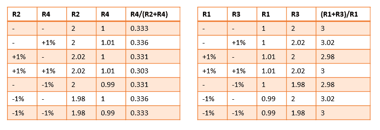
Figure 13.4 Calculation of the effect to resistor tolrances.
From this we can calculate the maximum offset as a result of resistor tolerances:
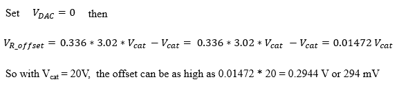
So a bit better than the previous circuit, and in reality most likely much better than this worst case calculation, but despite this the circuit will nevertheless need some means to manually compensate for the offset by means of a trimmer.
The pulse generator, third time lucky?
This is, for the time being, the last circuit idea in this series. The disappointment of the last circuit left me with the feeling that there simply had to be a circuit solution that would do the job without the need for manual offset correction. I think it took a couple of drinks for me to realize that a simple current source can do the trick! Near ideal current sources can easily be realized and the current they supply (or sink) is independent of the voltage so that they are ideal for level shifting!
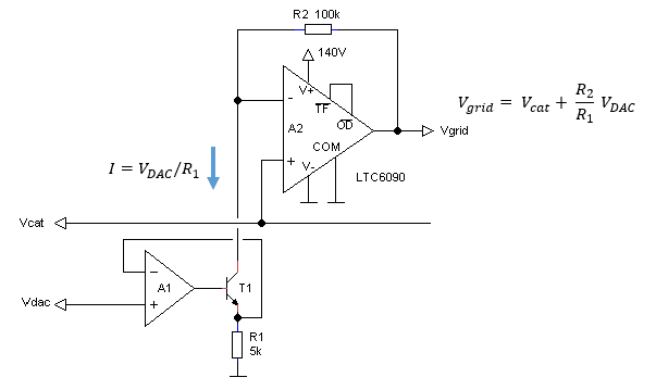
Figure 13.5 This last circuit uses a current source to level shift the DAC voltage.
Figure 13.5 shows the basic circuit. The circuit around OpAmp A1 is a simple voltage to current converter. The OpAmp adjusts the current through the transistor so that the voltage over R1 is exactly equal to the input voltage. If we neglect the base current of the transistor, then the current sinked by the transistor is exactly equal to Vdac/R1. This current has to be supplied by OpAmp A2 through resistor R2 whereby the OpAmp will adjust the output voltage in such a way that the voltage on the negative input equals the voltage on the positive input: Vcat. So it is not difficult to see that Vgrid = Vcat + (R2/R1)Vdac.
So how about offsets? It is important to note that tolerances of the two resistors values does not result in offsets, but just in a variation in gain, which can easily be compensated for in software during the calibration. That leaves us with the offsets of the OpAmps.
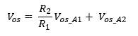
The offset introduced by A2 is at most equal to the intrinsic offset of the OpAmp A2 since there is no voltage gain involved. According to the datasheet this is typically 0.33 mV and at most 1.25 mV. The offset of OpAmp A1, an
LTC6090,
is amplified by a factor (R2/R1). For A1 I plan to use a modern
OPA202
OpAmp. This modern precision 36 V OpAmp has a typical offset voltage of 20 uV (!) and a maximum offset voltage of 200 uV. Using the equation above and assuming a gain of 20, we arrive at a typical offset voltage of 0.73 mV and a maximum offset of 5.25 mV. I am sure that everybody can live with that!
Towards a complete circuit
After these deliberations, it has become time to come to a first experimental circuit. starting point for this circuit were the following specifications:
As mentioned, measuring a high side current in high voltage circuits is always a bit of a problem. In first instance my eye had fallen on an very nice IC from analog devices, the LT1990. This differential amplifier has a very high common mode input voltage range of +/- 250V, and appeared to very suitable for measuring high side the current supplied by the positive grid supply. Unfortunately, I never got this circuit to work as it should. I am not going to bother the readers here with every failed circuits, but for prosperity the circuit diagram of this circuit can be found here. Problem with the LT1990 was that I didnĺt manage to get it to operate without a considerable offset current. I spend several days debugging the circuit, but never found the cause. After blowing up several LT1990 chips, which by the way are quite expensive, I decided to abandon the whole plan and return to the proven concept also used in the anode and screen supplies of the uTracer3+.
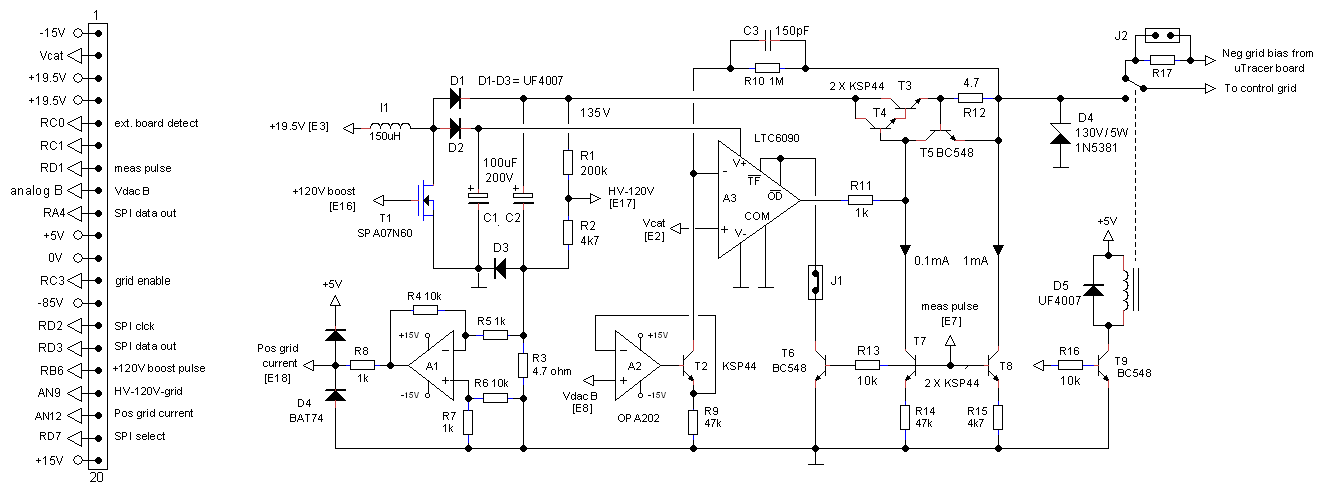
Figure 13.6 First experimental version of the positive grid bias circuit.
Figure 13.6 shows the circuit diagram of the first concept of the positive grid bias circuit I arrived at. As mentioned, the circuits is based on the same current sensing principle as the anode and screen supplies. Interested readers can find more information on the basic principle here. At first sight the circuit looks rather complex, but fortunately it can be broken down in a number of simple sub-circuits.
The circuit around T1, C1 and C2 in the upper left corner is the high voltage supply boost converter. People familiar with the anode and screen boost converters of the uTracer will recognize in T1, D2 and C1 the topology of the basic boost converter circuit. A little bit surprising is the second boost converter circuit consisting of D1 and C2 that is placed in parallel to the first boost converter (we will come back to why we need two boost converters later). A special feature, or if you like trick, of this circuit is that C1 and C2 will always be charged to exactly the same voltage. To understand this, assume for instance that the voltages of C1 and C2 are not equal. Now when T1 closes after L1 has been charged, the voltage over L1 will increase to the point that the diode connected to the capacitor with the lowest voltage will open so that all charge is dumped into that capacitor. This process continues until both capacitors have the same voltage. As in the anode and screen boost converters, the circuit is controlled by the PIC whereby the output voltage is sensed by one of the AD inputs of the PIC controller that is connected to C2 via a voltage divider R1 and R2.
We now arrive at the heart of the circuit which is the high voltage OpAmp A3 in combination with the voltage controlled current source around OpAmp A2. After the extensive considerations in the first parts of this write-up, the workings of this circuit needs no further expanation. There are however two additions to the circuit. In the first place a buffer stage has been added consisting of the Darlington pair T3 and T4. Note that the feedback resistor R10 of OpAmp A3 is connected to the output of the buffer stage instead of the output of A3 so that the voltage drop over T3 and R12 is compensated for. Transistor T5 is a protection circuit that limits the output current to approximately 150 mA.
A second modification is that A3 is not switched on continuously, but like the LTC6090 on the main board of the utracer6 is used in pulsed mode operation. The measurement pulse signal is an active low pulse generated by the PIC that is pulled low a fraction of a millisecond before the actual measurement pulse, and that is returned to a high level a fraction of a millisecond after the actual measurement pulse. So during the measurement pulse, T6 is switched off so that OpAmp A3 is switched on. After the actual measurement pulse it is important that the grid voltage return to zero as quickly as possible. This is taken care off by the two current sources around T7 and T8. Note that during the actual measurement pulse these current sources are switched off!
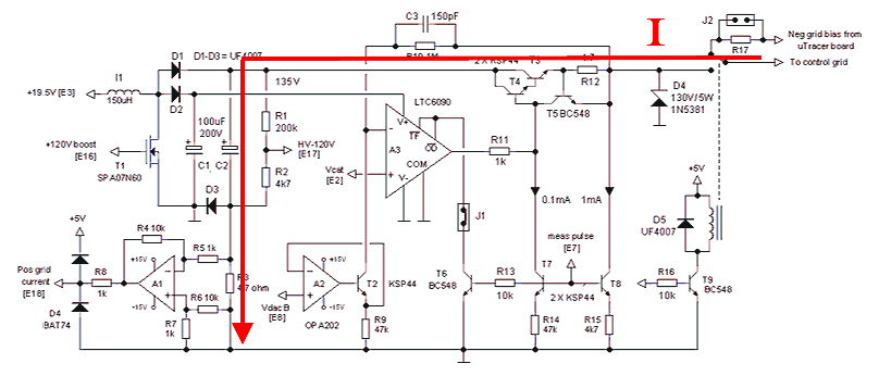
We finally arrive at the current sensing circuit itself, which is the circuit around A1. During the actual measurement pulse the grid current will have to flow through resistor R3 (see also the circuit diagram on the right). This current causes a negative voltage drop over R3 that is amplified by a factor of -10 by A1. The output signal of A1 is directly proportional to the grid current in the sense that Vout = 47*Igrid, so that 100 mA grid current corresponds to 4.7 V ADC input, almost the maximum range.
All this only holds when all the grid current is flowing though R3! To ensure this a number of measures has been taken. First of all, this is the reason why the high voltage supply has been split. By feeding A3 from a separate high voltage supply, the supply current of A3 is isolated from the grid current. It is also the reason why the current sources around T7 and T8 are switched off during the actual measurement pulse. It is impossible to prevent a small current leakage through R10. However, this current is very small (at max 100 uA at Vgrid = 100 V) and it can be compensated for in software because the leackage current is exactly (Vgrid ľ Vcat)/R10. Finally, by using the Darlington pair T3/T4 for the output buffer, the base current into this stage has been minimized.
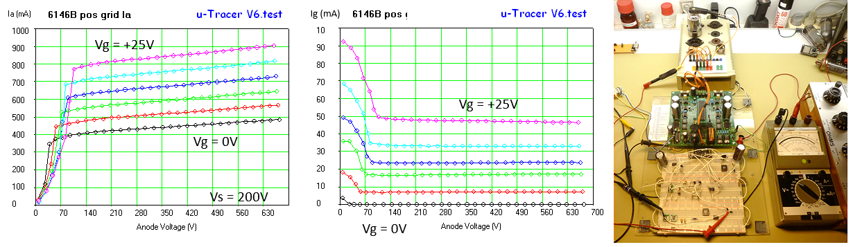
Figure 13-7 First measurements with the positive grid bias module on a 6146B for grid biases 0 to +25 V in 5 V increments.
First results were that the circuit worked like a dream. There is a lot more to tell about the circuit, but this section has already become way too long. Figure 13-7 shows one of the first positive grid measurements on a 6146B. In a next write-up I plan to show more examples and continue the discussion on the circuit and especially also the software.
After a turbulent year (COVID, component shortage and the introduction of the uTracer6), the positive grid extension board, including the necessary software changes, is now nearing its completion. Because this is always a very busy time of the year, it is difficult to find the time for a complete write-up, but I know that many people curious are interested how this little side-project is going on, so therefore here some lines with the key characteristics and a few pictures including some first measurements.
Main features:
The final hardware
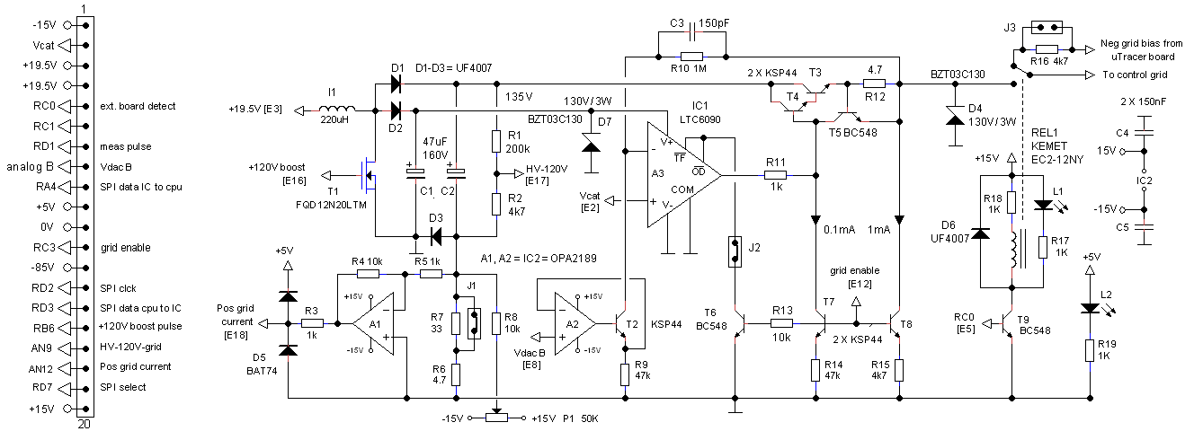
Figure 14-1 The final schematic of the positive grid extension board
Figure 14-1 shows the circuit diagram of the positive grid extension board that was used for the first series of 50 boards. Compared to the description of the circuit in the previous section, three small circuit modifications, and only some component selections changes were made. First potentiometer P1 was added to be able to adjust for some small offsets. Secondly, with jumper J1 the user has the possibility to select between two current ranges. With jumper J1 placed the current sense resistor is 4.7 ohm for a current range of 0 ľ 100 mA. With jumper J1 removed the current sense resistor is 33 + 4.7 = 37.7 ohm for a current range of 0 ľ 10 mA. Obviously, the correct value must be entered into the GUI.
Finally, a rather dirty trick is used to use I/O pin RC0 with as an input to detect the presence of the board, and as an output to control relays REL1. Remember that on the main board RC0 is pulled high by a 10k resistor. When the extension board is used, the emitter-base diode pulls the voltage on RC0 down to 0.8 V which is a logical zero. The trick used to control the relays is to make RC0 an input when the relays needs to be activated, and to make RC0 a low-output and the relays is not activated. A rather nifty trick that freeĺs up an I/O pin.
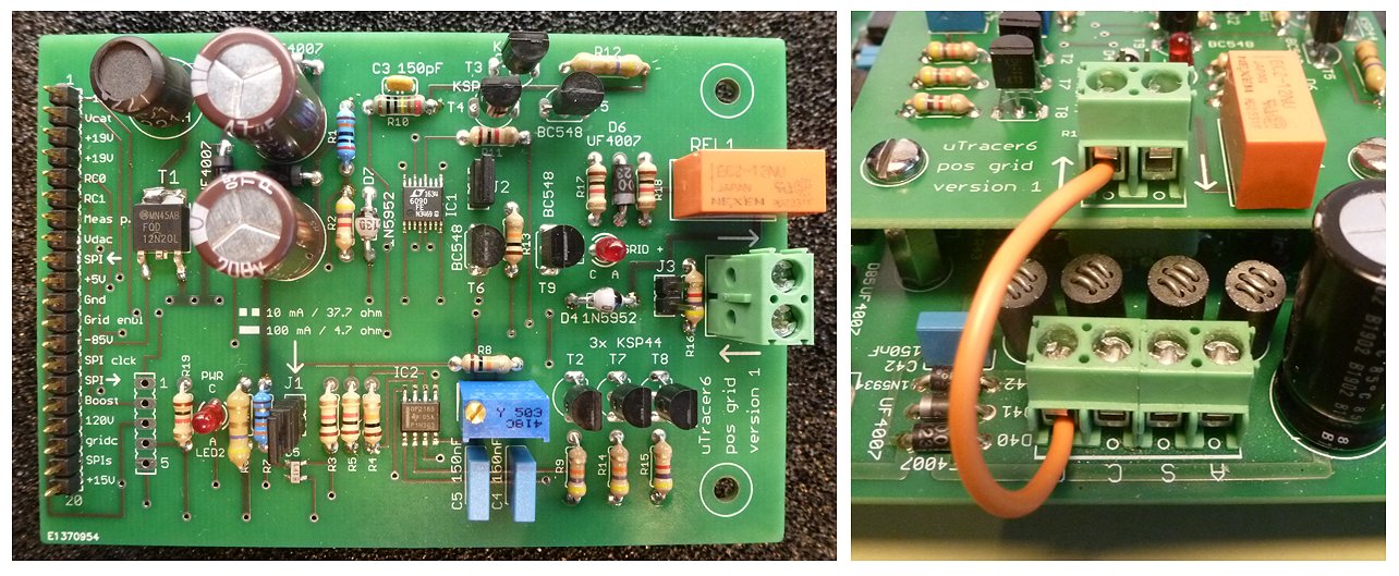
Figure 14-2 The completely populated extension board and how the grid input of the board is connected to the grid output of the main board. The grid output of the extension board is now the new grid terminal. Note that there is a provision yet another pin header which is for a small idea I have in mind.
|
|
Description: |
|---|---|
|
| This jumper is used to select the current range. It can be used to improve the resolution for smaller currents. With jumper J1 placed the current sense resistor is 4.7 ohm for a current range of 0 ľ 100 mA. With jumper J1 removed the current sense resistor is 33 + 4.7 = 37.7 ohm for a current range of 0 ľ 10 mA. Note the correct resistor values need to be entered into the appropriate field in the calibration form. |
|
| With jumper J2 place the positive grid supply is operated in its normal pulsed mode. When the jumper is removed, the output is continuous. The continuous mode is only used during calibration! In normal use J2 is always placed! Operating the positive grid supply in continuous mode can burn the grid of your tube! |
|
| Removing J3 will connect a 4k7 resistor in series with the negative grid supply. It can be used to suppress oscillations if needed. Normally J3 should be placed. |
Firmware and GUI modifications
The setting of the positive grid voltage was already incorporated in GUI version 6.1 and in firmware version 6.19 that was supplied in the first series of 150 uTracer6 kits. Click herefor a description of the communication protocol.
For the readout of the current, however, more extensive modifications to both the firmware as well as the GUI were necessary. The objective was to integrate the grids current in such a way that the new software is backwards compatible with old GUI and firmware, and that the uTracer can be used with and without the extension board. Since the grid current must be reported to the GUI in the result string, this means that the system must work with a variable result string length, something which all those years ago was not foreseen.
The way this is implemented is as follows. On startup of the uTracer the firmware checks if GPIO RC0 is low. If so, the expansion board has been installed. This will enable the following features:
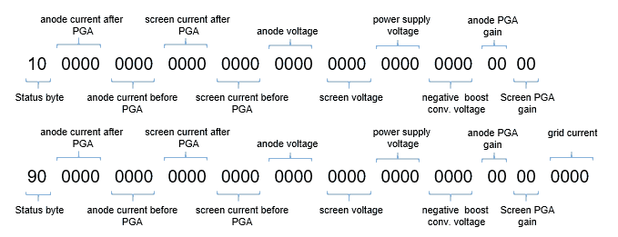
Figure 14-3 Top: Composition of the old result string (without the extension board). Bottom: the result string with the extension board in place.
Quite extensive modifications were necessary to integrate the positive grid bias and current measurement into the GUI. The routine that receives the result string first checks the status byte when it is received. The highest bit is ô1ö 42 characters are received and stored. The current measurement is completely integrated into the GUI and the grid current can be displayed in the same way as the anode and screen currents. Obviously, the grid current is not a part of the quickest. In the calibration form a slider has be designated for the calibration of the positive grid voltage. A text field was added where the positive grid current sense resistor can be entered. As mentioned, the current sense resistor is 4.7 ohm for a current range of 0 ľ 100 mA. With jumper J1 removed the current sense resistor is 33 + 4.7 = 37.7 ohm for a current range of 0 ľ 10 mA. These are the nominal values. The grid current is calibrated by changing the value for the resistances so that the correct grid current is measured.
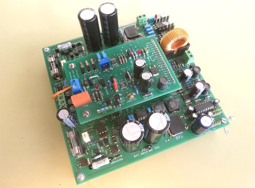
Figure 14-4 Extensive modifications to the GUI were needed to enable the recording, storing, and printing of the grid current. By changing the grid current, the grid current measurement range can be selected.
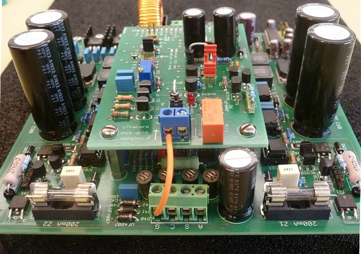
Some impressions of the positive grid extension board. The negative grid output from the main board is connected to the extension board, where a miniature relay automatically selects either the negative grid supply on the main board or the positive grid supply on the extension board. The new grid connection is now the terminal on the extension board.
Examples
This 6146B measures exactly on spec! Notably the transition between triode and pentode region is much sharper than the curves from the datasheet suggest. Although the grid currents for higher plate voltages are ôbang on target,ö the grid current at lower voltages is almost twice the current as given in the datasheet.
The heater of this 812A is obviously exhausted as the maximum current the tube can deliver saturates at 50 mA while it should have reached 600 mA!
Also, this rare TZ-40 has seen better times, although for grid voltages higher than 50V it still tends to oscillate, no wonder with such a spaghetti of wires connecting the tube.

A double tetrode QQE03/12 is a perfect test vehicle for the uTracer6 + extension board. Here it is measured on Derk Reefmanĺs uTracer6!

The internal heater supply of the uTracer6 is a nice gadget, but really only suitable for low to medium power tubes, and as long as there is not a too high demand on its accuracy (although for the uTracer6 the accuracy has increased significantly compared to the uTracer3). Nevertheless, many people prefer to use an external power supply for the heaters of their tubes. For indirectly tubes this can be a DC or an AC supply. However, for directly heated tubes this has to be a DC supply.
The reason is that when a directly heated tube is powered by an AC heater supply the grid to cathode (some virtual point on the heater) voltage varies at a rate of 50 (or 60) periods per second. Since the 1 ms measurement pulse of the uTracer occurs at a random moment with respect to the phase of the mains frequency this introduces significant fluctuation on the measured data.
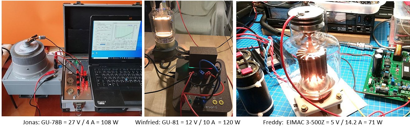
Figure 15-1 Some of the high power directly heated tubes uTracer6 owners are tracing!
It was the testimonial of Freddy that made me realize that many high power transmitter tubes are directly heated and that these heaters very often require enormous power, 100 W or more is no exception. As can be seen in Fig. 15-1, Freddy uses a transformer and a bridge rectifier and some enormous electrolytic smoothing capacitors to obtain a (more or less) DC voltage, but still there was a significant fluctuation on the measured curves. No wonder with a heater drawing as much as 14.2 A heater current!
The circuit
This set me thinking if things couldnĺt be done more elegantly. An obvious solution is to synchronize the measurement pulse with the phase of the AC heater signal. Since I was making modifications to the firmware for the implementation of the positive grid bias option anyway, I decided to add this feature at the same time. Apart from a small firmware modification, which is implemented in PIC firmware versions V6.29 and higher, it only requires a small external circuit.
Figure 15-2 Left: the heater synchronization circuit. Right: connections available on the extension board to interface with the synchronization circuit.
The synchronization circuit is nothing more than a comparator whoĺs inputs are connected over the heater (supply). Every time the heater voltage changes polarity, the output of the comparator toggles. Since the heater has to be connected on one side to the cathode terminal of the uTracer, the average heater potential is basically at power supply level. Therefor I added two voltage dividers to bring the voltages within the input voltage range of the comparator. The output of the comparator is an open collector npn transistor with its emitter connected to the negative supply rail of -15 V. The very simple circuit around T1 brings the output signal to TTL levels. The components are non-critical. For the diode and transistor any small signal equivalents can be used. I guess that instead of the comparator also a decent OpAmp could be used. Very possibly the comparator could also have been ran from a single +15 V power supply, which would allow for tying the open collector output of the comparator directly to pin RC1 of the PIC, but I preferred to use a symmetric power supply. A last minute addition to the PCB of the extension board was a row of pads for a 5 terminal pin header (Fig 15-2 right) for direct connection to the synchronization circuit that I built on a small piece of perf board (Fig. 15-3).
There are plenty of opportunities for experimentation with the circuit. One interesting addition would be the addition of three one-shot delays at the output of the circuit to delay the measurement pulse to exactly 0, 90 and 270 degrees to trace the curves at the extremes of the heater voltage.
Figure 15-3 The heater synchronization circuit (here being tested) is so small that it can easily be built on a piece of perfboard.
Firmware and use of the circuit
At the start of any new measurement, the GUI first sends a ôsettings stringö to the uTracer (read more here). A small modification was made to the firmware such that when the settings string is received, the program first checks if an 50/60 Hz signal is present on I/O pin RC1. This is basically a delay loop of 20 ms. If before the end of the delay loop a low level is detected on this pin, the program knows an AC signal is present, and a flag is set to indicate the measurement routine that after all the voltages have been set, it must wait for a low to high transition on pin RC1 before starting the actual measurement pulse.
The video above shows the synchronization circuit at work. The oscilloscope is triggered by the measurement pulse which is shown in the upper trace. The 50 Hz output of the synchronization circuits is shown on the lower trace. In the first video, the synchronization circuit is not connected to RC1. Note how the measurement pulse occurs at random moments relative to the main frequency. In the second video the synchronization circuits is connected to RC1. Now the measurement pulse occurs at a fixed point in relation to the mains phase, almost at the zero crossing.
Figure 15-4 AC and DC heating compared.
To test the circuit I used my ancient TZ-40. Although the heater of this tube is almost worn out (see previous section), it is one of the few directly heated tube that I have. The left and right column of Fig. 15-4 show traces of the tube powered with a DC heater supply. Note the difference in current between Fig. 15-4 A and D. With the cathode terminal of the uTracer connected to the minus of the heater supply (Fig. 15-4A), the whole heater is above cathode potential. With the cathode connection connected to the plus of the heater supply (Fig. 15-4 D) the whole heater is below cathode potential. In this situation the grid is more positive with respect to the heater resulting in a higher current.
The middle column shows the tube traced with an AC heater supply without using heater synchronization (Fig. 15-4 B) and with synchronization (Fig. 15-4 C). The effectiveness of such a simple circuit is striking. Note how the currents are nicely in the middle of the two DC measurements.
Recently a friend donated me several directly heated triode tubes (DHT) to test the uTracer6ĺs capability of tracing them, especially using a transformer for the heater supply. One of these tubes is the giant 4641 tube, also known as the LK4250 with a different socketconfiguration. The 4641 was introduced in 1937 and could deliver 70 W output power in a class AB configuration. To do that, it operated at anode voltages of up to 1500 V! It was specifically designed to power professional amplifiers e.g. in theatres and cinemas (Fig. 16-1). From the datasheets (no_1, no_2) we learn:
The 4641 is a directly heated output triode with a maximum anode dissipation of 25 W; it has been designed especially for amplifiers with class AB push-pull output. The rated output is obtained only when fixed grid-bias is used. With an anode potential of 1500 V grid bias of -144 V and 105 V (RMS) input to the grids, the output power of a class AB push-pull stage reaches 68 W, at only 1.9% total distortion. The anode current in the absence of a signal is 10 mA per valve, rising to 41 mA per valve when the stage is fully loaded. The optimum anode-to-anode load is 40 kohm. The same circuit but with 1000 V on the anodes and grid bias fixed at -93 V, provides an output of 40 W at 2.35% distortion, for an input of 65 V (RMS). In this case the optimum load is 20 kohm.
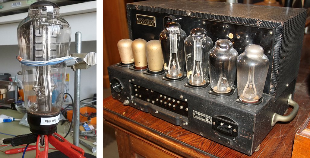
Figure 16-1 Left: The 4641 uses an oversized 4 pin socket to deal with the very high voltages. As I didnĺt have one of those, I used some clips to connect the tube to the uTracer6. Right: A Philips 70 W class AB audio amplifier used in cinemas. The type number on the identification plate is 3760, but unfortunately, I could not find any further information on it. The amplifier is in the Historical Collection (ôStudieverzamelingö) of the Faculty of Electrical Engineering, Mathematics and Computer Science of the Technical University of Delft, the Netherlands. Visit their website and make a virtual tour through the museum which is completely run by volunteers! Photograph by Han Geijp.
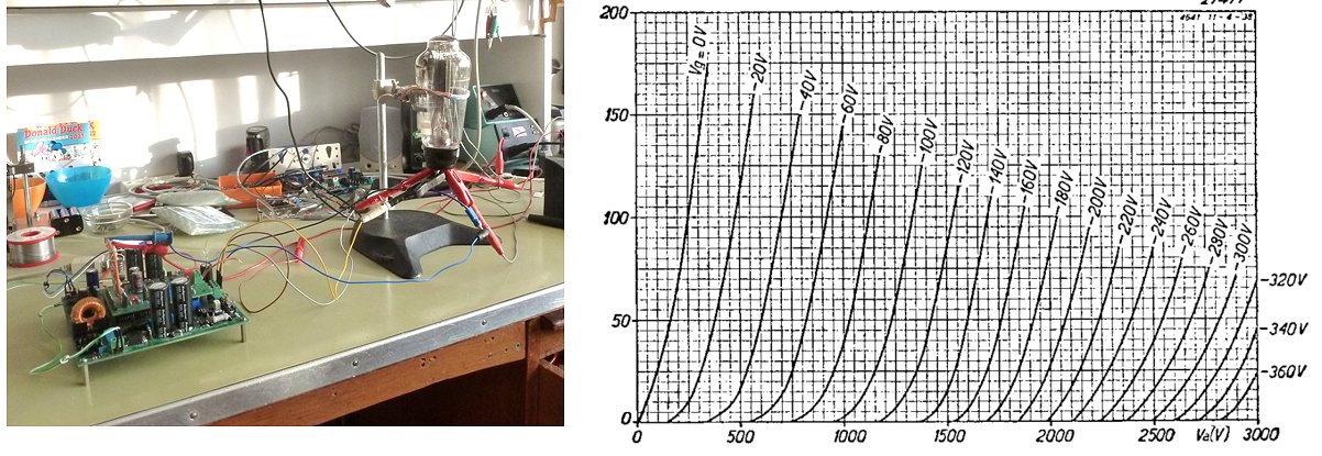
Figure 16-2 Left: The measurement setup with the 4641 connected to the uTracer6. Right: The set of output curves from one of the 4641 datasheets is specified to no less than 3000 V!
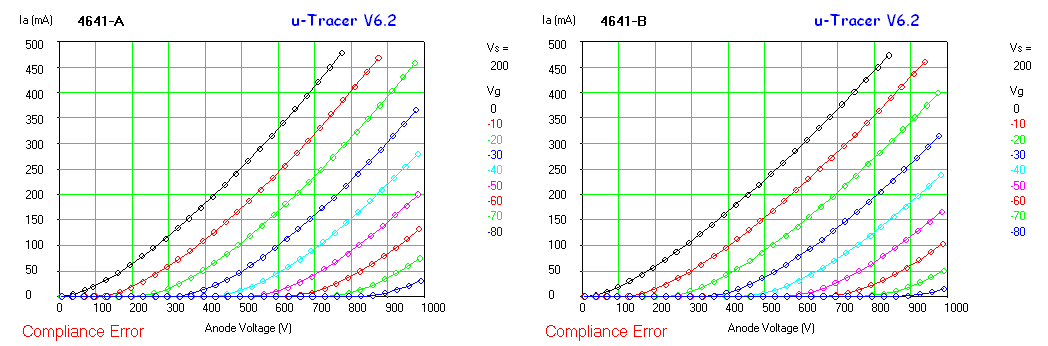
Figure 16-3 My two 4641 traced with the uTracer6. In this case the heater was powered by a transformer, making use of the new feature to AC power directly heated tubes introduced in the previous section. For this measurement I set the compliance to 480 mA, to not unnecessarily stress the filament. Of course, the notice ôCompliance Errorö is not really an error, but a message that the uTracer has skipped measuring the points above the set compliance value (480 mA). To speed up the measurement the range for the screen channel, which is of course not used, was set to maximum, avoiding unnecessary averages. Amazingly, although I can only trace the tube to 1000 V, it apparently is still - after almost 90 years - in tiptop shape!
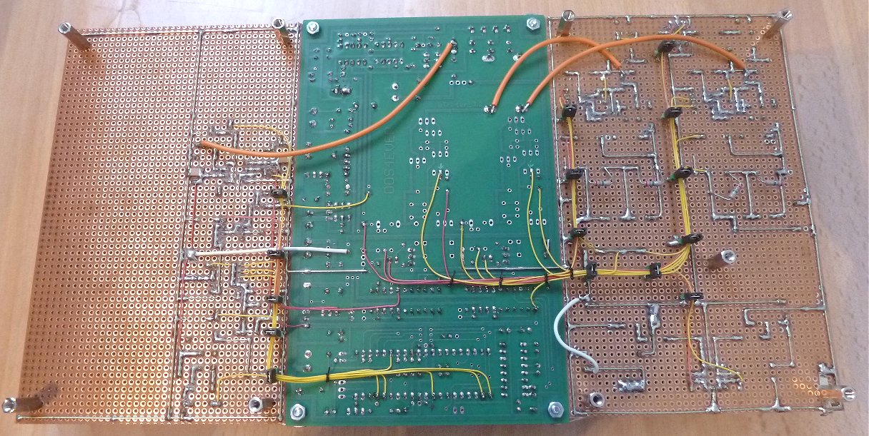
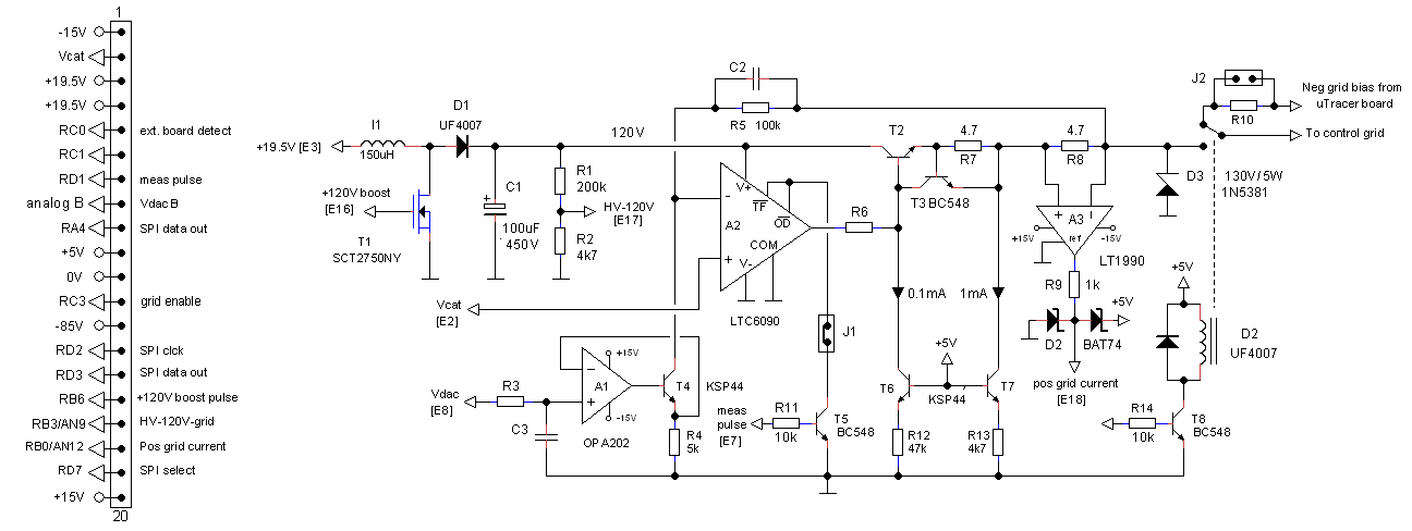