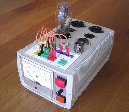
Readers of my pages will not be surprised to learn that, like so many other people, I am fascinated by vacuum tubes. In contrast to most of these tube-lovers I have, at least up to now, little interest in tube amplifiers. I simply do not have the ears for it! I am however fascinated by the technology of these fragile and romantic devices and I love to read and write about their history. I do however have quite an extensive tube collection, and from time to time I am playing with the idea of making a tube tester, or even better a tester which can measure a set of Ia-Va of Ia-Vg characteristics, in other words a tube curve-tracer.
My whole professional life has been devoted to the research, development and fabrication of semiconductor devices. The best term I can find to describe my profession is that of “Semiconductor Technologist.” My interest and fascination for semiconductor technology explain my interest in tube fabrication technology. Radio tube technology has these days almost become an extinct language like classical Latin or Greek, and I
sometimes wonder if also my “craftsmanship” will suffer the same fate? Anyhow, a curve-tracer is about the single most important measurement tool I use in my work both in- and outside the cleanroom. It allows one
 to measure and evaluate very quickly not only transistor and diode characteristics, but also contacts of metals to semiconductors, stability of junctions etc. In short, in my view a curve traces is one of the most useful pieces of equipment around.
The reason why I never actually undertook building a tube curve-tracer is the same reason why I dislike most tube circuits: they are always bulky, heavy, and tend to dissipate a lot of energy! Sometimes the most beautiful ideas come at the strangest moments. In this case it was actually when my mind wondered away during the sermon of the Christmas service in our church on Christmas morning 2010. The idea was very simple: instead of measuring the tube characteristics in a continuous mode, why not measure them in pulse mode?” Pulse mode measurements are frequently done for power transistors in order to be able to characterize the device under biasing conditions which would cause excessive dissipation in continuous mode. The beautiful thing is that when the tubes are measured in pulse mode all of the bulky high voltage power supplies can be eliminated. Instead a low power boost converter can be used to charge up a reservoir capacitor which can easily deliver several hundreds of milliamps during the few milliseconds necessary for the measurements.
The rest of the Christmas holidays were spend on performing the experiments necessary to establish the feasibility of the project. They were encouraging and at the moment I am quite exited about the whole concept. It is a beautiful combination of vintage and state-of-the-art electronics and potentially may even result in something useful. On this page you will find an account of the project as it evolves.
| to top of page | back to homepage |
I believe it was Philips Research Fellow Karel Kuijk who said ‘with a good idea, everything quickly falls into place’ (bij een goed idee zit alles mee). It also applies to this project. Once the idea of a pulsed tube curve tracer was conceived, all the parts of the system seemed to fall into place as if they had been waiting to be put together.
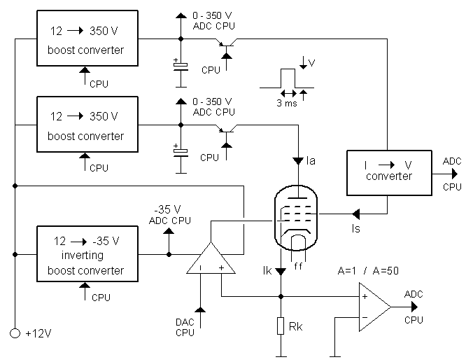
Figure 2.1 Symbolic circuit diagram of the µTracer.
Figure 2.1 shows the initial simplified circuit diagram for the uTracer. For clarity the processor and other digital parts have been omitted. Heart of the uTracer are the pulsed anode and screen-grid power supplies. In a normal curve tracer these would be by far the most difficult and by far the heaviest parts of the tester. They would have to be able to supply a programmable high voltage adjustable between 0 and say 350V at currents up to ca. 200mA. The output power of the anode supply e.g. should be in the order of 50 to 100 Watt requiring a bulky transformer, rectifier and an undoubtedly heavily cooled regulator. By pulsing the anode voltage the whole anode supply collapses into a tiny circuit consisting of only a dozen or so of small components.
The blocks designated “0–350 V boost converter” consists of little more than a 100uH inductor, a diode and a power MOSFET. The gate of the MOSFET is controlled by the microcontroller. The boost converters pumps charge into large reservoir capacitors. The voltage of the capacitors is monitored and adjusted by the microcontroller. Voltages up to 400V can be quite easily achieved this way. At the same time when the high voltage capacitors are being charged, a second – inverting – boost converter generates a negative supply voltage of -35V. This negative voltage is used for the negative control grid bias. Also the generation of the negative bias voltage is completely monitored and controlled by the microcontroller. An analog output of the microcontroller is used to set the grid bias. A single Op-Amp translates the 0-5 V DAC output to a 0 to -35 V grid to cathode bias voltage.
After the microcontroller has charged the high voltage buffer capacitors to the desired values, and has set the control grid bias, it stops pumping the boost converters to eliminate any switching noise and then opens the high voltage anode and screen-grid switches for about 3 ms. After a settling time of 1-2 ms both the cathode current and the screen-grid current are measured. The cathode current minus the grid current yields the anode current. Assuming a maximum anode current of 200 mA, the high voltage capacitor voltage drop during the 2 ms settling time will only drop V = Q/C = (I*t)/C = (0.2*0.002)/(0.0001) = 4 V. This is really a worst case scenario. For most measurements the voltage drop will be much less. Nevertheless, the controller additionally measures the actual anode voltage at the same moment the anode- and screen currents are measured. The cathode current is determined by measuring the voltage drop over a small cathode resistor. A programmable amplifier which amplifies the voltage drop over the cathode resistor enables the characterization of both low- and high power tubes.
| to top of page | back to homepage |
While doing the innitial experiments to study the feasibility of the uTracer project, quite by chance I happened to stumble on a series of articles in some early issues of the Philips Technical Review Magazine describing what are perhaps the first Curve Tracers ever conceived!
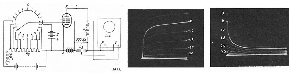
Figure 3.1 A few snapshots from a very early publication describing a curve-tracer mechano-electrical curve tracer [1]. The center picture shows an example a set of Ia-Va curves. The x-axis ranges from 0 – 500V, while the y-axis ranges from 0 – 200mA. The right picture depicts the screen-grid current of the same tube under the identical measurement conditions.
Figure 3.1 shows a few pictures from the first article taken from an article titled ”Applications of Cathode Ray Tubes IV,” from the Philips Technical Review of 1938 [1]. The left figure depicts the circuit diagram of the curve tracer. The anode voltage is derived from a 500 Hz high voltage generator, most likely a mechanical alternator. The stepping voltage for the control grid was generated by a rotating commutator. Ten of the commutator contacts are connected to a resistive divider ladder which provides negative grid biases at equidistant steps which can be adjusted by means of a variable resistor. Note that two of commutator contacts are connected to a fixed negative grid bias of -6 V. So the curve for -6 V is written twice and as a result it will appear lighter on the screen of the cathode ray tube. This fixed curve serves as a reference for the adjustment of the grid bias steps. When the first line coincides with the reference curve, the step is -6 V. When the second line coincides with the reference curve the step size is -3 V, etc. The other contacts on the commutator are connected to the highest negative voltage so that at these positions the tube will be cut-off. The purpose of this is to give the tube time to cool down. Especially during the moments when the anode voltage is low and the screen-grid potential is high, the resulting high screen grid current could otherwise easily overheat the screen grid (Fig. 3.1 right).
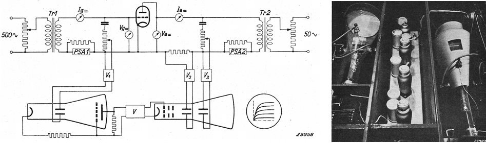
Figure 3.2 A description of this apparatus designed to measure transmitting triodes appeared in the Philips Technical Review of 1939 [2]. The right pictures shows both the normal cathode ray tube (left) as well as the “impulse tube” (right).
A year later in the same periodical an article is published describing a curve-tracer especially designed to characterize transmitter triodes [2]. During normal operation of transmitter triodes, it is quite common that the control grid becomes positive resulting in a significant grid current. It is therefore important that these tubes can also be characterized in that biasing regime. With the previous circuit this was difficult, the grid current would cause spark erosion of the commutator contacts while it would also disturb the proper operation of the resistive ladder divider. For this application the researchers therefore pursued a completely different approach. This time both the grid, as well as the anode are driven by alternating current sources (Fig. 3.2). For the anode a 50Hz source is used, while the grid was driven from a 500Hz power source. Without any further circuitry this arrangement would produce a rather complicated kind of lissajou figure on the screen of the cathode ray tube. The trick was the use of a specially designed “impulse tube.” This was a specially made cathode ray tube (Philips Research had all the fascilities needed to make these kind of special devices) in which the phosphorous screen was replaced by a plate with a second plate with narrow vertical slots punched into it placed in front of it. The x-plates of the impulse tube were connected to the grid voltage, so that only at certain grid voltages the electron beam could hit the plate behind it. This generated a pulse which would turn on the electron current in the normal cathode ray tube which would be otherwise suppressed. So the final set of characteristics was built up from dots corresponding to well defined grid biases. Pretty clever!
Figure 3.3 Click Here to view some more pictures of this amazing beast!
After the war Philips emerged as the dominant tube manufacturer in Europe. The pentode patent in combination with its enormous production capacity all over Europe made its position as the foremost player in this field unchallenged. The center of tube development is the tube-lab in the building in Eindhoven known as the “white-Lady” at the Emmasingel.
Already in a number of other pages I have discussed the organization and structure of this legendary tube-lab, which is otherwise poorly documented. One of the most well-remembered people of the tube-lab is the
 almost legendary Bert Dammers. Dammers headed the group in charge of the development and application of consumer tubes. He wrote several books on radio and television tubes and tube circuits, and was renowned for his ability to think up new and innovative circuits for radio and television in which several functions were combined in as little as possible tubes.
In the Philips Technical Review of 1950 Dammers published an article entitled: ”The Electrical Recording of Diagrams with a Calibrated System of Coordinates” [3]. It should be understood that the Philips Technical Review magazine in the first place was a publication of Philips Research. Nevertheless, from time to time also new developments from the development and application groups appeared in the magazine. The fact that Dammers article was also published meant that it was regarded as an important innovation. The article describes a fully electronic curve-tracer which basically comprises all the ingredients of the modern curve-tracer. The apparatus facilitated in quick and accurate characterization of the many test versions which were fabricated of new tube types. It also allowed characterization of tubes under bias conditions which would under static bias conditions cause excessive heating.
From the description of the system it becomes clear what a tremendous progress electronics had made in the decade 1940-1950. The mechanical commutator which in the earlier designs stepped through the grid biases is now replaced by a fully electronic “stair-case” voltage generator. Such a device was in the tube area already quite an undertaking! The “stair-case voltage” was synthesized by adding a number of square-wave signals which were phase-shifted with respect to each other. A special feature of the curve-tracer was that it also generated a reference grid which would allow for accurate measurements. To even further increase the measurement accuracy two cross-wires could be moved over the screen while the value of the corresponding anode voltage and current could be read from two meters situated directly abode the cathode ray tube. The sine-wave shaped anode voltage was generated by a power amplifier consisting of a balanced amplifier with 2x2 EL34 tubes in parallel. The amplifier could generate 200 W at a maximum output voltage of 620 V!
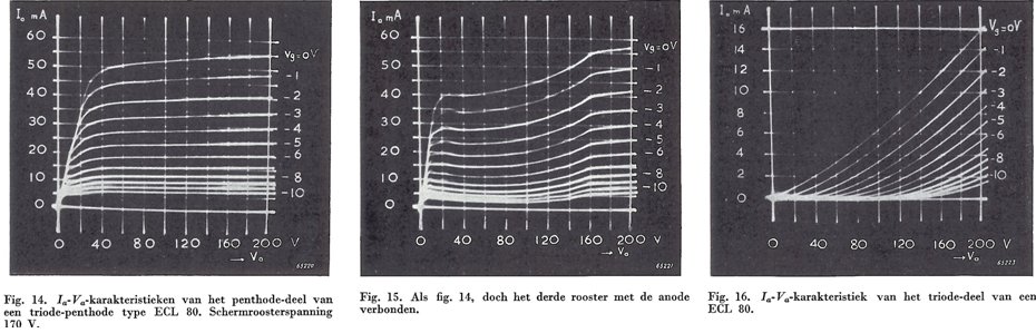
Figure 3.4 As an example of what the curve-tracer of Fig. 3.3 was capable of these measurements on an ECL80 are shown. Left, the pentode section, middle, the pentode switched as tetrode and right, the triode section.
The whole monster comprised some 200 tubes. Assuming an average life-time expectancy of 10.000 hrs for each individual tube, this meant that on average this would result in a system malfunction due to a tube failure every 50 hrs of operation. Therefore the whole system was designed in a modular form so that when a failure occurred the curve tracer could be quickly repaired by just replacing the failing module. At the end of the paper some measurement examples on two state of the art tubes where shown the PL81 (a line output pentode for television) and the general purpose pentode/triode combination tube ECL80 (Fig. 3.4). A nice feature of the pentode section of the ECL80 is that it can be switched at tetrode by connecting the third grid to the anode. I still have some ECL80 tubes lying around, and I have made it my goal to reproduce these curves on the uTracer.
| to top of page | back to homepage |
After that blissful moment of conception that Christmas morning, the remainder of the Christmas days was spent on breadboard experiments to get an idea about the feasibility of the whole concept. Fortunately we didn’t have that many family obligations so there was plenty of time for experimenting. The questions that needed answering were:
The boost converter
Figure 4.1 depicts the test circuit that was used in the first experiments to ascertain whether a voltage in the range of 300-400 V can be achieved with a simple boost converter. The heart of the boost converter is formed by inductor L1, MOSFET T3, and diode D2. For a more complete explanation of the working of boost converters, interested readers are referred to my ”Flyback Converters for Dummies” page. When T3 closes, a constant voltage of 12 V is applied over L1. This causes a linear increase of current through the inductor. Assuming that an inductor of 100 uH is used which saturates at a current of about 2 A, the maximum on-time for T3 follows from:
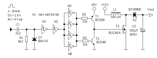
Figure 4.1 Test circuit for the boost converter
With a supply voltage of 12V the final un-loaded output voltage was about 450V. The charging time of the output capacitor strongly depended on the input frequency. For an input frequency of 2 kHz it took for 200V 10” / 300V 40” / 400V 2’. For an input frequency of 20 kHz the charging times drastically reduced to 200V 1” / 300 V 3” / 400 V 10”. So obviously if we want to avoid excessive large charging times, the processor will need to be able to generate such a clock frequency, while at the same time monitoring the capacitor voltage(s). Not impossible, but it need to be taken into consideration in designing the software.
Remaining Issues:
- how to organize the software?
- can the MOSFET be driven directly from the processor?
- how large are the voltage increments per cycle.
Measuring the Screen Current
In the original plan I had, the anode current was measured my measuring the cathode current via the voltage drop over a cathode resistance. This in reality measures the sum of the anode current and the screen current. For normal output pentodes the screen current is usually relatively low compared to the anode current, so the error wouldn’t have been too large. However, for RF pentodes the screen current can be up to 50% of the anode current (e.g. EF94). Moreover, if we measure the full device characteristics to tube becomes biased in regions were the anode voltage is low while the screen voltage is high, under these biasing conditions the screen current can be very high (see e.g. Fig. 3.1). So it is important not only the independently set the screen voltage, which implies a second high voltage boost converter, but also to measure the screen current.
At first this seemed rather to spoil the whole simplicity of the concept. All kind of complex circuits sensing the high-side screen current, translating it to a low side voltage which could be measured by the processor where dreamt up, but none of them very simple. Then I realized that under most biasing the absolute screen current will be still quite small in absolute value. This makes it possible to use a very simple circuit: a good old-fashioned pnp current mirror!
Figure 4.2 The current mirror for measuring the screen-current
Current mirrors are widely used in ICs, but you don’t see them that often in normal circuits. The most left diagram in Fig. 4.2 depicts the pnp current mirror as I have intended it for this application. Note that T1 is switched as a diode, more precisely as the diode in the emitter-base junction. If we neglect for a moment the current flowing to the base of T2, then all of the screen current will pass through the emitter-base diode of T1 and R1, causing a voltage drop. Now first the voltage drop
 over the emitter-base junction. As for any diode there is an exact exponential relationship between the current though this diode and the voltage drop over it. This fact is used in current mirrors in ICs. Here the resistors R1 and R2 are usually omitted and since the transistors are made in the same process on the same wafer and very close to each other, the current voltage relations may be assumed to be identical. Si the voltage drop over the emitter-base junction of T1 will be applied also over the emitter-base junction of T2, causing an identical current to flow through T2! However, if we built up a current mirror with discrete
components, T1 and T2 will be usually not exactly identical. This is the reason why R1 and R2 have been added. These resistors linearize the current-voltage relation of the transistors, making the matching of the currents less dependent on the exact matching of the transistors. But this comes at a penalty. In especially low voltage circuits the additional voltage drop over the resistors is simply not possible, here this fortunately is not such an issue, although it does introduce a small error in the sense that the actual screen grid voltage is a bit less than the set screen grid voltage.
over the emitter-base junction. As for any diode there is an exact exponential relationship between the current though this diode and the voltage drop over it. This fact is used in current mirrors in ICs. Here the resistors R1 and R2 are usually omitted and since the transistors are made in the same process on the same wafer and very close to each other, the current voltage relations may be assumed to be identical. Si the voltage drop over the emitter-base junction of T1 will be applied also over the emitter-base junction of T2, causing an identical current to flow through T2! However, if we built up a current mirror with discrete
components, T1 and T2 will be usually not exactly identical. This is the reason why R1 and R2 have been added. These resistors linearize the current-voltage relation of the transistors, making the matching of the currents less dependent on the exact matching of the transistors. But this comes at a penalty. In especially low voltage circuits the additional voltage drop over the resistors is simply not possible, here this fortunately is not such an issue, although it does introduce a small error in the sense that the actual screen grid voltage is a bit less than the set screen grid voltage.
Using the high side voltage switch (from one of the next sections) the current mirror was tested under pulsed conditions. In this experiment a resistor was used to set the current in the diode branch of the mirror (Fig. 4.2 left b). The current in both branches was monitored by measuring the voltage drop over a 1k21 resistor. With in total 22k + 1k21 = 23.21k in the diode branch, this would set the current to 250/23.21k = 10.8 mA. The voltage drop over the resistors in the left and right branches of the mirror are displayed in the right picture of Fig. 3.2. As can be seen, they are, as far as can be judged from the oscilloscope picture identical. The pulse height is approximal 12.5V corresponding to a current pulse of 12.5 / 1k21 = 10.33 mA. Well within measurement tolerances. So all in all the current mirror idea seems to work quite well for this application.
Note that this circuit can only be used because it is operated in pulsed mode. Suppose e.g. that the screen current is 10 mA and the screen voltage 400 V. This is equivalent to a dissipation of 400*0.01 = 4 W! In pulsed mode the average dissipation is of course reduced proportionally to the pulse / pause ratio. Another point of concern is the maximum value of the screen current. In biasing conditions where the anode voltage is low and the screen voltage is high the screen current can be quite high. The circuit should be able the measure this.
Remaining Issues:
- how small can the linearization resistor be made (to reduce the voltage drop)?
- What is the maximum screen current that can be handled.
The high-side voltage switch
The high-side voltage switch which pulses the high voltage to the anode and screen-grid of the tube is one of the key components of the circuit. It should be able the switch on the voltage quickly enough, and should have a low voltage drop. Basically there are two options for this switch: a high voltage p-type MOSFET or a high voltage pnp transistor. I know that most people would choose for a MOSFET. They can easily handle the currents involved and can have a very low on-resistance. The fact that MOSFETs are relatively easy to understand makes that a lot of people prefer MOSFETs over bipolar. However, the choice for high voltage p-type MOSFETs is not so large and driving a high-side gate is also not that straightforward. I personally prefer bipolars, not in the last place because I have a box with 2000 PN5416 high voltage transistors waiting to be used in a nice circuit!!
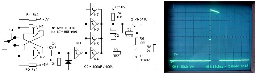
Figure 4.3 Test circuit for the high voltage switch
The first test circuit is displayed in Fig. 4.1. The flip-flop around N1/N2 debounces switche S1. When the switch is pressed, they output of of N2 becomes high. The differentiating network C1, R3 in combination with N3 reduces the pulse length to ca. 10 ms (negative going). Inverters N4 – N7 buffer and invert this pulse. The high-side switch itself is formed around T1 and T2. Just like in the real tube tester the high voltage is supplied by a charged capacitor. The way the switch has been set up is straightforward, in fact too straight forward. R5 keeps T2 off when T1 is not conducting. When high voltage T1 is on, it provides the base current for T2. A dummy load resistor of 2k (R8) is used to simulate a load that would pull about 300 / 2000 = 150 mA at an voltage of 150 mA. At such a high collector current the hFE of T2 will be biased in the high current regime and the hFE will be significantly reduced. Here it was assumed that the hFE was reduced to something like 10 so that T2 needs a base current of about 15 mA to keep it into saturation. Resistor R6 sets a base current of 300 / 22k = 13 mA. The left picture in Fig. 4.3 shows an output pulse of the test circuit for a voltage of 250 V. Quite to my surprise the rise time of the pulse is very sharp, well within 1 ms, which is great because it means that the measurement time can be kept very short. Also observe the discharging of C2 during the pulse.
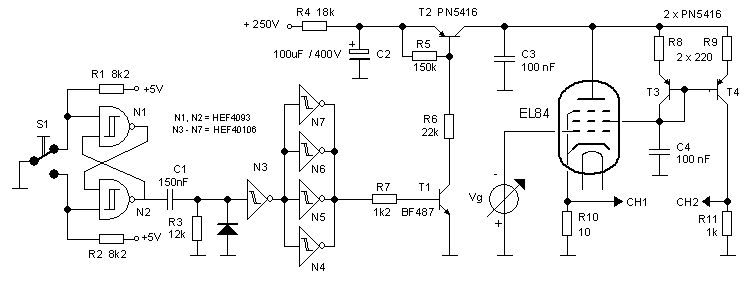
Figure 4.4 First pulsed measurements on an EL84.
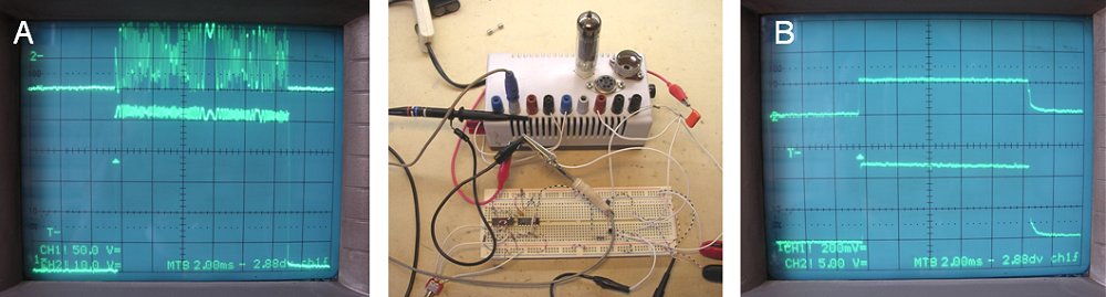
Figure 4.5 First pulsed measurements on an EL84. A. shows the oscillations in anode voltage (bot) and voltage drop over the cathode resistor (top). B. shows Ia (bot) and Ib (top) of the EL84 under typical biasing conditions.
I was so satisfied with this result that I had forgotten to actually check the saturation voltage (or in other words the emitter-collector voltage drop) of T2. Having realized this, the left circuit of Fig. 4.5 was quickly put together to measure it. Since I didn’t want to fool around with potentially lethal voltages unnecessarily, the circuit was operated from 15V. At this point I realized a serious flaw in this circuit: for a given base current (and hence anode current) the value of R1 depends on the voltage of the circuit! So far I had assumed that the circuit would always operate at a voltage of say 200 – 350V. But of course in a curve tracer the voltage may vary between 0 and 350 V! Since the base current is set by (V – 0.9)/R1 with 0.9 the emitter-base voltage drop of T2, the base current would decrease proportionally to the supply voltage, which would make it impossible to measure high currents at low voltages. Anyhow the circuit was used to determine the saturation voltage and the base current needed to reduce it to the minimum. The load resistor of 68 ohm sets a collector current of 16 / 68 = 220 mA. Experimentally it was found that a value of something like 380 ohm for R1 reduced the saturation voltage to a value less than 1V. This corresponds to a base current of (15 – 0.9)/380 = 37 mA.
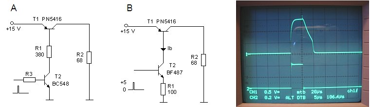
Figure 4.6 Improved driver circuit for the high voltage switch (center) and the voltage pulse over the load resistor (top 5 V/div), and the voltage drop over R1 (bottom 2 V/div).
A much better solution is circuit B in Fig. 4.6. Here T2 is used as a current source whose current is determined by the amplitude of the input pulse and the value of R1. Under the (valid) assumption that the forward emitter-base voltage of T2 is more or less constant (0.9V), the current through R1, and hence the current though T2, is determined by (Vpulse – 0.9)/R1. Since the microcontroller will generate a pulse with an amplitude of 5 V, a resistor of 100 ohm results in a collector current for T2 (which is the base current of T1) of (5-1)/100 = 40 mA. Note that whereas in the first circuit all energy is dissipated in resistor R1, it is now dissipated in T2. Let’s make a worst case calculation. Assume V = 400 V and Ib = 40 mA, in that case the dissipation in T2 equals 16 W. Let’s furthermore assume a measurement pulse of only 3 ms, one per second. This would result in an average dissipation of 48 mW. According to the datasheet of the BF487, it can dissipate continuously 800 mW, corresponding to 800 / 48 = 16 measurements per second under worse case conditions. Figure 4.6 right shows the voltage pulse over the load resistor (top 5 V/div) as well as the voltage drop over R1 (bottom 2 V/div). Note that the saturation voltage is much less than 1V.
Generation of the control-grid bias
For the control-grid bias it was assumed that a range of 0 to -20 V would be sufficient to cover most tubes. This bias needs to be applied with respect to the cathode. Since the cathode current is measured by the voltage drop over a series resistance, some kind of circuitry was needed to correct for this voltage drop. Furthermore the on-chip PWM generator with an output voltage of 0 to 5 V (after filtering) was to be used for setting the negative grid bias.
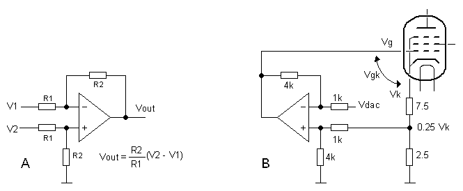
Figure 4.7
It turned out that both requirement could easily be met with a single OpAmp. Figure 4.7A shows the standard OpAmp subtraction circuit. In Fig. 4.7B this circuit is used to bias the control-grid. The resistors in the circuit have been chosen such that the amplification of the circuit is four. The negative input of the circuit is connected to the PWM output (after filtering), while the positive input is taken from a tap on the cathode resistance. The tap is such that it is at exactly 0.25 of the total voltage drop over this resistor.

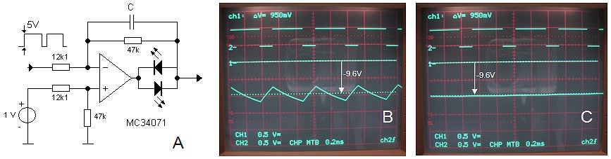
Figure 4.8
A square wave signal with a frequency of 2 kHz, variable duty-cycle and 5 V amplitude was used as input signal. A voltage drop over the cathode resistance was simulated with voltage source. An arbitrary voltage of 1 V was chosen. Resistors of 12k1 and 47k were used because there were readily available. This sets the amplification factor at 47/12.1 = 3.88. As an example a duty-cycle of 70% was used. This effectively means an input voltage of 0.7*5 = 3.5 V. Theoretically the output voltage then follows from 3.88(1-3.5) = -9.7V. The measured output voltage was 9.6, very nicely within all the measurement tolerances.
The negative power supply
With already two boost converters for the anode and screen voltages, it seemed only logical to use a third (inverting) boost converter for the generation of the negative supply voltage for the OpAmps. Figure 4.9 shows the circuit that was used to test the circuit. The working of the circuit is simple. The BC548 npn is driven with the same 15-20 us pulse that is used for the high-voltage converters. This transistor will pull the pnp transistor into saturation causing a linear increase of the current through the inductor. When the BD138 shuts off, the inductor wants to keep the current flowing and the only way it can do this is to reverse the polarity over its terminals so that the diode starts to conduct, thereby negatively charging the electrolytic capacitor.
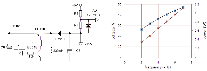
Figure 4.9
Rather unconventionally an pnp power transistor was used instead of a PMOS transistor. The reason is that I didn’t have one “in stock” but that I did have a whole bunch of BD138 transistors. Agreed,a power PMOS transistor would perform better in this circuit, but the performance is not that critical so that a simple BD138 performs good enough. That is the same reason why a simple BAV10 (1N4148) diode was used instead of a fast switching rectifier diode. The circuit was tested using a 2 kohm resistor as load and a pulse width of 15 us. Figure 4.9 right shows the output voltage and the output power as a function of puls repetition frequency. For a repetition frequency of 7 kHz the circuit generates an output voltage of 47 V in 2 kohm at a current of 24 mA (ca. 1 Watt).
The voltage divider(s)
The voltage dividers reduce the high voltages so that they can be measured with the on-chip AD converter which has an input voltage range of 0-5V. They consist of a simple resistive voltage divider and a protection diode. The protection diode ensures that when, for any reason, the input voltage is too high, the voltage on the input of the AD converter is clamped to Vdd.
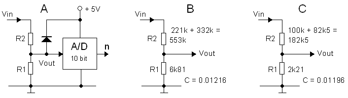
Figure 4.10
The conversion formulas for the circuit including conversion by the 10 bit (0 – 1023) AD converter. Here Vin is the high voltage input, Vout the input voltage of the AD converter, and n the output value of the converter. To ensure the in the datasheet of the AD converter specified acquisition time, the impedance of the circuit connected to the AD converter should not be much higher than 2k. Figure 4.10C is dimensioned for this impedance using 1% resistors. In total the resistance of the divider circuit is in this case 184k. This value is fine for sensing the high voltages after high voltage switches, but the value would be a rather high load for the boost converters if it was used before the high voltage switches. Therefore at that position higher resistance values are used (Fig. 4.10B). This will result in a somewhat higher acquisition time, but when it is a problem the impedance can be decreased by placing a small buffer capacitor over R1.
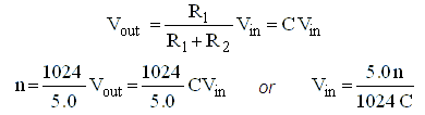
Figure 4.11
| to top of page | back to homepage |
I regularly get emails from people who experience difficulty in starting and completing (!) a project like this. In my opinion (but who am I) the most common mistake leading to disappointment is that most people are inclined to go directly from idea or a paper circuit diagram to an etched PCB. Very often too little time is spend on actually testing (parts of) the circuit. The result is that the circuit does not work properly. Since a circuit on a PCB is difficult to modify it is difficult to debug the project resulting in frustration, and not seldom these people end up finding another hobby.
For all those people some tips that I find useful:
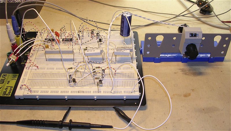
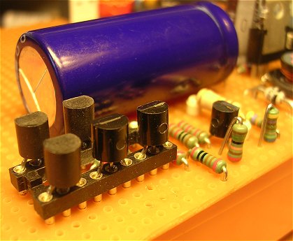
Figure 5.1 One of the best parts of any project: bread board testing! In this case the thyristor protection circuit is being tested.
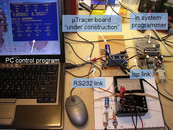
Figure 5.2 When all the difficult circuit parts have been tested on breadboard, everything comes together on perfboard.
After writing all this I can summarize my advice just by saying: “keep things simple, and take small steps at a time.”
Back to the uTracer!
The total uTracer system consists of 4 components:
The Analog Electronics
Many of the sub-blocks of the analog part of the uTracer have already been discussed in the previous section. At the moment “I have pretty strong indications” that some parts will certainly need to be discussed again! However, at this moment the analog part of the circuit as I have it in mind is shown in Fig. 5.3. I you have read the previous section, the circuit will look pretty familiar and straightforward.
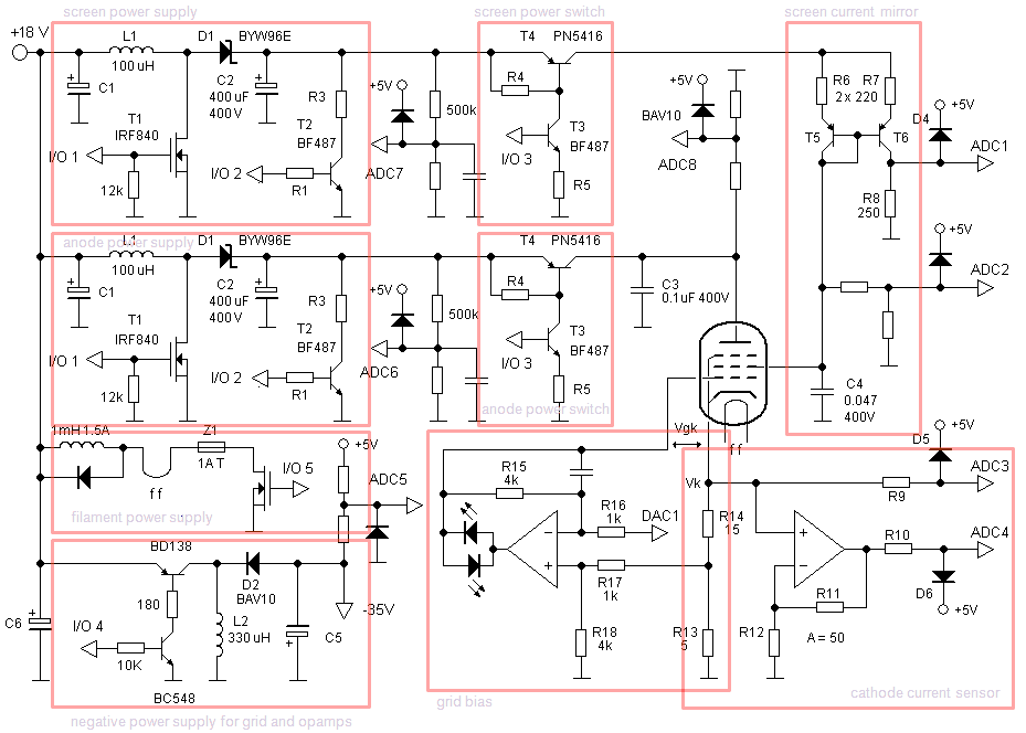
Figure 5.3 Preliminary circuit diagram of the analog part of the uTracer.
The Digital Part
The digital part of the circuit could hardly by more straightforward. The main reasons to use a Microchip 16F874 PIC processor were that I was familiar with it and that it had enough digital and analog I/Os for this applications. For maximum speed and accurate serial communication timing an external 20 MHz Xtal was used. Communication with the PC is via an RS232 link with the “evergreen” MAX232 taking care of the necessary level translations. There really is not anything more to tell about it.
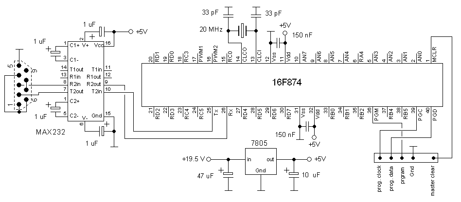
Figure 5.4 The digital part of the uTracer.
The firmware in the microcontroller
I decided to let the PC do the entire user interface so that the tasks for the microcontroller are rather limited. The microcontroller in the first place has to receive the settings from the PC. When the settings are received, it will charge the buffer capacitors in the boost converters and set the grid bias. When the anode, screen and grid voltages have reached their set-point, all boost converters are switched off to reduce noise, and the electronic switches are closed. After a short stabilization time of about 1 ms, all analog voltages and currents are measured as fast as possible after which the switches are closed again. The measured values are then reported back to the PC.
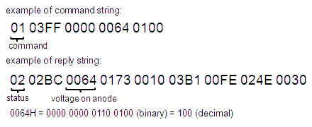
Figure 5.5 Example of the command and reply strings.
The communication protocol between PC and microcontroller is very simple. The PC always sends a command string with fixed length of 18 ASCII characters to the microcontroller, and the controller in return always returns with a reply string of 34 ASCII characters. Figure 5.5 gives an example of the syntax of both strings. Each two consecutive characters in either string represent a byte. The command string first starts with a byte which represents the command. The next two bytes (so four characters) are the set point for the anode voltage in 16-bit binary format. Since the AD and PWM converters of the microcontroller are only 10 bits, only the lowest 10 bits in these 16 bit words are used. The next word (so two bytes = 4 characters) set the screen voltage. The command string is terminated with the grid and filament voltages. The reply string has a similar definition. It starts with a byte which is a status byte. It is followed by 8 words which represent:
The user interface software on the PC
For me, the user interface software is one of the more challenging parts of this project. In the end I want to have a nice windows interface a nice Ia-Vgk graph and all the other features one would expect from a windows interface. From the fact that I have named my website “dos4ever,” it is not difficult to deduce that I have very little affinity (and experience) with windows oriented programming languages. However, for the past year my son Daan (11 years) has been playing with Visual Basic so it cannot be that difficult! In the mean time I have written a simple interface program in good old QBASIC 4.5 (the compiler version). For the past 15 years QBASIC has served me very well in many projects. It is simple, fast and the build-in compiler generates a nice and compact code!
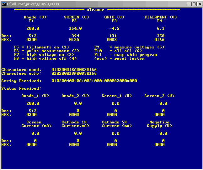
Figure 5.6 A screen dump of the “debug” user interface program written in QBASIC and running from a dos command window.
A Screen dump of the user interface of the program is shown in Fig. 5.6. On the top of the screen the adjustable voltages can be found. By pressing F1, F2, F3 or F4, the setting for the anode voltage, the screen voltage, the grid voltage and the filament voltage can be changed. The program converts the voltage setting to the corresponding AD converter values. In order to calculate this, the AD converter range (0-5V), number of bits (10) and the divider ratio of the resistive voltage dividers are used. Underneath the voltage settings, the corresponding decimal value of the AD converter is given (200V in this case corresponds to 512 decimal) and underneath the decimal value the corresponding hex word is displayed (which is 200H just by chance). Underneath this the commands are displayed which can be issued by pressing one of the other function keys. When a command key is pressed a command string is send to the microcontroller which is displayed in the center of the screen. To check if the controller is functioning properly the echoed character string is also displayed. On the next part of the screen the reply string coming from the controller is shown. This string is taken apart into a status byte and eight measured values, which are again converted to understandable values. The whole program consists of a single loop and was written in a day. It has proven to be a very useful debug tool!
Mainly for my own documentation I have included here a zip file which comprises both the microcontroller firmware as well as the QBASIC (debug) user interface in the state it is at this moment. Which means that only the anode boost converter and switch are implemented. When a command is issued, the buffer capacitor is charged to the voltage which has been set. Then a the switch is closed and after 1 ms the anode voltage is measured and reported back.

Figure 5.7 This picture has absolutely nothing to do with this page, it is just here for my pleasure. A souvenir of a visit to what is claimed to be the largest radio-tube collection in the world in the “studieverzameling” (faculty collection) of the faculty of electrical engineering of the Technical University of Delft. The collection amongst others holds the “Jonker Collection.” Hans Jonker was in charge of the radio tube research at Philips in the fifties, and was also a part-time professor at the Delft University. He brought together a large tube-collection containing many research and development samples. This photograph made Mart Graef (in the center of both pictures) remark: “geluk zit in een doosje” (happiness comes in a box).
| to top of page | back to homepage |
It had to happen sooner of later. I knew from the beginning of this project that the high-voltage switch would be the most difficult part of the circuit. It has to switch voltages up to 400 V with currents up to 200 mA. Moreover, I had set it in my mind that I only wanted to use “small signal” TO92 envelop transistors. The reasoning behind it was that since the pulse width is so very short, excessive dissipation is avoided. Well, I overlooked two things: in the first place devices, especially transistors, heat up much faster than I realized. Secondly, – and this was a much more fundamental thing I overlooked – the switch should be protected against the excessive currents which flow if the output is short-circuited e.g. as a result of a defect tube, unrealistic tube bias conditions, or an operator error. Overlooking both issues, I confidently tested the switch circuit depicted in Fig. 4.4 at maximum voltage and maximum current. It resulted in a nice crisp “pets,” and a flash from somewhere in the switch circuit region after which the complete circuit was dead! On inspection it appeared that not only the transistor in the high-voltage switch had died, but also the power MOSFET, the processor as well as the MAX232! I was very fortunate indeed that both the Laptop as well as the in-circuit PIC programmer where still alive! In short, as our Anglo speaking friends say, ‘back to the drawing board!’ Time for some very serious circuit reflections ......
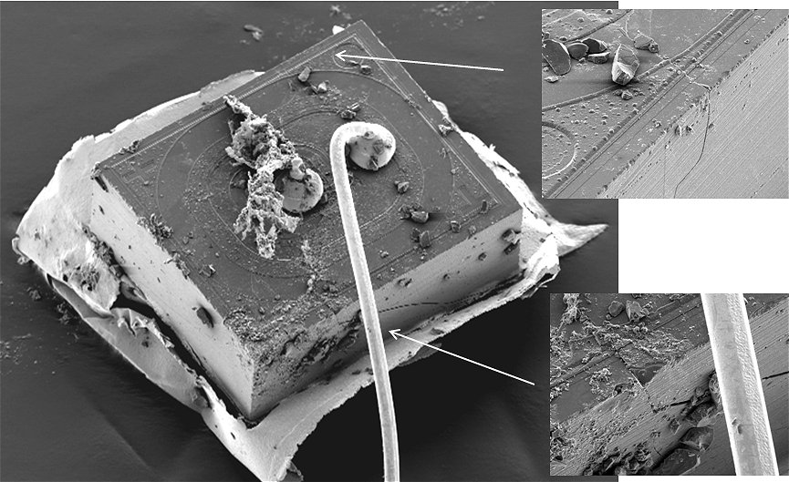
Figure 6.1 A SEM micro-photograph of the BF487 transistor die that failed during testing of the high-voltage switch.
Before diving into the circuit, I was very curious to see what actually happened to the BF487 high voltage transistor when the full power of a 100 uF capacitor charged to 400 V was dumped into the rest of the circuit through this tiny device. To have a look at the actual silicon transistor
 crystal, the plastic package was first dissolved in hot fuming nitric
acid. Now this may sound a bit superfluous, but don’t try to do this at home! Fuming Nitric Acid is a very dangerous highly oxidizing acid, whith very toxic fumes, and you do not want to mess around with it! Although I
have spend my whole working life in semiconductor technology, and have
designed and made quite a number of discrete transistors myself, I am still amazed to see how small the actual transistor die itself is. After dilution of the Nitric Acid and filtration it is sometimes very difficult to even find the remains of the transistor die which measures something in the order of 500 x 500 um. After drying the remains of the
transistor were analyzed with a Scanning Electron Microscope (Fig. 6.1). First of all, this is typically a high voltage transistor. The round shapes and the large overlays of the base metallization over the collector area (field-plates) all help to reduce the electric field and thus to increase the breakdown voltage. It can be clearly seen that the extreme dissipation in crystal caused it to crack and split into at least two parts straight through the middle of the active area. Ok, enough played with the SEM, back to work.
crystal, the plastic package was first dissolved in hot fuming nitric
acid. Now this may sound a bit superfluous, but don’t try to do this at home! Fuming Nitric Acid is a very dangerous highly oxidizing acid, whith very toxic fumes, and you do not want to mess around with it! Although I
have spend my whole working life in semiconductor technology, and have
designed and made quite a number of discrete transistors myself, I am still amazed to see how small the actual transistor die itself is. After dilution of the Nitric Acid and filtration it is sometimes very difficult to even find the remains of the transistor die which measures something in the order of 500 x 500 um. After drying the remains of the
transistor were analyzed with a Scanning Electron Microscope (Fig. 6.1). First of all, this is typically a high voltage transistor. The round shapes and the large overlays of the base metallization over the collector area (field-plates) all help to reduce the electric field and thus to increase the breakdown voltage. It can be clearly seen that the extreme dissipation in crystal caused it to crack and split into at least two parts straight through the middle of the active area. Ok, enough played with the SEM, back to work.
Let’s briefly recall how I arrived at the circuit that just propelled most of my tube-tester circuit into eternity. In section 4 I reported on the first experiments done with the HV-switch. The first experiments involved a simple high-voltage pnp that was pulled into saturation by an high-voltage npn (Fig. 6.2A). Since the transistors in that circuit are either fully conducting with negligible voltage drop or they are completely shut off, the dissipation in the transistors themselves is very low. The circuit was tested at 400 V and currents up to 200 mA. The problem was that the circuit also has to work at low voltages. It is difficult to dimension R1 in such a way that it will safely pull T1 into saturation over the entire voltage range of 20-400V. The solution I choose was to replace T2 with a current source that would supply the required base current, regardless of the supply voltage. The simple circuit of Fig. 6.2B does the trick. The collector current of T2 is now determined only by R1 and the amplitude of the input pulse. The problem now is that the dissipation is in this case shifted from R1 in Fig. 6.2A to T2 in Fig. 6.2B.
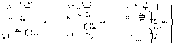
Figure 6.2 High-voltage switch configurations.
Unfortunately I was so stupid only to test this circuit only at 40 V because I was too lazy to build-up the high voltage circuit! The point I totally overlooked was that a resistor, because of its larger mass compared to a transistor, is much easier capable of dissipating high power pulses. The test at 400V and 0.2A caused an instantaneous dissipation of 16 W in T2, and although the pulse lasted only 2 ms, it was enough to destroy it. When T2 short-circuited, the full charge of the fully charged 100 uF / 400 V capacitor, was released in the processor with devastating consequences! The simplest solution to limit the dissipation in T2 is to increase the current gain of the pnp switch. The simplest way to do that is to replace it with a Darlington (Fig. 6.2C). This will approximately multiply the hFE of T1 with the hFE of T2 (at low bias values). Now a base current of only 2 mA is already more than enough to pull the pnp Darlington into saturation. The circuit of Fig. 6.2C was tested over the complete bias and current ranges, and worked very well. However, I realized a serious problem: the circuit of Fig. 6.2C has no protection whatsoever against excessive currents which could flow if the tube is biased in an unrealistic regime or in case of a short-circuit!
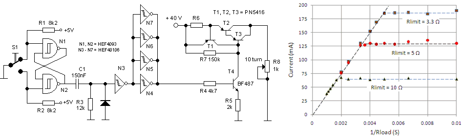
Figure 6.3 Implementation of an overcurrent protection circuit in the high-voltage switch (left), and characterization of the protection circuit at a voltage of 40 V.
The simplest way to implement an overcurrent protection is shown in Fig. 6.3. R6 is the current sense transistor which usually has a small value. When the voltage drop over R6 reaches 0.8-1.0 V, transistor T1 starts to conduct, pulling away base current from the output darlington T2/T3. The higher the output current, the more T1 will conduct, and the further the darlington will be cut-off from base current. When properly designed, this feedback mechanism will result in a constant maximum output current, the value of which is approximately determined by 1.0/R1. The circuit depicted in Fig.6.3 was used to test the concept on a 40 V DC power supply. The load of the test circuit was a 1k ten-turn potmeter. The output current was measured by measuring the amplitude of the voltage pulse over the load resistor with the memory scope. The current was calculated from pulse_amplitude/Rload. As long as the overcurrent protection is not activated the output current should be proportional to 1/Rload, which it is. As soon as the overcurrent circuit is activated, the output current remains nicely constant.
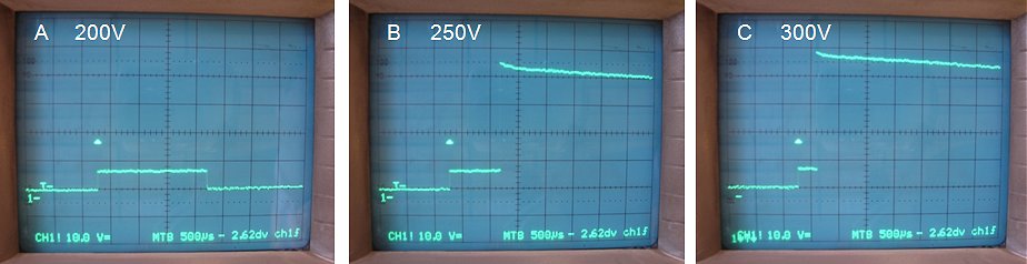
Figure 6.4 Dynamic behavior of the overcurrent protection circuit at high voltages. For voltages higher than 200 V, the dissipation in the pnp transistor apparently reduces the breakdown to such a value that after some time the transistor breaksdown.
The circuit proved to be rather a disappointment when it was tested with the high-voltages that the switch has to control in reality. In this test the circuit was loaded with a 10k resistor, and the current limit resistor was 10 ohm which would limit the current to approximately 70 mA (Fig. 6.2 right), and the current was measured over a 100 ohm resistor. Figure 6.4A shows that for 100 V the circuit worked perfectly. Note that 7 V over 100 ohm corresponds to 70 mA. For 200 V however, the output transistor went into avalanche after approximately 1 ms. Apparently, the dissipation in a pulse even as short as 2 ms causes so much self heating of the transistor that the point of avalanche breakdown is reduced to below 200 V! The situation is even worse for 300 V. A higher voltage results in more dissipation, more self heating and even faster breakdown. The breakdown by the way was non-destructive.
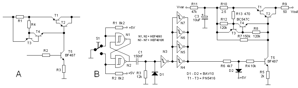
Figure 6.5 This thyristor overcurrent protection circuit abruptly opens the high voltage switch when an overcurrent condition is signaled. The circuit is automatically reset when the pulse is over.
What really was needed was a protection circuit that would turn the power completely off as soon as an overcurrent condition is signaled. To realize this I ended up with quite a simple circuit that I have not seen used before. The overcurrent transistor is simply replaced with a thyristor, build up from a discrete npn/pnp pair. On one of my other pages the two transistor thyristor is discussed in some depth. The principle of the circuit is explained in Fig. 6.5A. When an overcurrent
 condition occurs, the voltage over R1 will increase to such a value that at a certain point T3 will be pulled into conduction through D1. The collector current of T3 is the base current of T4 so that when T3 starts conducting, T4 will also start conducting. However, the collector current of T4 will keep T3 in conduction etc. This condition will persist until the current is completely shut off, which of course occurs automatically at the end of the measurement pulse.
Figure 6.5B shows the practical implementation of the thyristor protection circuit. Resistors R8 and R12 were added to reduce the sensitivity of the thyristor. This sounds a bit strange, but it should be realized that modern discrete transistors are so good that they still have a high current amplification even at nA or pA level. This means that the smallest current spike on one of the bases of the thyristor will cause it to latch. R8 and R12 add a small “base current” resulting at an hFE < 1 for low current levels. As a result a “significant” current pulse of several uA is needed to trigger the circuit. It was found that a voltage drop of approximately 0.66 V over R10 is needed to activate the protection circuit. With R10 = 2.5 ohm the maximum current is 150 mA. Resistor R9 was added to at least have some impedance in the output loop in case of a hard short circuit. Assuming a maximum current of 200 mA, the voltage drop over R10 will be 10 V. especially since the micro controller measures the voltage directly on the anode of the tube, this is not too bad, and we can compensate for it by increasing the output voltage a bit. Finally R4, R6 and D2 were added as a final safety measure to protect the rest of the circuit should the high voltage switch fail. Assuming that for some reason T5 breaks down, the base of T5 becomes directly connected to the high-voltage capacitor which can be up to 300 V. In this case D2 will start to conduct, and R4 will limit the current to 30 mA. Since D2 has a non-zero series resistance this can still mean that the voltage of the anode of D2 is pulled significantly above Vdd. In that case R6 in combination with the input protection diodes on the PIC processor protect the input of the processor for further damage.
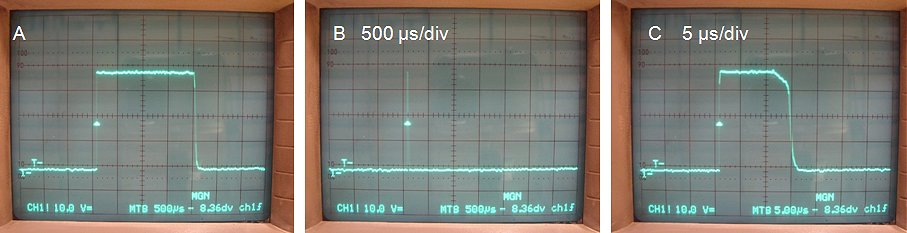
Figure 6.6 Dynamic behavior of the thyristor protection circuit.
Figure 6.6 shows the dynamic switching behavior of the thyristor protection circuit. In Fig. 6.6A the current is below the overcurrent condition value, resulting in a normal output pulse. Figure 6.6B is recorded on the same scale and shows what happens when an overcurrent condition triggers the thyristor. In Fig. 6.6C the short event of Fig. 6.6B is magnified revealing that already after a few micro-seconds the thyristor is activated, thereby shutting-off the output pnp Darlington.
To do some reliability testing the circuit depicted in Fig. 6.5B was modified so that it would “fire” a pulse every second. Then the circuit was tested for several hours on a row for the maximum voltage 350 V under a variety of load conditions, including short-circuited output.
|
Finally a few last words about the construction around R10, R12 and R13 in Fig. 6.5 which, I can imagine, will have raised some eyebrows. The observant reader will no doubt have spotted that resistor R12 has no function whatsoever, given the values of R10 and R13. This is totally true. In the first version of the circuit however, R13 was replaced with a diode (cathode connected to R10) which triggered the thyristor when the voltage across R10 reached the critical value. With the diode instead of R13, the circuit was extremely sensitive to transients and noise. By replacing the diode with a resistor it became much more robust. Despite this modification, the switch remained a rather “difficult” sub-circuit. Although it was tested for all possible load conditions, I noticed remarkable differences between different versions of the circuit (e.g. on breadboard or perfboard) which were apparently due to parasitic capacitances and inductances. A sign which always gives me the very uncomfortable feeling that the circuit is hard to tame, and that there can be problems directly behind every corner.
| to top of page | back to homepage |
After the adventures with the high-voltage switch is became clear that also the current mirror would need a thorough revision. The problem was again dissipation. The simple current mirror as used in Fig. 4.2 uses two transistors. In one of the transistors only the emitter-base diode is used. The voltage drop over this diode isapplied to a second identical transistor which then “mirrors” the current flowing through the first transistor. Since the voltage drop over the first transistor is always limited to a forward diode voltage drop (ca. 1.0 V), the dissipation in this transistor is not an issue. It is the second transistor, the current source, which worst case has to “digest” the maximum screen voltage (300 V) at maximum screen current (say 50 mA). Worst case this could result in peak dissipations in excess of 15 W. In the last section we have seen that this is too much for a small TO92 envelop transistor.
I have to admit that while I am writing these words, I have already abandoned the whole tube tester concept as presented in the previous sections. The problems with the high voltage switch and the current mirrors had given me the uneasy feeling that this was not the right way to go. After some thinking a new concept was developed that didn’t need any high-voltage switches or current mirrors and that was all in all much more elegant. This new concept is presented the next section. Nevertheless, just for documentation sake, a few words on possible solutions for the current mirror.
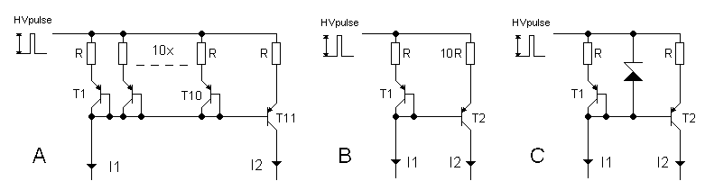
Figure 7.1 Three circuit ideas to reduce / limit the dissipation in the current mirror.
So, how to reduce the dissipation in the current mirror? One solution could be to reduce the voltage drop over the current regulating transistor, e.g. by adding a resistor in series with the collector. In principle this works fine, but it reduces the working range of the circuit. At high currents, the voltage drop over the resistor limits the usable screen-voltage range. The only other option then is to reduce, or at least limit, the current. Figure 7.1 illustrated three possible ways to achieve this. The first, and least elegant way, is to distribute the input current over more than one diode (Fig. 7.1 A). By placing e.g. ten diode-resistor sections in parallel, the input current will divide itself so that each individual diode only carries a tenth of the input current. It is this current which is mirrored by the output transistor. The output current, and thus the dissipation, is in this way a tenth of the original input current. Although the method is quite straightforward and often used in ICs, it is in its discrete form hardly elegant!
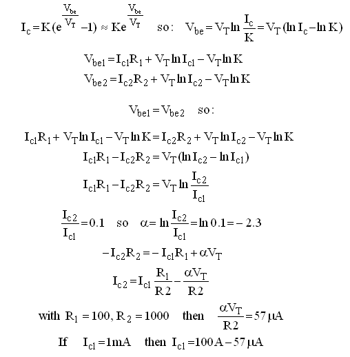
Figure 7.2 First order analysis of the current mirror depicted in Fig. 7.1 B.
A second method makes use of the fact that already some emitter resistors were used to average out any fabrication differences in the transistors. Since the current drop over the emitter resistors determines to a large extend the current, changing the ratio of the transistors can also be used to reduce the mirrored current. Figure 7.1 B illustrates this principle. The input current causes a voltage drop over the emitter-base diode as well as over the emitter resistor. In the mirror branch, this voltage is applied over a resistor with a ten times higher resistivity. As a result the current will be approximately ten times as small. The problem is that the voltage drop over the diodes does not linearly scale with the current. In Fig. 7.2 a first order analysis of the circuit is given. The derivation is quite straightforward and neglects the base resistance. What it boils down to is that there is a “small” error in the output current, which is more or less constant and which reduces for higher emitter resistances. This is logical since for higher emitter resistances the behavior of the mirror will be dominated by the resistors. All in all it does not seem unfeasible to compensate for the measurement error in the software, but again it is hardly elegant.
Finally, in Fig. 7.1 C a brute force method is presented to protect the mirror against too high currents. Depending on the value of the emitter series resistors and the breakdown voltage of the zener diode, the output current of the mirror is clamped to a certain predetermined maximum value. But now, as they would say in Monthy Phyton: “for something completely different”
| to top of page | back to homepage |
Despite the fact that the issues with the high-voltage switches and the current mirror are solvable (and interesting!), they somewhat reduced the simplicity of the concept I had originally in mind. Pondering about this fact, it struck me that there was a very obvious thing I had overlooked. Rather than using quite difficult and critical high-voltage switches implemented in silicon, it is also possible to use the radio-tube itself as the switch! When the control grid is biased low enough so that the tube is completely cut-off, no anode or screen grid current flows and the boost converters can charge the buffer capacitors. By pulsing the grid-bias from the negative cut-off region to the desired (negative) grid bias the current through the anode and screen grid is switched on! This does not require a difficult and fragile high-side switch while the tubes are rugged enough to take pulsed overload conditions should they occur.
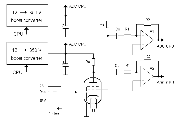
Figure 8.1 In the new concept the tube itself is used to switch the anode and screen. The currents are measured by the voltage drop over a simple series resistors which is AC coupled to the AD converter.
The only problem now left is to find an elegant way to measure the anode- and screen current. Measuring the anode current by measuring the voltage drop over a cathode resistors works but has the disadvantage that the voltage drop over the cathode resistors lowers the anode-cathode voltage. Using a current mirror for the anode current is simply not an option; the currents are just too high. Then a rather nice idea occurred to me which is based on the fact the voltage across a (charged) capacitor cannot change instantaneously. The idea is depicted in Fig. 8.1 and further explained in detail in Fig. 8.2.
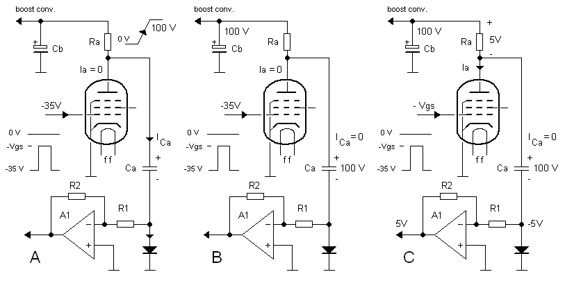
Figure 8.2 AC coupling of the voltage drop over the current-sense resistors is only possible since the measurements are done in pulse-mode.
Basically both the anode and the screen currents are sensed with a simple series resistor (Ra and Rs). These resistors are chosen in such a way that for the maximum current the voltage drop is 5V. Assume for the moment that the uTracer is just switched on, and that the first anode voltage setting is 100 V. The control grid of the tube is held at a sufficiently low potential so that the tube is shut off, and there is no anode- or screen current flowing. The boost converter will now charge the buffer capacitor Cb to 100 V. At the same time Ca will be charged to 100 V with the charge current flowing through the diode (Fig. 8.2A). At a certain moment both Cb as well as Ca are charged to 100V and the charge current will reduce to zero (Fig. 8.2B). Now the grid voltage of the tube is set to the desired bias point. As a result a current will flow through both the anode as well as the screen grid (Fig. 8.2C). This current will cause a voltage drop over Ra which is proportional to the current, in this example 5 V. We assume now for the moment that the measurement interval is so small that the voltage over Ca will not change. In that case the input of the inverting amplifier consisting of A1, R1 and R2 will be pulled to -5 V. When R1 = R2 the amplification is set to -1, so that as a result an output pulse of 5 V will appear at the output of the amplifier. So in this circuit a charged capacitor is used to bridge the potential difference between the “high-side” of the circuit and the “low-side.”
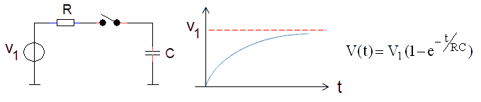
Figure 8.3 Charging of a capacitor.
Since the inverting input of the OpAmp can be regarded as a virtual ground, the time constant which determines the rate at which Ca is charged and discharged is determined by (Ra+R1)Ca. Since Ra << R1 this reduces to R1Ca. One limitation of the “trick” described above is that the time constant R1Ca has to be so large in comparison to the measurement pulse length, that the voltage across Ca indeed not significantly changes during the measurement. On the other hand the time constant should be small compared to the time available for charging of Ca (and Cb). Figure 8.3 depicts how the voltage across a capacitor in a series RC combination evolves after a step wise change in the voltage source. From the equation in Fig. 8.3 we can easily estimate the error introduced as a result of the discharging of Ca during the measurement.
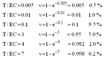
Table 8.1 Charging of a capacitor (equation Fig. 8.3) for some T/RC values.
From Table 8.1 we learn that when T/RC=0.005 the error in the measurement is less than 0.5%. Supposing that the measurement time is 1ms, this corresponds to an RC time of 0.2s. If we for this RC time allow for a realistic charging time of about 1s (T/RC=5), we find in table 8.1 that the charging error is also less than about 0.5%. The application window for which this circuit trick can be used appears to be rather small: a measurement pulse shorter than 1ms is not realistic because we need some time to stabilize the tube and to do the AD conversions, while a longer charging time would result in unacceptable long measurement times. Rather surprisingly the circuit perfectly matches the uTracer design constraints.
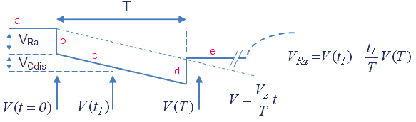
Figure 8.4 Expected voltage drop over the current sense resistors.
There is a second source of error, and that is the discharging of the buffer capacitor Cb during the measurement. Although the buffer capacitor is quite large (100 uF) the voltage drop at maximum anode current can be relatively large. If we assume an anode current of 200 mA, then the voltage drop in 1 ms can be as high as (0.2*0.001)/1E-4= 2V, which is in the same order of magnitude as the voltage drop over Ra. Fortunately there is a simple way to correct for this error. Figure 8.4 shows the voltage at the anode for the circuit diagram depicted in Fig. 8.2. In part ‘a’ of the curve the tube is cut-off and the anode voltage equals the voltage of the buffer capacitor Cb. At t=0 the tube is biased into conduction, and an anode current will start to flow. This current will cause a voltage drop over Ra indicated in Fig. 8.4 by jump ‘b’. During the measurement pulse the anode current discharges the buffer capacitor which is reflected by a linear drop of the anode potential (Fig. 8.4 ‘c’). At the end of the measurement pulse the tube is cut-off again, and the voltage drop over Ra as a result of the anode current disappears so that the anode potential jumps up again (Fig. 8.4 ‘d’). Since there is no current flowing anymore the anode voltage will now remain constant (Fig. 8.4 ‘e’).
Compensating for the discharging of the buffer capacitor is relatively simple. Referring back to Fig. 8.4 the voltage drop we are interested in is given by VRa. However, if the voltage is sampled at T=t1, then the voltage measured is VRa + VCdis. The discharging of Cb is approximately linear so that with and additional measurement directly after the pulse, when the tube is shut-off again, the rate of discharge can be determined from V(T)/T. VRa can now be calculated from the formula given in Fig. 8.4. The only thing to take care of is that the range of the measurement circuit is such that it can measure VRa + VCdis.
In summary, the new concept has the following advantages:
| to top of page | back to homepage |
Although the new concept looked fine “on paper” and contained little uncertainties, it obviously had to be tested. For this the circuit depicted in Fig. 9.1 was used. In this test circuit the tube was replaced by a high voltage power MOSFET which could easily be driven from the micro-controller. In this application it can be considered as an ideal switch. A 1k/5W resistor was used to set the current to a known value. Resistor R4 keeps the MOSFET closed when the output of the microcontroller is in high-impedance state. Resistors R7 and R8 increase the input voltage range of the circuit to 10V.
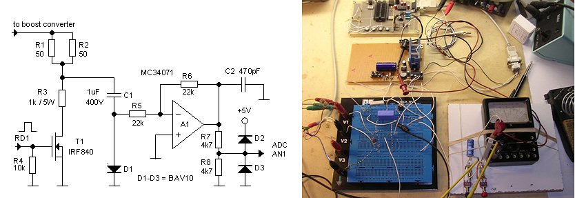
Figure 9.1 Circuit used to test the new concept. The tube is replaced by a high voltage MOSFET and the current is determined by a resistor.
The software of both the controller as well as the program running on the PC were slightly modified to facilitate the experiment. After pressing function key F5, the program produces a pulse on the gate of the MOSFET for 1 ms. Exactly 500 us after the beginning of the pulse the analog input is sampled. Immediately after the pulse the analog input is sampled again. Both values are send to the PC which calculates the corresponding current values and also calculates the current compensated for the discharge of the reservoir capacitor (Fig. 9.3). The first finding was that C1 should be a good quality capacitor, certainly not an electrolytic type. The 10 uF electrolytic capacitor I first tried gave very irreproducible results. The low leakage current of the electrolytic capacitor constantly resulted in a non-zero starting voltage. A 1 uF MKT capacitor on the other hand gave very good results.
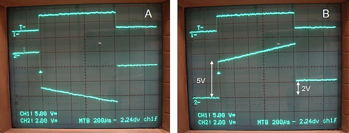
Figure 9.2 Measured voltage drop over the current-sense resistor at the input (left) and output (right) of the inverting OpAmp.
Figure 9.2 gives an impression of the waveforms in the circuit. In this case the reservoir capacitor was charged to 200 V. In the left picture the voltage at the input of the inverting amplifier (node between C1, D1 and R5) is displayed. The upper trace gives the pulse used to drive the MOSFET which signal is used as trigger for the oscilloscope. In the right picture the inverted signal at the output of the OpAmp is displayed. For a voltage of 200 V and a load resistor of 1 k we expect a current of 200 mA. The voltage drop over the 25 ohm sense resistor for 200 mA is 5 V, exactly the voltage drop we find on the scope. For an average current of 200 mA during 1 ms we expect the reservoir capacitor to be discharged by: (I*t)/C = (0.2*0.001)/(0.0001) = 2 V, exactly the value we find at the end of the pulse. Figure 9.3, by way of illustration, shows a screen dump of the output on the PC.
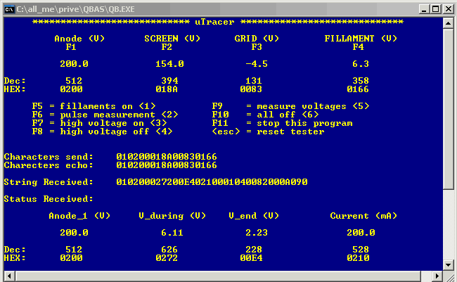
Figure 9.3 Screendump of the output window of the adapted uTracer PC program.
To get an idea of the accuracy of the current sense circuit a series of measurements was performed at different voltages and thus different currents. The buffer capacitor was charged to 50, 100, 150, 200, 250 and 300 V respectively, and at each voltage the MOSFET was pulsed ten times and the current was recorded from the value calculated by the PC control program. The exact current was calculated by first measuring the reservoir capacitor voltage with a multimeter and dividing this voltage by the total resistance (25 ohm sense resistor and 1030 ohm load). It appeared that there was a small offset between the voltage as set by the microcontroller, and the actual capacitor voltage, something I will have to look into later. For each measurement point the difference between the measured current and the “theoretical” current was calculated, and plotted (black dots in Fig. 9.4). Also for each voltage setting the average error was calculated and plotted (red squares and trend line in Fig. 9.4). All in all the error was rather small, most times less than 1 mA, and in all cases better than 1 percent! For the lower currents the resolution of the AD converter added to the inaccuracy. In any case for the uTracer I would say that the results were more than good enough.
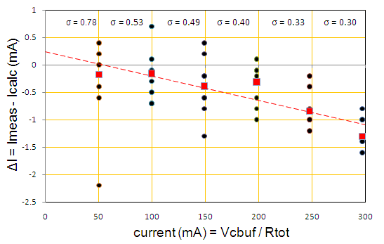
Figure 9.4 In this rather complicated graph, I have tried to assess the accuracy of the current measurement method proposed in the previous section. Like in fig. 9.1 the current was set by the sum of the current sense resistor and the load resistor (= Rtot in this case 25+1030=1055 ohm) in combination with the applied voltage (= voltage of the buffer capacitor Vcbuf). Vcbuf was varied between 50 and 300 V in 50 V increments. For each voltage setting the current was measured 10 times. The difference between the measured current and the calculated current was plotted on the vertical axis. The standard deviation of the current difference is plotted in the top of the graph.
| to top of page | back to homepage |
The experiments in the previous section were a good indication that indeed the new concept might work. The next job was to design a circuit that could produce the necessary control grid pulse which switches the tube on and off. In the off state this circuit has to output a voltage which is low enough to switch the tube fully off (Voff). The first plan was to use a voltage like -25 V for Voff. This is enough to switch most tubes completely off. However, there are a number of tubes which require a significantly lower cut-off voltage. The popular EL34 for instance, requires not less than -55 V (at Va = 400V) to switch it completely off. Therefore I decided to design the circuit for a Voff of -60 V. During the “on-pulse” the output voltage should quickly rise from Voff to any desired control-grid bias voltage between Voff and 0 V (-60V to 0V). The value of Vbias is set by one of the two Pulse Width Modulator outputs of the micro-controller which generate a voltage between 0 and 5 V.
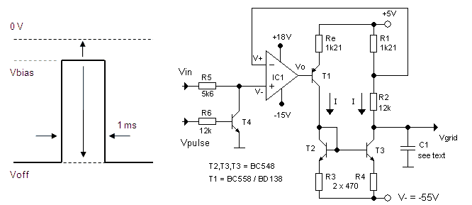
Figure 10.1 Control-grid pulse definition (left) and test version of the pulse generator circuit (right). Note that the component values in this circuit may differ from the final component values.
The most straightforward solution would be to use a high voltage (high power) OpAmp. These high power/voltage OpAmps are however very expensive, and on top of that I prefer to build my projects from “old stuff” I have lying around. So after some experiments with circuits which were oscillators rather than pulse generators, I arrived at the circuit depicted in Fig. 10.1. The circuit is basically a voltage controlled current mirror.
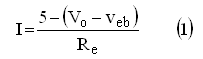
A few words about the selection of the component values: the current range for I was chosen to be 0 – 4.13 mA, for Vin 5 – 0 V. On one hand the current should not be too low because we need some current to switch the control grid, and on the other hand the current should not be too high because that would result in excessive dissipation in the transistors. Most dissipation occurs in T1 when it is biased at maximum current (4.13 mA). In this case T1 dissipates ca. 4.1*60 = 200 mW. It turned out that this was no problem at all for a common BC558 transistor. If desired a somewhat larger BD138 can be used. Resistors R3 and R4 linearize the current mirror so as to obscure small differences between T2 and T3. Note that at maximum current the voltage drop over R3 and R4 amounts to almost 2V. To this one Veb (1 V) a minimal Vcb of 1 V has to be added so that we should reserve at least 4 V for the current mirror. The circuit will perform best if for all resistors 1% resistors or better are used.
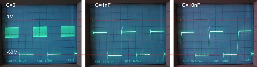
Figure 10.2 Using an MC34071 OpAmp, the circuit of Fig. 10.1 tended to oscillate for certain bias setting. By adding a small capacitor to the output it was possible to suppress the oscillations. If the capacitor is too small, the oscillation is suppressed but there is still and damped oscillation overshoot (middle). If the capacitor is too large the pulse rise time is significantly reduced (right).
The circuit was first tested using a MC34071 OpAmp. The reason I use this OpAmp quite often is that I have a whole box full of them. At certain values for Vbias however, the circuit showed a quite persistent tendency to oscillate (Fig. 10.2 left). By adding ca. 1 nF of capacitance to the output of the circuit the oscillation could be suppressed, leaving only a small (oscillating) overshoot (Fig. 10.2 center). By increasing the output capacitance this overshoot can also be suppressed at the expense of a less steep trailing edge of the pulse (Fig. 10.2 right).
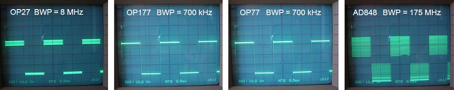
Figure 10.2 Different OpAmp behave differently (obvious!). It appeared that somewhat “slower” OpAmps behaved better with respect to oscillation. A fortunate thing, because low-offset accurate OpAmps usually have a smaller bandwidth.
Experimenting with different OpAmps it was found that in general OpAmps with a smaller bandwidth gave better results with respect to stability. The best choices from the OpAmps which I tested were either an OP177 or OP77. These OpAmps are however rather expensive, but they do have a very small offset. Quite surprisingly the good old 741 proved to be a stable (and cheap) alternative, especially if an external pot-meter is used to compensate for the off-set. Figure 10.3 shows the 741 in action for different pulse heights.
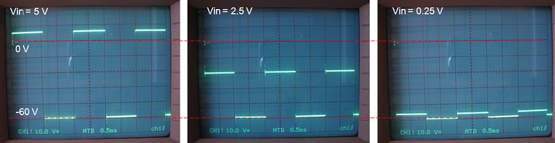
Figure 10.3 A good old 741 OpAmp worked perfectly in this circuit. The Figure shows the output pulse for different input voltages.
At this point the moment had arrived to put several blocks together, to see how the different elements of the new concept would perform in combination with a real tube. The test circuit depicted in Fig. 10.4 brings together the basic building blocks in a way that allows easy testing without the need for a micro-controller. In this case the boost converter was simply replaced by a high voltage power supply connected via a high value resistor R12 to the 100 uF buffer capacitor C3. This construction has the advantage that in case of a short circuit or other accident, “only” the charge of the capacitor is dumped in the circuit.
The anode and the screen-grid are connected to the buffer capacitor via current resistors R13 and R14. The voltage drop over these resistors, which is as we know a measure for the currents, was measured with the memory-scope (input AC coupled). Capacitors C6 and C7 and resistors R15 and R16 simulate the current sense amplifiers discussed in the previous section.
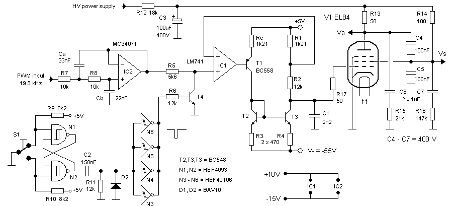
Figure 10.4 Final test circuit to test the “New Concept” on a tube.
The measurement pulse is generated by a simple “one-shot” active low pulse generator circuit which is activated by a push-button. This signal is also used to trigger the memory scope. In the real circuit one of the two PWM generators on board of the micro-controller is used to generate the analog control grid input voltage. Using a 20 MHz X-tal, a frequency of 19.5 kHz is the highest frequency which still allows for 10 bits resolution (see datasheet). To convert the 0-100% duty-cycle PWM square-wave signal to a 0-5 V analogue voltage a low-pass filter is needed.
The design of this low-pass filter was a nice small project in itself. The most important design constraint for the filter is that the output ripple (peak-peak) for a 5 v peak-peak input voltage should be smaller than 1 LSB (5/1024 = 5 mV). Obviously, this can be realized with even a simple first order filter by choosing the corner frequency low enough. The penalty is that at the same time the time it takes for the output of the filter to settle to its final value increases. I personally had no feeling at all for the order of magnitude of these values, but this is typically one of these problems where a circuit simulation program can be of great help! For this kind of problems I always use the good old, almost antique, Micro-Cap program.
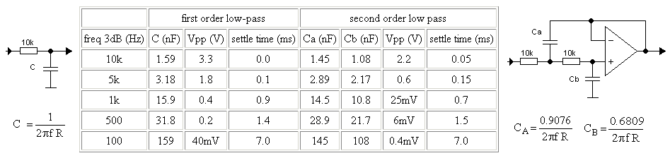
Figure 10.5 Peak-peak output ripple and approximate settling time for a first (left) and second order (right) low-pass filter as a function of corner frequency (freq = 19.5 kHz, Vin = 5 V pp, 50% duty-cycle square wave).
With the Micro-Cap circuit simulation program the peak-peak output ripple voltage (in response to a 50% dutycycle 5V peak-peak 19.5 kHz input signal) and the estimated settling time were calculated for both a simple first order RC low-pass filter, as well as for a second order active version (Fig. 10.5). From Fig. 10.5 it is clear that a first order low-pass filter would require an unrealistically low corner frequency, resulting in long settling times to meet the 5 mV output ripple specification. The second order filter performs much, much better. Already for a corner frequency of 500 Hz the specification is met, resulting in a settling time of about 1.5 ms. Observe that in the final circuit in Fig. 10.4 standard values for the capacitors were used. Simulation showed that replacing the theoretical values with approximate standard values had little effect on the performance. Quite unexpected, but not so strange, the settling time seems to be the same for both the first as well as the second order filter.
The first experiments with the test circuit were performed without capacitors C4 and C5. I knew from the first experiments that the tube could quite easily oscillate, but I had the vague hope that the new concept would be a bit better in that respect. Alas, also this circuit oscillated violently, especially for higher biases. The first thing I tried was to suppress the oscillations with some “chockes” in the anode and screen-grid connections. This suppressed the oscillations a bit for lower biases, but the problem remained for higher biases. Insertion of the two 0.1 uF capacitors C4 and C5 immediately silenced the tube for all bias conditions. Additionally a 50 ohm resistor was inserted in series with the control-grid connection. The circuit was also tested with an EF80 and also for this tube it was free of oscillations over the entire bias range.
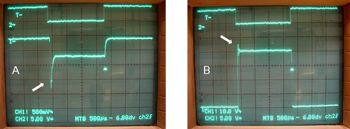
Figure 10.6 A small overshoot in the grid voltage (right) causes a large dip in the anode current (left)
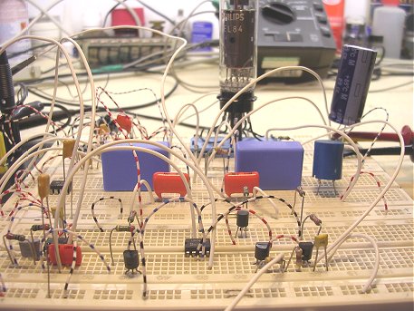
|
| to top of page | back to homepage |
The (hopefully) last remaining nut to crack is the filament power supply. Since I want to use an old 19 V, 3.5 A Dell Laptop power supply as a power source, it is logical to make the filament supply voltage adjustable between 0 and 19 V. Apart from the standard 4, 6.3 and 12 V filament tubes, it is possible to use the tester then also for many of the tubes which have been designed for applications where the filaments are connected in series. Rather than being designed for a certain filament voltage, these tubes are designed for a certain filament current. In the European naming system, tubes starting with e.g. the letter U are designed for a filament current of 100 mA while type numbers starting with a P or X are designed for 300 mA and 600 mA respectively. The filament voltage for these tubes is variable and varies between 4 and 50 V. According to my father’s good old Philips tube manual, a filament voltage between 0 and 19 V can serve 80% of the P type tubes, 60 % of the U type tubes and all of the X type tubes. For the upper limit of the filament current, I have taken the EL34 as a reference. Since I want my tester to be able to “trace” this beast, the filament supply should be able to supply the required 1.5 A (at 6.3 V)!
Controlling the filament voltage with some kind of analog regulator doesn’t make much sense; the dissipation would just be too high. Fortunately, a filament is nothing more than a resistor. This means that we can easily control the effective voltage applied to the filament by pulse-width modulating the 19 V from the power supply. By lucky coincidence we have one PWM output on the processor left over (the other one was used for controlling the grid voltage), so this seems to be the most elegant and simplest solution to control the filament voltage.
It seems so simple, but the PWM control was able to fool me nevettheless! To see how, let’s take a simple example: a voltage source of 12 V is connected via a MOSFET switch to a lamp of 6 V. At what duty-cycle do we have to set the MOSFET switch? Intuitively I assumed it obviously had to be 6/12 = 50 %. So let’s set it at 50 % and measure with an analog voltmeter the voltage over the lamp; it will precisely indicate 6 V as expected. Nevertheless the lamp will breakdown in a few minutes because it is burning way too bright. What is happening? The point is that what is important is not the average voltage which supplied to the lamp, but the average power! The average power supplied to the lamp in PWM mode has to equal the power supplied to the lamp in DC mode, so:
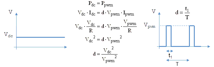
In these equations Pdc, Vdc and Idc are the delivered power, voltage and current in the normal DC operation mode at nominal voltage. Obviously Pdc has to equal the power delivered to the filament in PWM mode when the voltage is pulsed between 0 and Vpwm with a duty-cycle d. The correct setting for the duty-cycle is therefore equal to the square of the ratio of the nominal (DC) voltage and the PWM input voltage. Something I never would have expected.
In its simplest form the whole filament supply could consist of nothing more than a single power MOSFET! There is one small problem: if we do not take any precautions, the peak currents drawn can become very high. Suppose for example that an EL34 is connected to the tester. An EL34 draws about 1.5 A at 6.3 V corresponding to 6.3/1.5 = 4.2 ohm and approximately 9 Watt. An effective voltage of 6.3 V requires a duty-cycle of the PWM signal of (6.3/19)^2 = 11%. Although the average current drawn from the 19 V supply is only 9/19 = 0.47 A, the peak current during the 11% on time can be as high as 19/4.2 = 4.5 A! Additionally, the pulsating nature of this current can disturb the step-down regulator in the 19 V supply. To make things even worse, the “cold filament” resistance will be even much lower. For an EL34 I measured a cold filament resistance of 0.4-0.5 ohm! Normally in a tube amplifier the filaments would be fed from the secondary winding of a transformer. When the amplifier is switched on, the series resistance of the transformer simply limits the current flowing through the filaments until they become a bit heated. The transformer easily survives this temporary short circuit condition, and the soft-start increases the life-time of the filaments. In the uTracer we do not have a transformer, and we will need to simulate a soft-start by slowly increasing the duty-cycle of the PWM signal to the desired value.
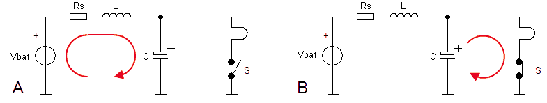
Figure 11.1 Principle of the PWM filament supply and LC filter.
To average out the high current pulses from the PWM circuit an RC or even better LC low-pass filter can be used. Figure 11.1 depicts the PWM circuit in its simplest form. The buffer capacitor supplies the major part of the current when the MOSFET switch is on. The inductor in turn tries to keep the current constant since it cannot accommodate rapid changes of current. When properly designed, the inductor will “re-charge” the capacitor at a constant rate, while the capacitor supplies the very heavy current peaks which occur when the MOSFET switch is on. But what is properly designed? These kind of circuits are rather tricky to analyze analytically, so again the good old Micro-Cap simulator was used to get an idea for component values.
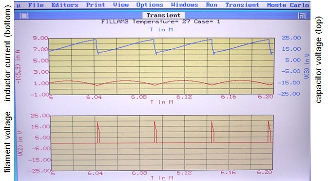
Figure 11.2 Micro-cap simulation of the PWM filament supply with filter (see text below)
Figure 11.2 shows a simulation result from the circuit depicted in Fig. 11.1. In this simulation an inductor of 100 uH with a series resistance of 0.2 ohm was used. The filament was replaced by a resistor of 0.5 ohm. To show what is going on in the filter circuit, a rather low filter capacitance value of 5 uF was used with a 0.1 ohm series resistance. The PWM frequency was 19.5 kHz with a duty-cycle of 10%, the supply voltage was 19 V. The lower trace in Fig. 11.2 shows the current across the filament (resistor). At the beginning of each pulse the voltage is 19 V as expected, resulting in a current slightly less than 40A! The current causes a rapid discharging of the capacitor which can be seen from the rapid decrease in amplitude of the pulse, but also in the upper trace of Fig. 11.2 which shows the capacitor voltage. As soon as the pulse is over, the capacitor is re-charged by the current flowing though the inductor which is shown in the middle trace of Fig. 11.2. This current resembles a double-sided rectified sinusoidal waveform, with its minimum strangely enough at the same moment when the switched is closed.
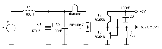
Figure 11.3 Basic circuit of the filament supply.
Since I want to include the complete PWM filament regulator on perfboard pcb without additional cooling of the MOSFET, the dissipation in the MOSFET needed to be kept to the absolute minimum. There are two causes for dissipation: first of all resistive loses in the channel of the FET when it is in the on-state, secondly switching losses. The resistive losses can be reduced by selection of a MOSFET with a low on resistance. Since there is a fundamental trade-off between on-resistance and breakdown voltage, the breakdown voltage of the MOSFET should be chosen as low as possible. The device selected was a cheap AUIRL1404Z from International Rectifier. This transistor is specified for a breakdown voltage of 40 V and an on-resistance of only 4.7 mohm at 5 V gate voltage.
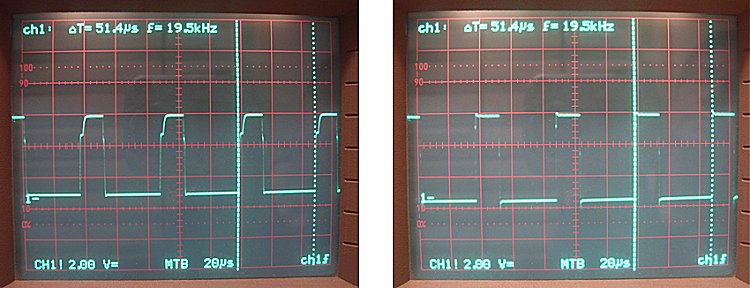
Figure 11.4 Gate drive pulse shape with the IRF1404 directly connected to a PIC output (left) and via the “totem-pole” driver circuit shown in Fig. 11.3 (right).
The dissipation due to switching losses occur because a FET requires a finite time to switch from the off- to the on-state and back. During this transition the transistor is somewhere in between the on-state and the off-state. In this state it dissipates heavily, and the transition from on to off should therefore be done as quickly as possible. In other words: the gate of the FET should be charged and discharged as quickly as possible. Unfortunately low Ron MOSFETs usually have quite a high gate capacitance (a low on-resistance can be obtained by making the transistor large.) The IRF1404 has a gate capacitance of about 5 nF! If we assume that an output of the PIC processor can only source or sink about 25 mA (see datasheet), then the minimum rise time of the gate is something like: 5*5E-9/0.025 = 1us (V*C/I) which is rather long considering the fact that the complete PWM cycle takes about 50 us. Therefore a driver circuit was used to increase the gate drive current and so to increase the switching speed. Several driver circuits were investigated, but in the end I decided to use the “standard” bipolar totem-pole driver circuit [4]. It is very simple, but nevertheless very effective and fast. Figure 11.4 for example shows the gate voltage pulse when the IRF1404 is directly connected to an output pin of the PIC processor compared to the output signal of the simple two transistor “totem-pole” driver from Fig. 11.3.
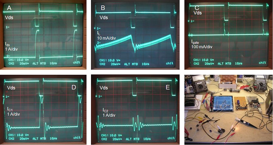
Figure 11.5 The currents in the filament driver circuit measured with a PM9355 current probe.
With a PM9355 current probe and amplifier that I borrowed from work, the currents in the circuit were measured (Fig. 11.5). In all measurements in Fig. 11.5 the drain-source voltage over the power MOSFET is displayed on the upper trace, and it is this signal which is used to trigger the scope. Figure 11.5A shows the current through the filament. The peak current is almost 4A which corresponds nicely to the current we expect given the fact that the filament was biased at a somewhat lower voltage (5.5 V). The ripple current through the inductor (Fig. 11.5B) is only 20 mA. Incredible if you imagine that at the other side of the filter the peak current peaks are 4 A! Also quite revealing is the gate current (Fig. 11.5C). Notice the very sharp peak currents of up to 0.5 A caused by the charging and de-charging of the gate-source capacitance, no wonder a buffer stage is needed! The Figs. 11.5D and E show the current through the electrolytic filter capacitor C1 and the by-pass capacitor C2 respectively. Note that the sum of these two currents (has to) equals the current pulse shown in Fig. 11.5A. It is clear that C2 is absolutely essential in by-passing the parasitic inductance and resistance of C1.
| to top of page | back to homepage |
One of the biggest pitfalls in any project is that after the initial conception of the idea, it is rather difficult to take - from time to time - a step back to critically review the plan. Only after the problems with the “Concept 1 – high voltage switch version,” the idea for the current idea was born. This idea was so much simpler and better that I again fell into the pitfall of not critically reviewing also this plan. But it appeared that there was even a simpler (and better) solution!
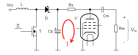
Figure 12.1 Version / Concept 2
Figure 12.1 again illustrates the current (version 2) concept. In summary: the tube itself acts as the current switch while the current is measured by a relatively small series resistance in the anode and screen-grid leads. A capacitor “level-shifts” the voltage pulse over the series resistance from the anode/screen-grid potential to zero volts for further processing. Although the initial experiments have shown that this concept works, it is not ideal either. The level-shift capacitor is large and needs time to charge in between bias changes. Then on the 6th of April René Schmitz from Germany sent me the following email:
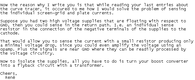
Figure 12.2A illustrates the idea of René. He proposes to use a flyback converter instead of a boost converter so that at the secondary side of the transformer a floating circuit is created, which makes it possible to measure the current by means of a simple series resistor in the ground path. This would completely eliminate the need for the “difficult” level-shift capacitor! The idea is indeed very nice and obvious, and unfortunately I completely overlooked it. The idea actually also works with the simple boost converter circuit (Fig. 12.2B). Obviously all the current flowing through the anode or screen-grid terminal also has to flow through the ground terminal of the buffer capacitor; how on earth could I have I missed it?
Figure 12.2 René Schmitz idea to measure the anode/screen current in the ground lead of the buffer capacitor works for both a boost as well as a flyback converter.
Of the two converters depicted in Fig. 12.2, the Flyback Converter is preferred for at least four reasons:
| to top of page | back to homepage |
After all these experiments and preparations, it is not without pride that I can present here the complete circuit diagram in as far as I now have it. It is certainly not finished yet, and small things may still change. To keep track of these changes, I have added a version number and date to the Figure. The reason this is version 2.x is of course that this is “the new concept design”. Already at this moment I think that there will be a version 3 which has the current sense resistors in the ground connection of the buffer capacitors (see section 12), but since building of this version was already too far underway, I decided to finish this one first. It will be a kind of test version. I am sure that after building and testing of this one there will be many more changes and improvements which together can then be implemented in version 3.

Figure 13.1 Circuit diagram of the analog part of the uTracer (version 3.2 dd. 10-07-2011). Click here to download the circuit diagram in pdf format.
Although all parts of the circuit have already been discussed in the previous sections, some critical components still need to be given their value. The remainder of this section will discuss the “dimensioning” (in Dutch we call this “dimensionering,” I am not sure if dimensioning is the correct English equivalent) of: the voltage dividers in the Boost Converters, the control grid pulse circuit and it’s inverting power supply, and the current sense amplifiers.
The Boost Converter Voltage Dividers
The voltage dividers for the two high voltage boost converters were already discussed at the end of section 4. The voltage dividers reduce the high voltages so that they can be measured with the on-chip AD converter which has an input voltage range of 0-5V. They consist of a simple resistive voltage divider (R4/R5 and R12/R13) and a protection diode (D3,D4). The protection diode ensures that when, for any reason, the input voltage is too high, the voltage on the input of the AD converter is clamped to Vdd.
Figure 13.2 Conversion formulas for the voltage dividers in the anode and screen voltage boost converters.
Figure 13.2 gives the conversion formulas for the circuit including conversion by the 10 bit (0 – 1023) AD converter. Here Vin is the high voltage input, Vout the input voltage of the AD converter, and n the output value of the converter. To ensure the in the datasheet of the AD converter specified acquisition time, the impedance of the circuit connected to the AD converter should not be much higher than 2k. However, to reduce the load on the boost converter somewhat higher resistance values were used. If the high impedances pose a problem the dynamic impedance can be reduced by placing a small capacitor over the lower part of the voltage dividers. Two resistors in series are used for the resistor which takes most of the voltage to prevent arcing. The tolerance of the resistors should be 1% or better. With the resistor values given in Fig. 13.1 the conversion factor is C = 0.01216.
The Control Grid Pulse Generator
The Control Grid Pulse Generator in the final version is designed for two operating ranges: the low range for tubes with a cut-off voltage between 0 and -15 V, and a high range for tubes with a cut-off voltage between 0 and -60 V. In the low range, the grid voltage applied to the tube “in rest” is -15 V, in the high range this is -60 V. The circuit consists of two parts: a programmable inverting boost converter, and the programmable pulse generator.
Figure 13.3 Voltage dividers for the negative grid power supply.
The programmable inverting boost converter has to generate either -20 V for the lower range, and -65 V for the high range. The extra 5 V overhead are needed to correctly bias the npn current mirror in the pulse generator circuit. The processor obviously can only measure positive voltages between 0 and 5 V. The negative voltage is therefore mapped to a range between 0 and 5 V by a voltage divider which is tied to Vdd = 5 V rather than 0 V (Fig. 13.3). Finding the proper resistor values always requires a bit of a puzzling. A good first trial is to map -20 V to 4 V and -65 V to 1 V, this gives both at the low, as well as at the high side a comfortable margin. Some simple math (Fig. 13.3) shows that this is not possible with one set of resistors. The best thing therefore is to go for a compromise, and to aim for something in between: R2 = 20*R1. With R1 = 2k2 this yields 44 K for R2. With a practical value of 47 k for R2, -20 V is mapped on 3.88 V and -65 V is mapped on 1.87 V. The table below summarizes these results, and also gives the corresponding AD values. Note that as a result of the way the voltage feedback is implemented, the boost converter has to be switched on when the measured AD value exceeds the set-point, rather them drops below it as would have been the case in a normal positive boost converter.
| range | Vco (V) |
Vadc (V) |
AD val (dec) |
AD val (hex) |
Vpwm (V) |
Vgrid (V) |
| low | -20 | 3.88 | 795 | 31B | 5 | 0 |
| 0 | -16.20 | |||||
| high | -65 | 1.87 | 383 | 17F | 5 | 0 |
| 0 | -60.34 |
The next step is the dimensioning of the resistors in the grid pulse circuit itself which determine the exact pulse height. The selection between the two measurement ranges is done with a miniature Hamlin relay. When the relay contact is closed, the low (-15/0 V) range is selected, when the contact is open the high (-60/0) range is selected. The formula below was derived in Section 10 of this Page. As shown in Fig. 3.4 the exact resistor ratios needed to exactly come to a -15/0 and -60/0 ranges are R2/R1=3 and 12 respectively. Unfortunately it is very difficult to obtain these ratios even using 1% resistors.
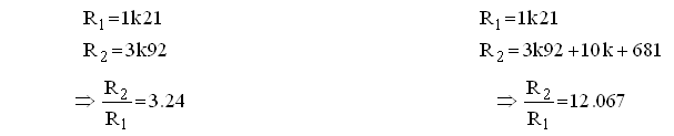
The Current Sense Amplifiers
The resistors for the anode and screen-grid current sensing and the associated inverting amplifiers were a bit trickier to dimension. The voltage at the input of the OpAmp during the measurement pulse consists, as we have seen, of two contributions: the voltage drop over the sense resistors, and the voltage drop due to the decharging of the buffer capacitor. Unfortunately, the latter one is - given the capacitance of these capacitors and the current - a given factor. The problem is that the real anode current has to be calculated from the measured current and the voltage drop of the capacitor. This means that if the voltage drop over the current sense resistors is small compared to the voltage drop of the buffer capacitor, a large computation error will be introduced. The voltage drop over the sense resistors therefore needs to be a few times larger than the capacitor voltage drop.
Let’s take the “high range” anode current as an example. The maximum anode current I want to be able to measure with the uTracer is 200 mA. Given the fact that the measurement pulse will be 1 ms and the buffer capacitor is 100 uF, this implies that the maximum voltage drop of the buffer capacitor will be VBmax = I*t/C = 2 V. The voltage drop over the sense resistor should thus be larger than 2 V, but how much larger? Well, that is a bit arbitrary. We do not want to make it too small, but if it becomes in the order of 10 V, then the error that is introduced in the anode voltage already becomes unacceptable large. As a compromise I took the total voltage drop due to the resistive drop and the capacitor discharge to be 7 V.
After this choice, the values for the components are determined reasoning from the output backward. First of all, the component values for the voltage dividers at the output of the inverting OpAmps IC1 and IC2 are determined. The resistor values for R42-R45 need to be selected in such a way that a voltage range of 0-7 V is mapped on 0-5 V. After a bit of puzzling I arrived at the values indicated in Fig. 13.1. With these values the maximum allowable voltage of 5 V on the input of the AD converter corresponds to 6.91 V on the output of the OpAmp. If we include a safety margin of 0.5 V, and assume a maximum capacitor voltage drop of 2 V at a maximum current of 200 mA, then the voltage drop at 200 mA should be 6.91–0.5–2.0 = 4.41 V. This implies a current sense resistor of 4.41/0.2 = 22 ohm. The nearest 1% resistor value was taken which is 22.1 ohm.
We next reason forward: 200 mA through 22.1 ohm gives a voltage drop of 22.1 *0.2 = 4.42 V. The voltage divider at the output of the OpAmp maps this to 4.42*(3.92/(3.92+1.5)) = 3.2 V. This corresponds to a digital readout of the AD converter of (3.2/5.0)*1024 = 654. The resolution of the whole system therefore is 200/654 = 0.3058 mA/bit. Similar calculations for the other range and the screen current converter resulted in the following table:
| electrode | range | Imax (mA) |
VBmax (V) |
Rsense (ohm) |
V Rsense max (V) |
VAD Rsense max (V) |
AD Imax (dec) |
AD Imax (hex) |
resolution (uA/bit) |
| anode | high | 200 | 2 | 22.1 | 4.42 | 3.2 | 654 | 28E | 306 |
| low | 20 | 0.2 | 22.1+274=296.1 | 5.92 | 4.28 | 877 | 36D | 23 | |
| screen | high | 50 | 0.5 | 121 | 6.05 | 4.37 | 896 | 380 | 56 |
| low | 5 | 0.05 | 121+1k21=1331 | 6.66 | 4.81 | 985 | 3D9 | 5.1 |
After all these tedious calculations we arrive at the following (tentative) design specifications:
| to top of page | back to homepage |
The uTracer hardware including the processor contains very little intelligence. The hardware itself only recognizes 10 bit binary numbers which represent a voltage or current. The hardware receives these numbers in serial format via the command string, and returns the results via a result string. The conversion between an actual voltage setting and the binary number which is meaningful for the uTracer is done by the software in the user interface running on the PC (see next section). Similarly, the binary numbers in the result string one way or the other will need to be converted into current values. This section deals with the conversion formulas residing in the user interface. First the conversion formulas for the command string will be discussed, followed by the conversion formulas for the result string.
The Anode and Screen Voltage Setting
The voltage dividers which reduce the 0-400 V anode and screen-grid voltages to a 0 – 5 V range acceptable for the on-chip AD converter of the microcontroller were already discussed in Section 4 and in the previous Section. Just for completeness the derivation of the equations is repeated here with more appropriate symbols.
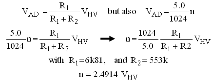
In these equations Vhv represents the high voltage input to the divider circuit (0-400 V), Vad is the AD converter input voltage, and n represents the output value of the 10-bits AD converter. A quick check shows that 400 V corresponds to an AD converter value of: 997.
The Grid Pulse
The equation which gives the control grid pulse height as a function of the input voltage of the pulse circuit was derived in Section 10, and is repeated in Fig. 14.1. The graphical representation of the equation shows that for Vin = 0 V the grid voltage reaches its lowest value which is set by 5*(R2/R1). For increasing Vin the grid bias increases until it reaches 0 at a certain point. Higher grid voltages are also possible but in this version of the uTracer positive grid biases are not allowed.
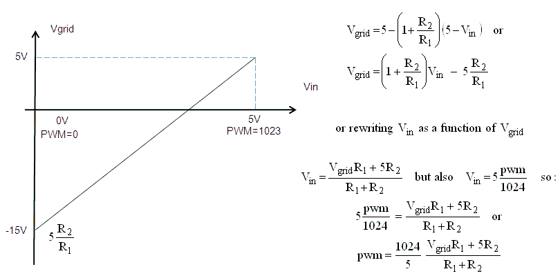
Figure 14.1 Transfer function of the control-grid pulse circuit.
In Fig. 14.1 we have also rewritten the first equation such that it gives the Vin as a function of Vgrid. The input voltage Vin is of course also directly proportional to the duty-cycle of the Pulse-Width Modulated (PWM) signal generated by the microcontroller. Since the PWM generator on the controller has a resolution of 10 bits, Vin can also be written as Vin=5*(pwm/1024). In this equations pwm represents the integer pwm value written into the PWM generator control register, for pwm = 0, Vin = 0 V and for pwm = 1024, Vin equals the supply voltage 5 V. Equating both equations and solving for pwm (Fig. 14.1), we find the expression which gives the pwm value as a function of the desired grid voltage. Since there are two grid bias ranges, two formulas have to be implemented in the software. The formula for the low-range (-15 V) is:
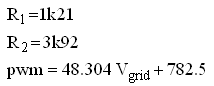
A quick check yield that for Vgrid = 0 V the pwm value is 783 (dec) and that for Vgrid = -15 V the pwm value is 58 (dec). For the high-range (-65 V) the equation is:
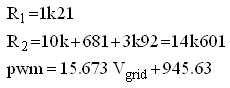
Again a quick check: pwm = 946 gives a grid voltage of 0 V while a pwm value of 5 returns -60 V
The Filament Voltage
In Section 11 it was derived that the RMS value of the filament voltage is a square root function of the duty-cycle. Starting from the derivation in Section 11 it is therefore quite straightforward to come to a formula for duty-cycle as a function of the required filament voltage: Vfilament.
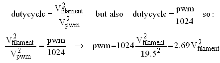
In this equation pwm represents the 0-1023 integer value that has to be written into the control register of the 10-bit PWM generator on board of the microcontroller. Vpwm is supply voltage of the complete PWM circuit, in this case a 19.5 Dell Laptop power supply.
The Anode and Screen-grid currents
The two most important values returned by the uTracer are the anode and screen-grid current values. As explained in section 8 these currents are measured by means of a resistor in series with the anode and screen-grid terminals. A stripped down version of the a single current measurement circuit is given in Fig. 14.2
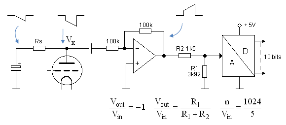
Figure 14.2 Stripped down version of the anode / screen-grid current measurement circuit.
The circuit consisting of the Op-Amp, the voltage divider, and the AD converter basically measures the AC component of the voltage on the anode of the tube. The transfer functions from anode to output of the AD converter and the other way around are very straightforward:
However, as explained in section 8 the voltage pulse measured by this circuit during operation consists of two parts: a more or less constant pulse caused by the voltage drop of the series resistor due to the anode (screen-grid) current, and a by approximation triangular pulse caused by the discharging of the buffer capacitor due to the anode (screen-grid) current. The two components can be quite easily separated by performing two measurements: one approximately halfway the measurement pulse say at time ts, and one measurement immediately after the tube has been cut-off again at tend.
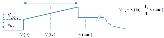
The formula above is used to isolate the voltage drop over the series resistor from the discharging of the buffer capacitor. Once VRs is known, the current obviously follows from VRs / Rs. Here the software should take into account the different Rs values for the anode and screen-grid current circuits and the differences for the high- and low-ranges.
Monitoring of the negative supply voltages
Finally a few words about the monitoring of the negative supply voltages. Although these voltages are controlled by the uTracer, I thought it sensible to also measure these voltages at the end of the measurement pulse and to include them in the result string just for monitoring purpose. Following the definition for R1 and R2 of Fig. 13.3, we find:
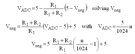
| to top of page | back to homepage |
As the name of my website (dos4ever) suggest, I am not too fond of Windows products. Being somewhat older I feel still most comfortable with small DOS applications that I can understand and that do what I want with a minimum of hustle. If I need to program something, it is usually still good old QBASIC that I fall back to. Nevertheless - if I am very honest - I have to admit that it is sometimes the fear for the unknown which is preventing me from diving into something more up-to-date. About a year ago, my youngest son Daan (11) borrowed a very nice book from the library about programming in Visual Basic (for Children) [5]. During a holiday we went through most of the chapters together, and to my surprise discovered that Visual Basic was not that difficult at all! Within a few hours my son was making all sorts of amusing programs in which buttons on forms moved all over the place with texts insulting the user, and even I could understand what was going on! So from the moment of the conception of the uTracer, it was clear that the Graphical User Interface was going to be written in Visual Basic! The book of my son used the .net version of visual basic. It appeared that with this latest edition of Visual Basic it is rather difficult to access the serial COM ports. After some searching on the web I learned that in Visual Basic 6 this is much easier. That is why I use that version.
As I write these words, my family is going through a very difficult time, since my dear wife has been taken to hospital, and it is likely that she will have to remain there for quite some time. As a result of all this turmoil, the enthusiasm for soldering and experimenting has been rather low the past weeks. Oddly enough I found that engulfing myself in a new programming language, and a rather challenging programming job like the uTracer GUI, took my mind of the problems and helped me to relax. Although the complete program is not finished yet, I thought it best to start writing this section so that I can use it for my own documentation.
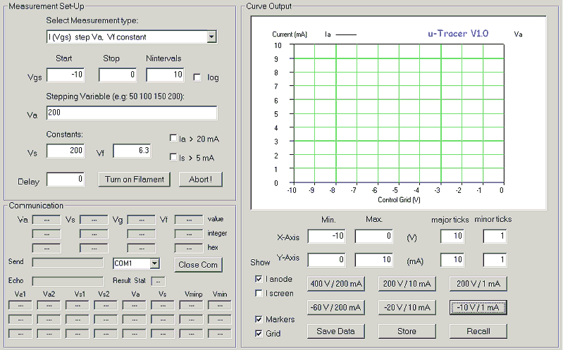
Figure 15.1 Overview of the User Interface Form.
Figure 15.1 shows a screen dump of the User Interface Form. It consists of three parts (Frames in VB language): Measurement Set-Up, Curve Output and Communication. In the Measurement Set-Up, the user selects - via a drop-down (combo-box) menu - what kind of measurement is to be performed. Several types of measurements are possible such as: Ia/Is versus grid voltage, versus anode voltage or even versus filament voltage. If we take the first one as an example, the user next has to define the start and stop values of the grid voltage and the number of measurement steps in which this interval is divided. In normal mode these steps all have the same size, but by ticking the “log” box it is possible to make what is called “a logarithmic sweep.” After the grid voltage range has been set, the user can define the anode voltage(s). By entering more than one value in the “stepping variable” field (separated by spaces), it is possible to measure and draw more than one curve in a single measurement. Finally, the constant biases such as screen grid bias and the filament voltage can be entered, and the user can enter a delay in seconds which is inserted in between every measurement, e.g. to give the filament time to adjust to a new setting.
A logarithmic sweep
Normally, the measurement interval defined by the start and stop values for variable 1 is divided into “Nintv” equal sub-intervals, resulting in “Nintv + 1” measurement points. Sometimes however, it makes better sense to make the spacing between the measurement points at the beginning of the measurement interval a bit smaller, while the spacing can be increased towards the end. An example is e.g. the output characteristic of a pentode where around the knee of the anode current a lot of interesting things are going on, while in the flat – high impedance – part already a few point suffice.
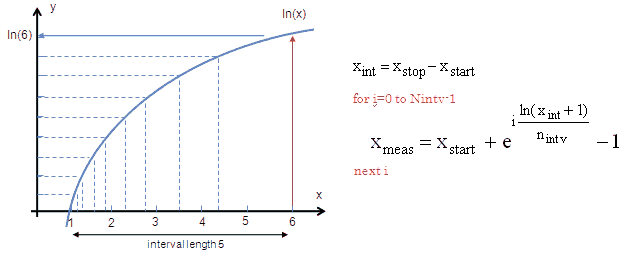
Figure 15.2 Generating a logarithmic sweep
The algorithm to generate a logarithmic sweep is relatively simple and graphically depicted in Fig. 15.2. The basic idea is to project the original interval onto a logarithmic scale via a logarithmic curve, to divide it into equal sub-intervals on this logarithmic scale, and then to project these sub-intervals back to the normal linear scale. The part of the logarithmic curve we use is a bit arbitrary, but for practical reasons it is convenient to take the part where the logarithm is positive starting from x = 1. First the length of the original interval is calculated from Xstop – Xstart. Next the interval is shifted along the x-axis so that it starts at x = 1. In the example in Fig. 15.2 the length of the interval is 5 so that after shifting it starts at x = 1 and ends at x = 6. Next this interval is projected on the logarithmic (y) axis. One is projected to zero while 6 is projected to ln(6) = 1.7918. Next the interval on the logarithmic axis is divided into Nint equal subintervals and the corresponding measurement points on the linear scale are found by exponenting.
The software behind the graphical user interface
The software behind the measurement setup form is relatively simple. After the user has selected a measurement type in the top combo-box, a number associated with the measurement type is transferred to routine “SelectMeas().” This routine sets - depending on the measurement type - a large number of variables: it adjusts the labels next to the input fields, it initializes the input fields to their default values, it sets the minimum and maximum values for each variable the user can enter, and it adjusts the graph in the “Curve Output” frame. The other two important routines associated with the Measurement Setup Frame are: “ProcessVar2String()” and “CheckMeasFields()”. These two routines check the data that the user enters into the input fields.
The way Visual Basic (VB) works is that on every “interaction” of the user with a field or a button (an event) VB executes an interrupt routine which is defined by the programmer. There is an enormous collection of possible events such as: click with cursor on field, move with cursor over field, press key etc. For the buttons the event “click on button” is obvious. For the fields the event to choose was for me less obvious. When do you know the user has entered a new value? I choose two events: the first event is when the user presses the enter key on a field, the second event is when a field “looses focus,” meaning that the user has moved the cursor to another field. Both routines perform the same action, that is that the data is copied from the input field to the proper internal variable and is checked (by routine “CheckMeasFields()”) whether the variable is within the proper range. In case the value is out of range, an error message is displayed by means of a Message Box, and the data is replaced by the default value. Var2 is a kind of special variable in the sense that in this text box a series of values can be entered separated by a space. Routine “ProcessVar2String()” processes this string, checks the values, and stores the values in a matrix.
The Measurements
After the type of measurement has been chosen, and the values for Var1, Var2 and the constants have been set, the measurement can be started. This is done by clicking the “Turn on Filament” command button. This will send a command to the uTracer to switch on the filaments while at the same time the caption of the button will change from “filament on” to “Measure Curve.” It is up to the operator to decide when the filament has reached its final temperature. When the same button is now clicked again, the actual measurement sequence is started. The measurement can be interrupted at any time by clicking the “Abort” button.
The measurement sequence is coordinated by routine “DoMeasurement.” The first thing which happens in this routine is the filling of matrix “dblMeasMX.” This is a two dimensional array in which each row represents a measurement point, and in which each column represents a terminal voltage setting. The matrix is filled by routine “ComposeMatrix.” The routine does three things: based on the settings for Var1min and Var1max and the number of measurements it generates a list of Var1 values (if needed with logarithmic distribution), it combines these values with the values entered for Var2 and finally it writes these values to the measurement matrix “dblMeasMX.” The actual filling of the Matrix is done based on the type of measurement selected because it is at this moment that the values for Var1, Var2 and the constants are assigned to a terminal voltage. So after the completion of routine “ComposeMatrix,” matrix “dblMeasMX” is filled with each row exactly defining a measurement point on the tube curve.
The remainder of the “DoMeasurement” routine is pretty straightforward. In a loop the routine steps through the measurement matrix, and executes each consecutive measurement. First based on the values in a row of “dblMeasMX,” routine “ComposeMeasString” generates an 18 byte string which instructs the uTracer to perform a measurement at the requested settings. The string is send to the uTracer by routine “SndString.” After the command string has been send to the uTracer, routine “RecString” waits for the 34 byte long reply string with the measurement data. This string is analyzed by routine “DecomposeString,” resulting in the anode- and screen current values. These values are stored in the measurement matrix “dblMeasMX” and plotted. After a delay determined by the setting in the Measurement SetUp Frame, the next measurement is executed.
A few points of interest with respect to the Measurement section are worth mentioning. Several measures have been implemented to check for proper operation of the uTracer. The “SndString” routine e.g. checks if the string echoed by the uTracer is correct. Additionally, three timers are used to time the response of the uTracer: an echoed character should not arrive later than 2 seconds from the original character send, the interval between two characters received in the result string should not be longer than 2 seconds, and the time between issuing of the command string and the reception of the result string should not be longer than thirty seconds. These timers have been implemented using the good old “Timer” function which returns the number of seconds elapsed since midnight. The second point worth mentioning is related to the opening of the COM port. Before sending the command string, routine “SndString” first checks if the COM port has been opened already. If it has not been opened yet, the routine opens the COM port specified in the Communications Frame of the form. The final point is related to the “DoEvent” statements in the code. After writing of the routine, I found that it was impossible to interrupt the measurement using the “Abort” command button. The CPU was spending too much time polling the serial interface buffers and checking the Timers! After searching the web for about two days, I found that by adding some “DoEvent” statements at strategic locations, it is possible to force the CPU to handle queued events. It worked like a dream!
The format of the Command String
The command string which is send from the GUI to the uTracer consists of 18 ASCII characters. The first two characters represent the command byte. The next four groups of four characters represent four 16-bit words representing the anode-, screen grid-, control grid- and filament voltages. The command string is not terminated by a carriage return or line feed. From the 16 bit words only the lower 10-bits are used. These ten bits are direct binary representations which mach on-chip AD converter results or which can be directly loaded into the PWM control register. All data conversion or preparation is done by the GUI software. This minimizes the amount of intelligence required in the uTracer itself.
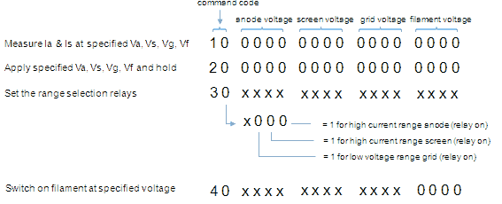
Figure 15.3 Format of the Command String.
Command code “10” initiates a single measurement based on the bias setting in the four data words. After the measurement, this command string is always answered with a result string. Failure of the uTracer to answer with a valid result string results in an error indicated by the GUI. Command code “20” basically does the same without the actual measurement pulse. It sets the anode-, screen- and filament voltages and maintains those voltages until a new command is received. The command can be used for debugging purposes, and the command is also used when the user has specified an additional delay in the measurement frame. In this case the “20” command is issued first (e.g. to heat the filament) and then - after the specified delay - the “10” command is issued. The “3X” command code controls the range selection relays in the uTracer hardware. Which relays have to be switched on is coded in the lower nibble of the command code (Fig. 15.3). When for example code “33” is send, the anode- and screen-grid current range relays are activated, while the control-grid bias relay is not. A bit being “1” always means activation of the relay. The four data words in the relay control string are send, but ignored by the uTracer. Command code “40” switches on the filament of the tube. Again the four data words are sent, but only the last word representing the filament voltage is used. The “20”, “3X” and “40” command strings are not answered with a result string.
The format of the Result String
The result string has a similar format as the command string. In total it consists of 34 ASCII characters of which the first two represent a status byte while the next 32 characters consisting of eight groups of four characters represent eight 16-bit data words. For the status byte so far only one code has been implemented (10Hex) which means a successful measurement. The first two data words represent the contents of the AD converter after measuring the anode current halfway the measurement pulse and after the measurement pulse. The next two words represent the same but then for the screen-grid current. The next four words represent the voltages of the buffer capacitors of the anode and screen-grid supply, the negative supply of the control-grid pulse generator, and the general negative power supply. These last four words are not used by the GUI software, but were just added for diagnostic purposes. Since a measurement will only start when these supplies have their nominal values, the effect of the measurement on the charge in the capacitors can be evaluated.
A Short User Manual
I have tried to keep the operation of the uTracer as simple as possible. The GUI form is divided into three frames: The “measurement setup” frame, The “Curve output” frame and the “Communications” frame. A measurement starts by selecting a measurement type (Fig. 15.4). Selecting a measurement type automatically loads the default values for the different measurement variables. The primary variable is the variable which is plotted against the X-Axis. For this variable the start and stop values can be modified, together with the number of measurement points. By default these measurement points are equally distributed over the measurement interval. By checking the “log” checkbox a logarithmic distribution is generated. In case more than one curve is measured e.g. when a set of Ia(Vgrid) curves is measured for different anode voltages, these anode voltages can be entered in the field titled “stepping variable.” The values in this field need to be separated by a space.
Figure 15.4 The Measurement Setup frame.
There is at this moment no automatic range selection implemented. When the user expects the anode current to be higher than 20 mA, or the screen-grid current to be more than 5 mA, the appropriate checkbox has to be checked. This automatically means that all the measurements are performed with the uTracer set in the high range, and thus with the lower resolution. If the currents are below the indicated values it is therefore better to leave the boxes un-checked and go for a higher resolution. Finally, a delay can be specified which is added in between every measured data point. This delay can be used e.g. in an Ia(V_filament) measurement, to give the filament time to reach its equilibrium temperature.
The command button marked “Measure Curve” in Fig. 15.4 has a double function. Before the first measurement, its caption reads “Turn on Filament.” When it is clicked, a command string is send to the uTracer to switch on the filament with the filament voltage specified in the first entrance in the measurement matrix. When e.g. a filament voltage sweep is made from 1 to 10 V, the first voltage applied to the heater is 1 V. In most cases the filament voltage will obviously be constant, so that the constant value is used. After the “Turn on Filament” button has been clicked, its caption changes to “Measure Curve.” When it is clicked again, the actual measurement is started. When the “Abort” button is clicked the measurement is stopped at once, but the filament is still on. Clicking the “Abort’ button again also switches off the filament.
Figure 15.5 The Curve Output frame.
The “Curve Output” frame displays the measured data. By default only the anode current is displayed (solid line, open markers). By (un)checking the “show Ia / Is” boxes any combination of Ia / Is curves can be plotted. The Is curve is represented by a dotted line with open markers. Below the graph the minimum and maximum values for the axis can be entered. Some elementary checking of the entered values is done based on the selected measurement type. The upper row of preset buttons offers the possibility to quickly change the axis of the graph for Ia(V_anode) type of measurements. The lower row of preset buttons is meant for Ia(V_grid) type of curves.
By clicking the “Save Data” button the entire measurement matrix is written to an external file for further processing e.g. in Excel. Each row in the data file - which has the extension *.udt (uTracer data file) – represents a single measurement. The first column gives the measurement number within each curve, while the second column gives the curve number. The next six columns give the anode- and screen currents (in mA), and the grid, anode, screen and filament voltages. By clicking the “Store” button, the entire measurement matrix is copied into a second data matrix (dblStoreMX) which is internal to the program. By clicking the “Recall” button the stored data in this matrix can be added to the plot (closed markers). In this way it becomes possible to compare characteristics of different tubes. After the “Recall” button has been clicked, its caption changes to “Dismiss”. Clicking it again removes the stored data from the graph, but does not erase the stored data.
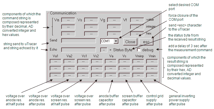
Figure 15.6 The Communications frame.
The last frame, the Communications Frame, has been added mainly for debugging purposes. It allows for a detailed examination of the communication between the GUI and the uTracer. The only input fields are a dropbox which allows the user to select the desired COM port number, a command button to force closing of the COM port, and a check box which when checked introduces a 2 seconds delay after each measurement command (used for debugging purposes). The top row of label boxes shows the values of the bias settings for the current measurement point. In the row below that these values have – using the formulas presented in the previous section - been translated into 0-1023 integer values which are used by the uTracer to set a PWM generator, or for comparison to an AD value. The third row shows the hex format in which these numbers are send to the uTracer in the command string. The command string itself consisting of a command byte and the four hex numbers is displayed in the box “Send”. The characters in the command string are send one by one, and after each character the GUI waits for the echoed character. This whole process is displayed in the two boxes “Send” and “Echo” to allow for monitoring of the handshake process, although the process is usually so fast that it seems as if the strings appear instantaneously.
In the bottom three rows the return string is dissected. As explained, the return string consists of a status byte followed by eight numbers which follow the format explained earlier. Again the top row contains the hex presentation, the middle row the corresponding integer number, while the bottom row contains the measured quantity in normal decimal format using again the conversion formulas presented in the previous section. If for one reason or the other a character is lost in the communication with the uTracer, it is possible that the uTracer remains waiting for a character that will never arrive. To reset the uTracer in such a case the “esc” button can be used. This will send an “esc” character to the uTracer. Reception of an esc character will always force a reset of the uTracer.
Version 1.0 and version 1.t
After a bit more than a month programming it is not without pride that I can present here Version 1.0 for Downloading! Since the uTracer hardware is not completely finished at this point only some elementary back and forth communication of the GUI with the uTracer is tested. The transmission speed of this version is 9600 baud. Undoubtedly the GUI will need some further debugging and modifications, but nevertheless I post this version here as a starting point. The zip file actually contains two versions “uTracer_1p0” and “uTracer_1pt”. The 1pt version is a test version of the 1p0 version. It allows for “playing” with the GUI without any hardware connected. When the 1p0 version is started and a measurement command is issued it will immediately give an error message since it does not receive an echoed string in return within 2 seconds. The test version does not check for echoed characters, and also receives a “simulated” string, which returns a fixed anode current of 7 mA and a screen-grid current of 2.5 mA. To run (or play) with either version just unpack the exe file into a directory and double click the file. To get started with the Test (play) version, after starting check the “debug” check box and click the “Turn on Filament” button. The command to heat the filament is now issued. Clicking the “Measure Curve” command button will now start the measuring sequence.
| to top of page | back to homepage |
At last the moment has come to put everything together. My wife is back from hospital and she is doing reasonable well so I am gradually regaining the peace of mind to heat-up the good old soldering iron again. The circuit diagram is pretty much fixed and ready, but nevertheless, while putting everything together, some small mistakes and omissions were found which in the mean time have been corrected in Fig 13.1 (which also can be downloaded by clicking here.)
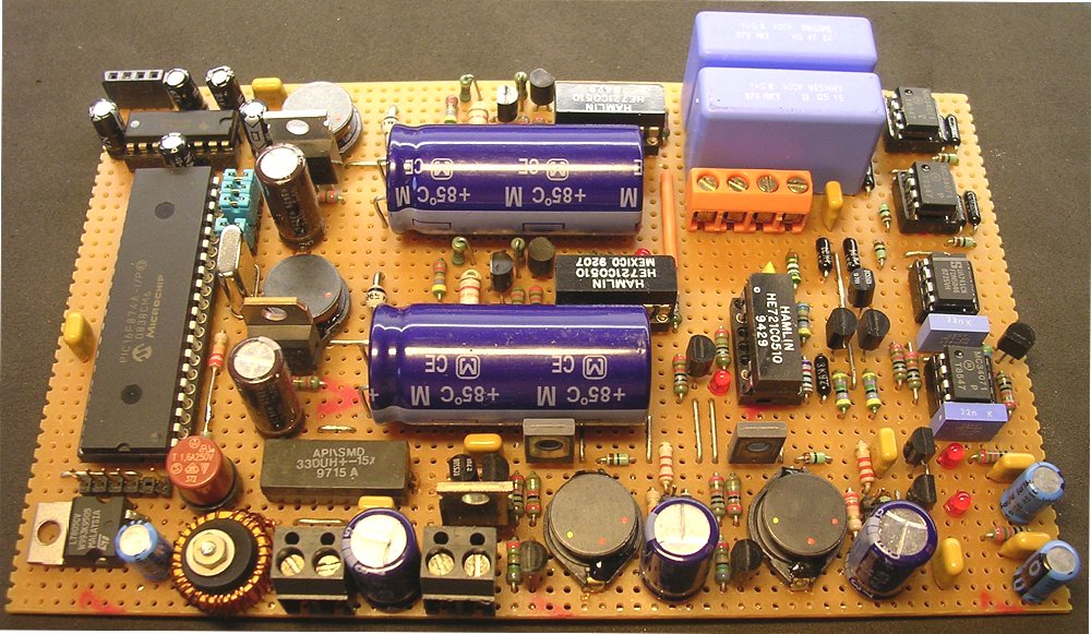
Figure 16.1 The total uTracer hardware!
There really is not so much to tell about the building of the circuit. As always I used a perfboard which worked fine. Special care was taken to have sufficient isolation between the parts of the circuit which carry a high voltage and the rest of the circuit. The placement of the components on the small eurocard format board was a bit of a puzzle but worked out fine in the end. Since the currents in the filament supply circuit can be very high, it was placed directly next to the power supply input, and all wiring was kept very short. The fuses were placed off-board since they took up too much space.
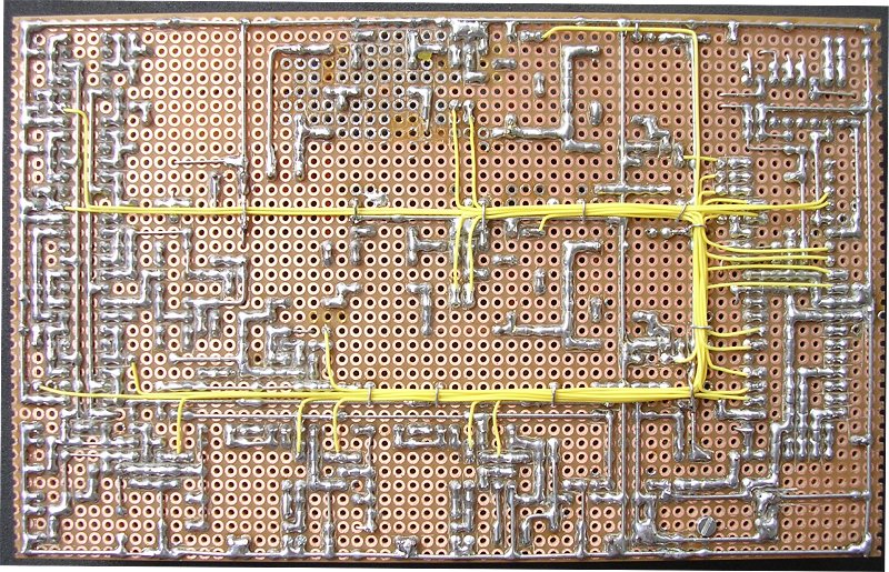
Figure 16.2 The “wiring” side of the perfboard.
As already mentioned in Section 5, the best way – at least for me – to realize such a complex system is to do it step-by-step. So the building of the complete circuit was realized in steps, and each step was tested when it was completed. The processor and the anode voltage supply were already there. They had already been tested in the previous experiments. The first step was to copy the anode boost converter for the screen supply. Next came the filament supply. After some puzzling with the component placement the whole filament supply was realized using not more than a few square cm of pcb area. Amazing how such a small circuit can handle Amps of current. Before proceeding the filament supply was vigorously tested using the processor as the PWM generator and the test program developed earlier in Section 11. It worked like a dream. The power MOSFET remained absolutely cool, even for a 6.3 V / 1.5A load.
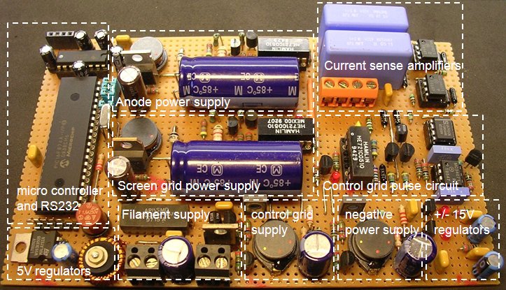
Figure 16.3 The floor plan of the uTracer.
Next the negative power supply for the grid was implemented. It was tested using an external pulse generator set at 20 us pulses at a 100 us repetition and a resistor as load. It behaved exactly as the breadboard prototype. In a similar way all the other circuit parts were put together one-by-one. Then came the moment when the complete hardware was finished. The last step now is the firmware in the processor and, of course, debugging of the whole system.
For the firmware I fortunately didn’t have to start from scratch. Most of the routines written for the “concept 1” version could be re-used without modification (see section 5 and download). At the heart of the firmware are the routines which control the no-less-than four boost converters. These routines will be described in the next section. These routines are a bit tricky, and an error can easily result in destruction of the hardware. For that reason four jumpers were inserted between the controller outputs and the boost converter hardware. The procedure now followed was to gradually expand the firmware and to test the interplay between firmware and hardware bit-by-bit. At this point “two most peculiar problems” were encountered. I will discuss one of these problems in this section, and will save the other one for the next section.
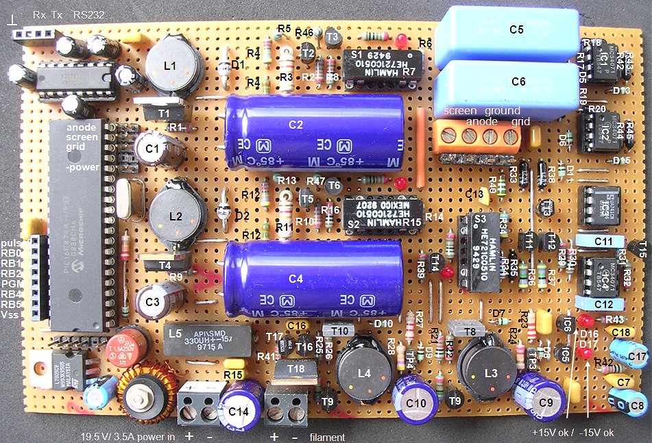
Figure 16.3 The floor plan of the uTracer.
The mysterious case of the erroneous AD converter.
During almost every project errors and problems are encountered which can give the unfortunate engineer gray hairs. Usually when I discover a problem and cannot find the solution straightaway, I take a step back, try to think of all the possible causes and examine these one-by-one. Sometimes this is effective, but most of the time it isn’t for the simple reason that if a problem is overlooked before, it is very likely that it will be overlooked again. What sometimes helps is to give the problem a good night rest. It has happened more than once that the solution to the problem suddenly pops-up in the morning in those mysterious moments
 during being a sleep and being awake. When even that doesn’t help and the problem persists, the situation becomes more problematic. Sometimes one arrives at the point when everything has been tried, and the problem seems to defy both logic as well as physics.
This story starts at the point when both the anode and screen boost converters where ready and being tested. At first sight they worked pretty fine. After entering a value, or indeed a series of values on the Graphical User Interface, the hardware promptly responded by adjusting the output voltage of the respective boost converter. However, there was a small error between the set point value and the actual voltage measured. A set point value of e.g. 200 V resulted in a measured value of 180 V. At first sight such a difference seems to be one of those obvious discrepancies between theory and practice, something that could easily be fixed by tuning some proportionality constant in the software. Nevertheless the difference made me feel a bit uneasy because the only two causes for such a discrepancy could be an inaccuracy in the resistor values in the “anode high voltage divider,” or a rather large deviation in the 5 V power supply voltage which is also used as a reference for the AD converters. The 5 V power supply was ok, so that could not be the reason, and the resistors in the voltage divider were 0.1% type devices so at first sight they were also not suspected. What then could be the cause?
The first obvious thing was to check the resistor values. They measured exactly what they should be. At that point I reached a dead end and couldn’t think of any other solution. So just to try something, I disconnected the voltage divider from the rest of the circuit en connected it to my high voltage supply. With exactly 200 V on the input of the divider, the AD converter input pin on the PIC measured 2.75 V
 while it should have been 2.43 V! This would exactly explain the difference. So how could the voltage on the output of the voltage divider be higher than expected? After again checking the resistor values, I disconnected the external voltage clamp diode to Vdd. A leak in this diode could easily “pull-up” the voltage at the input pin of the PIC. It made no difference. This was just crazy! The resistors in the voltage divider were ok, but the division ratio was not! The only logical conclusion had to be that the processor itself “raised” the voltage on the input pin! And indeed, after removal of the processor from its socket, the division ratio was exactly what it should be. But how can an analog input raise the voltage?
After insertion of an uA meter in between the AD converter input pin and the voltage divider, I found that the analog AD input pin sourced a current of approximately 54 uA! A very strange situation indeed! Where did the current come from? The first idea that popped up was that obviously the processor must have been damaged at an earlier stage. Replacing the processor with a brand new one however gave exactly the same result. The only logical – but as it later turned out erroneous – conclusion had to be that the fault was somewhere in the software. I spent literally hours in studying the datasheet to find if I had overlooked some stupid small thing that
 would cause this strange behavior. When that didn’t yield anything I started inserting breakpoints in the program. A breakpoint in this case was nothing more than a small infinite loop that would practically stop any further execution of the program. After a lot of trial and error I found that the current on the AD input pin appeared when that channel was selected by setting the corresponding bits in the ADCON0 register. Instead of clearing things up, it had made me more desperate.
I had noticed that when the input pin was not connected to anything, the reading of the AD converter jumped to 3FF, full scale. Apparently the mysterious output current charged to pin to the maximum potential. For one reason or the other I decided to measure this potential and to my astonishment I found that it was about 5.5 V. But the supply voltage of the processor was only 5 V (I checked it). How on earth could the voltage on an input pin rise to 5.5 V? After puzzling a few moments on this question all the pieces fell into place in a fraction of a second. If the voltage didn’t come from the supply pin, it had to come from one of the other pins. But from which one? Well, at this point I was only testing the high voltage boost converters. The inverting converter for the negative power supply was not yet activated. This meant that the opamps in the current amplifier were only driven from a positive supply voltage, and thus were biased asymmetrically, resulting in a voltage of 15 V at the output. Although I had protected the analog inputs of the processor with clamp diodes to Vdd, it could well be that the voltage drop over these diodes could be sufficient to cause the strange behavior. And low and behold, when the opamps of the current amplifiers were removed from their sockets, the mysterious current was gone, and a set point of 200 V again resulted in an output voltage of exactly 200 V. Simply switching the negative power supply on was not enough to solve the problem. Also during the charging of the large buffer capacitors the output of the opamps can be pulled so low that the input of the AD converter is pulles significantly below Vss. Replacing the clamp diodes by Schottky diodes however solved to problem completely. In retrospect a simple and logical explanation, but it took me two whole days. It was what my good friend Sherlock Holmes in “The Story of the Red Headed League” would call: “a typical three pipe problem.”
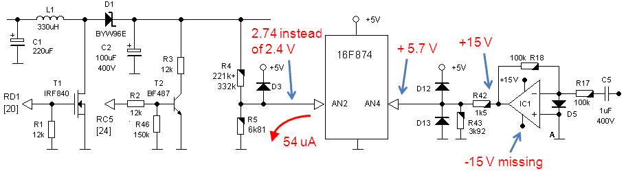
Figure 16.4 “A three pipe problem.”
| to top of page | back to homepage |
There are (at least) two reasons why the control part of the boost converters is implemented in software rather than in hardware. The first reason is that I wanted to make the uTracer really a minimum hardware device. The second reason is that it is rather a redundant step to use an DA converter to translate a setting point for the boost converter to the analog domain, while the whole thing could be done in the micro controller in the digital domain.
To understand how the software operates, it is good to first have a look at how a simple boost converter IC like the good old TL497 works. Figure 17.1A depicts a schematic circuit diagram of a boost converter using the TL497. The power part consisting of the inductor, power MOSFET, diode and buffer capacitor is rather standard and has been discussed at length in one of my other pages. The control part residing in the TL497 is very simple: a pulse generator generates the gate drive pulses which are gated to the MOSFET via an AND gate. The pulse width is chosen such that during the on-time (t_on), the current in the inductor doesn’t exceed the saturation current. The repetition frequency (1/T) is chosen such that during the off-time the current in the inductor completely returns to zero. A comparator compares the output voltage with a reference voltage, so that when the output voltage of the circuit drops below the pre-set value, the output of the comparator becomes “1” enabling the MOSFET to switch.
Figure 17.1 A “standard TL497 type” boost converter (left) compared to its software controlled equivalent (right).
There are obviously many ways in which such a boost converter control loop can be implemented in software. Fig. 17.1B depicts the implementation I have chosen. It is inspired by the fact that although the pulse repetition frequency is rather high (10kHz), the actual comparison of the output voltage to the set point can be performed at a much lower rate. The actual generation of the pulses is done by an interrupt service routine which is called every 100 us on the roll-over of one of the timers. The only thing the routine does is to check if a control flag is set, and if so to make the output that controls the gate of the MOSFET high. After a delay of 20 us the output is made low again and the routine returns to the main program. Note that nevertheless this routine “spoils” about 20% of the CPU time. The flag is set or reset by the main program. The main program selects the proper AD converter input, adds a delay for the sample and hold to settle, performs the AD conversion and compares the result with the preset value to either set of reset the flag. The control flag in this case acts as the AND gate in Fig. 17.1A. It is the means by which the main program communicates with the interrupt service routine.
This construction makes it very simple to control more than one boost converter. In the case of the uTracer for instance, four boost converters need to be controlled simultaneously. In this case there are four flags, and based on the status of these flags the respective outputs are made high or low during the same output pulse. In that sense adding more boost converters doesn’t add much to the CPU time. The main program one by one “polls” the output voltages and sets or resets the corresponding flags.
There is one small complication. In a normal boost converter, the boost converter circuit charges the buffer capacitor, while the load discharges it. However, the boost converters for the anode and screen have no load when the tube is switched off. So if we only have a simple “output is higher (or lower) than set point criterion” how can we know that the output voltage is correct and not way too high? Suppose for instance that during a previous measurement the anode buffer capacitor was charged to 300 V, and that for the next measurement it has to be 200 V. If we use a simple criterion like: the output voltage is ok if the output voltage is higher than the reference, it would result in a too high anode voltage. For this reason the software always first discharges the output buffer capacitor to a voltage below the set point before starting the charge it again. In this way we can be certain the output voltage is always correct.
Figure 17.2 Algorithm used in the uTracer to control the anode and screen boost converters.
The flow diagram depicted in Fig. 17.2 explains the algorithm used to control this process. Per boost converter three flags are used: the “pulse” flag which communicates with the interrupt service routine, the “D” or discharge flag which is high during the phase when the buffer capacitor is discharged, and the “ok” flag which becomes high as soon as the set point is reached. In reality the main program successively executes four of these algorithms, one for each boost converter. When the “ok” flags for all converters have become high, all the set points have been reached and the program continues by issuing the measurement pulse.
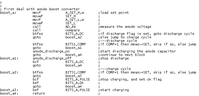
The example of the implementation of this algorithm is given in the piece of code above. In this case it is the code that deals with the anode voltage. The subroutine itself uses two other subroutines: “AD_AV” and “compare.” Routine “AD_AV” selects the proper analog input, delays for the sample and hold to stabilize, performs the AD conversion and stores the result amongst others in variables MEAS_L and MEAS_H. Routine “compare” compares the measured value to SET_H and SET_L. If MEAS >= SET then bit COMP in register BITS1 is set. The code for the screen converter is an exact copy of this one. The routines for the negative power supply and the negative grid bias are a bit simpler since there the discharge possibility has not been implemented.
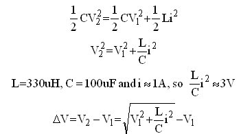
Figure 17.3 The voltage increment of the buffer capacitor after every conversion pulse can easily be calculated assuming energy conservation.
During every pulse of the boost converter, energy is stored in the inductor and then pumped into the buffer capacitor. The voltage increase of the buffer capacitor after a pulse can easily by calculated by assuming that after every pulse of the boost converter the energy stored in the inductor is added to the energy already stored in the buffer capacitor (Fig. 17.3). The voltage increase after a pulse of the boost converter obviously depends on the maximum current in the inductor and of the ratio L/C, but it also depends on the momentary voltage of the buffer capacitor. When the buffer capacitor is discharged, every pulse adds almost 3V. However, when the buffer capacitor is already charged to 200 V, each pulse only adds SQRT(300^2 + 3) – 300 = 5 mV.
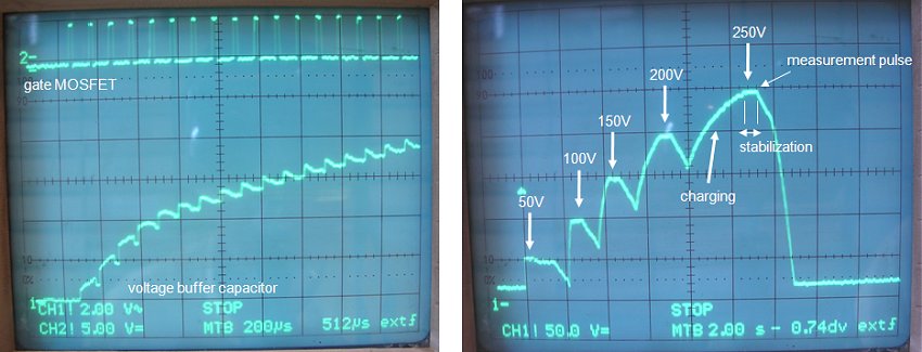
Figure 17.4 Two snapshots showing the charging of the anode buffer capacitor (see explanation below).
The charging of the buffer capacitor is illustrated in Fig. 17.4. The photographs in Fig. 17.4 were taken from the memory scope which was triggered by a special pulse added to the uTracer software in order to be able to capture these pictures. The left photograph in Fig. 17.4 shows the voltage of the buffercapacitor when it is charged from 30 to 40 volt. Note, that the increment in the voltage occurs immediately after each gate pulse. Also note the rather high discharge rate between each pulse. This is rather unexpected and something that I still have to look into. The right photograph is on a completely different time scale. It captures the voltage of the buffer capacitor when the uTracer goes through a complete measurement cycle and the anode voltage is stepped from 50 to 100, 150, 200 and finally 250 V. Observe that indeed for increasing voltages the slope of the charge rate decreases. When the set-point voltage is reached, the voltage stabilizes for ca. 0.7 s (flat plateau) at the end of which the measurement pulse is issued (not visible in this picture). After the measurement pulse the processor is busy sending and receiving data, so during this time the voltage drops. And again I am rather surprised by the high discharge rate (to be continued).
| to top of page | back to homepage |
Finally, after more than half a year of experiments and preparations the moment had come when the whole system could be tested. But first a few nasty errors and mistakes had to be corrected. There were one or two minor wiring errors on the PCB which were easily discovered, but a more serious mistake was that the inverting and non-inverting inputs of OpAmp IC3 had been exchanged in the original circuit diagram. Also in the original circuit diagram a diode was used to protect the input of IC3 in case of a flash-over in the tube. This diode, which never was tested, was another “fault pas” and has in the mean time been removed from circuit diagrams Figs. 10.1, 10.4 and 13.1.
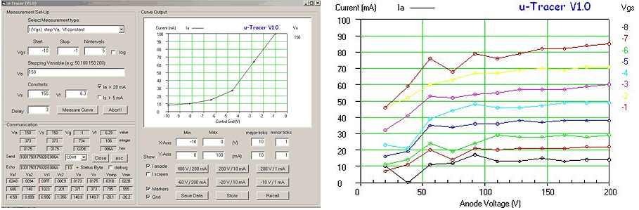
Figure 18.1 Left, a screen capture of the very first “curve trace” with the uTracer: a Ia(Vgk) curve of an EL84. Right, a set of Ia(Va) curves for the same tube.
Finally, in the weekend of 16/17 July 2011 the first curves with the uTracer were recorded. Figure 18.2 (left) is a screen capture of the very first Ia(Vg) curve measured on an EL84. With a shape as more or less anticipated, and with current values in the range where one would expecrt them, I was already euphoric! My enthusiasm got a bit tempered when I next tried to record a Ia(Va) set of curves (Fig. 18.2 right). The strange thing was that especially for the lower anode voltages the curves became very noisy. Immediately the boost converters in combination with the voltage dropper capacitors in the current sense circuits were suspected. And indeed after a few experiments my suspicions turned out to be right. What happens is rather complicated to describe, but I will have a go at it.
As already explained at the end of the previous section, the voltage increment of the buffer capacitor after each “boost pulse” depends heavily on the voltage of the capacitor. For low voltages the increment can be in the order of a volt or more, while for higher voltages the increment will be in the tens of mill volt range. Additionally the control loop which controls the firing of the boost pulses by the interrupt service routine is rather slow, so that usually once the control loop has set the “pulse” flag, ca. 4-5 pulses are fired before the voltage on the boost converter is evaluated again. This may cause small overshoots in the anode and screen voltages. The resulting “un-certainty” in the voltages is not such a big deal; an unaccuracy of a volt or so will be difficult to notice on a scale of 0 – 200 V. What is more serious is that the boost charging pulses also induce a current in the dropper capacitors of the current sense circuits. In the original firmware used to record Fig. 18.1, the measurement pulse was issued immediately after the moment when all the target settings were reached. In that way the time elapsed between the last (set) of boost pulses and the measurement pulse was unknown, resulting in an unpredictable offset in the current measured, especially for the lower anode (and screen) voltages.
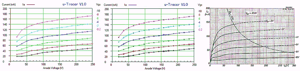
Figure 18.2
Long as this explanation is, the solution - or better let’s call it the bug fix - was simple. As soon as the target values for the voltages are reached, the boost converters for the anode and the screen are switched off for ca. 0.5 s allowing the buffer capacitors to charge. With this small modification of the firmware the rather nice curves shown in Fig. 18.2 were recorded. The left picture in Fig. 18.2 shows a set of Ia(Va) curves taken from an EL84 taken under the same bias conditions as the set of curves in the datasheet (Fig. 18.2 right). In the middle picture the “Store and Recall” function was used to compare two consecutive measurements. As can be seen the measurements are more or less identical, indicating a good reproducibility of the measurements.
The only thing that I was not so pleased with was the rather high output conductance of the tube compared to the datasheet. The root cause of the problem appeared to be a rather high discharge current during the stabilization phase immediately prior to the measurement pulse. The discharge current causes a drop of voltage of the buffer capacitor which appears as a positive offset on the output of the OpAmps which measure the anode and screen currents. The discharge current itself appeared to be partly caused by the tube itself, and partly by the measurement circuit. Remember that for grid biases between -15 and 0 V the grid is pulsed between -15 V and the specified grid voltage. It appeared however that for a grid voltage of -15 V an EL84 is not completely cut off. This is rather tricky because the tube is now sinking current during the charging of the buffer capacitors and there is no way of knowing this! However, even when the tube was removed from its socket, a current was measured which increased more or less linear from almost zero for Va = 0 V to ca. 12 mA for Va = 200 V. This current seems to be caused by the high voltage divider and the self-discharge current of the capacitors themselves. The simplest solution was to also measure the anode and screen currents directly before the measurement pulse. These values are then used to remove the offset from the real current measurements.
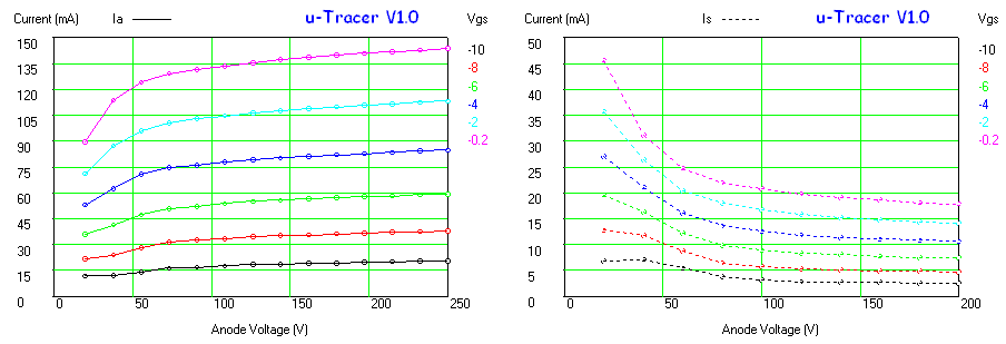
Figure 18.3 Anode current (left) and screen current (right) versus anode voltage for an EL84 measured with the uTracer (Vs = 200V).
Figure 18.3 shows the very first measurement taken with the offset correction in place (Thu. 21-07-2011). They are a nearly perfect set of output curves of an EL84 (compare them to the datasheet curves in Fig. 18.2). The next day the moment had come to finally realize what had been my ambition from the start of the project way back in January: to reproduce the measurements on an ECL80 which illustrated the original
1951 Philips Technical Review paper by Dammers et al. (see Section 3) [3].
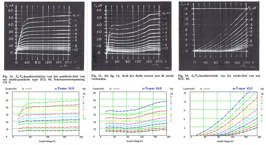
Figure 18.4 Output curves of an ECL80 tube copied from the original 1951 article [3] compared to identical measurements made with the uTracer (see explanation below).
The top row pictures in Fig. 18.4 is copied from the 1951 article from Dammers. The bottom row pictures is a set of output curves measured under identical conditions with the uTracer. The left column shows the pentode section of the ECL80 with the 3rd grid connected to the cathode. In the center column of pictures the pentode has been switched as a semi tetrode by connecting the 3rd grid to the anode. The right column finally shows the output characteristics of the triode section of the ECL80.
These measurements as well as those shown in Fig. 18.3 prove that the uTracer concept indeed works. Although this is, in its present state, not the most accurate tube measurement tool available, I have seen much worse. For a total construction cost of ca. 50 euro or so, it is indeed possible to build a tube curve-tracer not much larger than the size of a post card that can characterize even really heavy duty output tubes with reasonable accuracy. As expected I have also learnt a lot, lets’ try to make a summary of some of the findings:
At this point I also have a question to the readers of this page. What do you think? Is it worthwhile to develop an improved version 3.0? What features would you like to be added? What are you comments? Somewhere at the back of my mind I am also playing with the idea to design a professional PCB for this project and to sell it as a kit. Are you interested? Do you think other people will be interested? Please let me know by mailing me at:

For now there are a few things on my to-do list:
| to top of page | back to homepage |

Christmas 2010

This photograph has absolutely nothing to do with the uTracer. However, when I was working on this page, I went through a rather difficult period in my life because my wife was taken ill. In the middle of this period I also happened to become fifty. I hadn’t planned on celebrating my birthday, but my students decided to cheer me up by decorating my office, and they succeeded! I am very lucky to be able to work with such a group of great people! From left to right: Saeed Pakazad, Ting Yan, Aakriti Sing, Aashini Gulati, Adnan Noor, and Angel Savov. Date: 8th June 1911.