
This page originally contained the circuit description of the uTracer3. Now that the uTracer3 has been succeeded by the uTracerNXT, the content of the page has been adapted accordingly. The original description of the uTracer3 circuit can still be found here. Writing a concise description if the uTracer6 circuit is on my list of things to do, but since the uTracer6 and uTracerNXT have many elements in common, the description of the uTracerNXT below will also give a good idea of the working of the uTracer6. For all uTracers extensive background information can be found in the respective Weblogs.
At first sight the circuit diagram of the uTracer may seem rather intimidating. It is true that there are quite a few components, but most of them are standard components like OpAmps, resistors, capacitors and transistors. Furthermore, the circuit consists of a number of blocks which to a large extend operate independently, and what is more, can be tested in dependently. On this page these blocks will be discussed in some detail. To keep the explanation comprehensible many details will be skipped. These details can be found in the project blog of the uTracerNXT. For the convenience of the readers a large number of links are included which directly point to the relevant part in the project blog text.
My-uTracer
A new aspect of the uTracerNXT is that it is possible to “personalize” the measurement ranges to optimize the ranges versus resolution trade-off to one’s specific needs. The default voltage and current ranges of the uTracerNXT after construction are:
- Anode/Screen voltages 2 – 500 V
- Anode/Screen currents 0 – 350 mA (0 – 250 mA with compliance switched on)
- Control Grid voltage 0 – 120 V
These ranges are a compromise to accommodate the tracing and measurement of a wide variety of tubes. However, sometimes it may be desirable to modify these ranges e.g. to allow higher currents, or to measure battery tubes at low voltages etc. The uTracerNXT has been designed so that it is relatively easy to modify the default ranges, and to switch back and forth between the standard and the personalized configuration.
Modifying the ranges is done by adding a resistor in parallel to a “fixed” default resistor that was installed during the construction of the kit. At first sight this may seem an odd way of changing resistance values! Why not simply switch between two resistors? The reason is that in this way a situation may occur where there is no resistor connected at all! Since this might result in a dangerous situation, we use the “parallel resistor” method to ensure that there is always a resistor in place. The project blog contains a detailed description of how the ranges can be modified. On the PCB the modified range can be “activated” by placing a jumper
(more).
Ihor Small as thought of a brilliant way to make these jumpers easily accessible
(more).
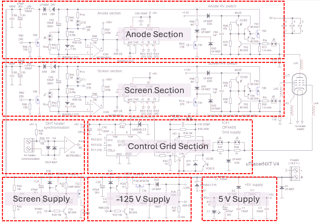
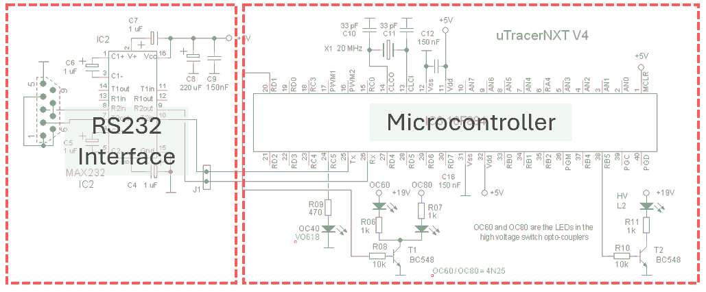
Figure 1. Building blocks of the uTracerNXT tube tester. The complete circuit can be found at the bottom of this page.
Microcontroller and Interface
The heart of the uTracer is a 16F884 PIC micro-controller from MicroChip. The controller is used in a standard configuration with a 20 MHz external X-tal. Like in the older two uTracers, I have still chosen for a 40 pin DIL package in a socket. Experience has learned that this is the easiest way to allow for easy circuit debugging and if needed repair.
Many people have commented about the “old fashioned” RS232 interface. A true native USB interface is complicated to implement by amateurs and even (semi-) professional organizations. A lot of even professional equipment with a USB interface use a chip from FDTI to convert USB to serial so that it at least from the outside looks as if it has a USB interface, but in reality, it will still generate a virtual COM port. Since FDTI chips only come in difficult high pin count SMD packages, I have chosen for a standard well defined RS232 interface. Many people have an RS232 to USB converter lying around, or otherwise they can be purchased for a few bucks.
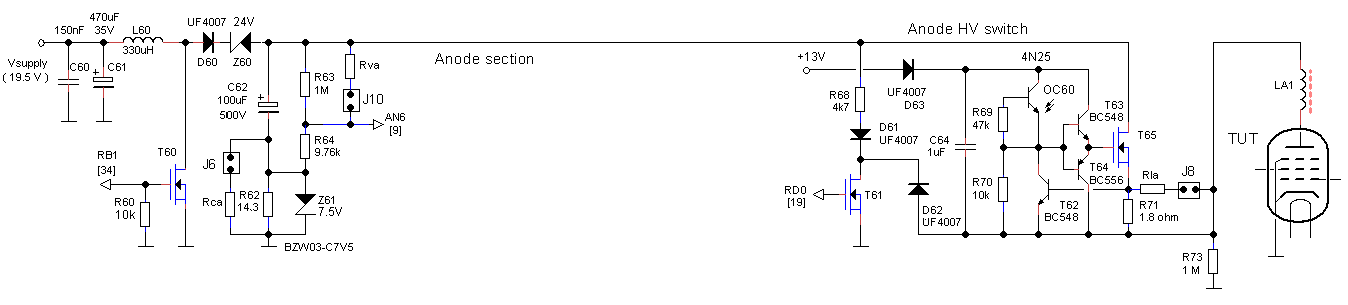
Figure 2. Detail of the anode supply circuit showing the boost converter on the left and the high voltage switch on the right.
Anode and Screen Supplies
The anode and screen supplies consist of two identical circuits. As explained on the previous page, the uTracers work in a pulsed mode, meaning that the voltages are only applied to the tube for half a millisecond during which the currents are measured. Each supply consists of three sub-blocks: a boost converter which charges a large 100 uF capacitor to the desired test voltage, a floating high voltage switch which briefly connects the capacitor to the anode or screen of the tube, and a means to measure the current.
An important difference of the uTracerNXT compared to its predecessors is that the cathode of the tube is connected to ground instead of the positive supply voltage. The main reason why the cathode was connected to the positive supply voltage is that in a normal configuration the minimum output voltage of a boost converter is the supply voltage. In the uTracerNXT Zener diode Z60 (Fig. 2) is used to “remove” the supply voltage on the output side of the boost converter (more). Having the cathode of the tube connected to ground reduces the complexity of the control grid bias circuit and makes more sense anyway.
During charging of C62 zener diode Z61 is in forward mode and conducting so that the voltage building up on C62 can be monitored by the microcontroller through voltage divider R63 R64, which is dimensioned in such a way that the maximum voltage of 500 V is reduced to 5 V. The voltage range can be reduced by adding resistor Rva parallel to R63. This will increase the resolution and accuracy at lower voltages e.g. enabling the testing of battery tubes (more).
The high-voltage switch, shown on the right side of Fig. 2, is nearly identical to the switch developed for the uTracer6. The circuit was discussed at length in the uTracer6 weblog (more). The heart of the switch is high-voltage MOSFET T65. The gate of T65 is driven by push-pull buffer T63 & T64. The buffer has a high impedance input and a low impedance output and avoids dV/dt issues (more). A simple circuit consisting of T62 & R71 provides the hardware current protection. When the voltage over R71 exceeds approximately 0.7 V, T62 starts to conduct thereby limiting any further increase in current. Note that in normal operation the power dissipation in T65 is negligible. However, when the hardware current limit is activated, T65 will absorb as much voltage as needed to limit the current. Worst-case in case of a full short circuit at the output this can be the full output voltage. In this situation T65 will dissipate a huge amount of power. There is therefore also a software overcurrent protection that switches the current off as quickly as possible (more).
Remember, that during operation, the switch circuit needs to be floating with respect to ground so that all the anode current also flows through current sense resistor R62. The high-voltage switch is therefore controlled by the PIC processor through opto-coupler OC60. Immediately before a measurement pulse, T61 is briefly switched on so that C64 through D62 & D63 is charged to 13 V. The charge stored in C64 is enough to power the high-voltage switch during the subsequent measurement pulse.
The second function of T61 is to discharge reservoir capacitor C62 at the end of a measurement cycle. Note that during the measurement pulse itself, T61 is not conducting so that the high-voltage voltage switch is indeed electrically floating.
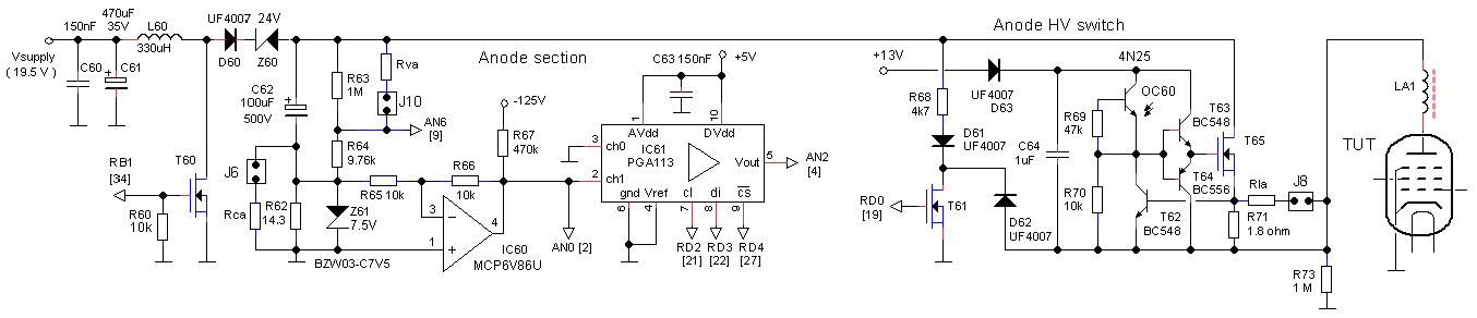
Figure 3. The complete anode supply circuit, which is identical to the screen supply circuit.
As mentioned, the anode current is measured by measuring the voltage drop over current sense resistor R62. In a 5 V system, the 14.3 ohm current sense resistor results in a maximum current of 5/14.3 = 350 mA. In the my-uTracer concept the maximum current can be increased by adding a resistor in parallel to R62. (more). If se desired, the current accuracy and resolution can also be increased by decreasing the maximum current range (more).
Note that the voltage drop across the current sense resistor is negative with respect to ground. It is therefore inverted by OpAmp IC60 which is used as a -1X gain inverting amplifier. The MCP6V86 is a high-performance affordable OpAmp designed for single supply 5 V operation. Although these modern OpAmps are advertised as rail-to-rail, they actually never can reach exactly 0 V output voltage. The quiescent current through the output stage of the OpAmp always causes a (small) voltage drop over the inevitable on-resistance of the low-side output transistor. Fortunately, in some cases when a negative power supply is available, a simple trick can be used to really pull the output to 0V. Resistor R67 connects the -125 V negative power supply with the output of the OpAmp. It has been dimensioned in such a way that it is more or lessequal to the quiescent current in the output stage of the OpAmp. Since the low-side output transistor is now more or less current less, the output voltage can really drop to practically zero (more).
Zener diode Z61 has a double role. Apart from conducting in forward mode during the charging of C62, it acts as a protection during an overload condition. During a short circuit at the output of the anode supply, the (negative) voltage over the current sense resistor would increase sharply, but is clamped to 7.5 V by Z61, which is now in reverse mode. Together with R65 this protects the OpAmp from damage.
The output signal of the OpAmp is now a 0 to +5V signal proportional to the anode current. This is fed into the input of IC61. This is a Programmable Gain Amplifier (PGA). Under software control the gain of the PGA can be set to 1,2,5,10,20,50,100, and 200; a set of gains which is sometimes also called “a scope range” (more). As mentioned, the gain is set under software control whereby the user has two options: 1. Select a gain manually, 2. Use an auto-gain algorithm so that always the most optimal gain is selected (more).
Additionally, the input signal of the PGA, basically the inverted voltage drop over the current sense resistor, is connected to one of the analog inputs of the controller. It is a part of the second defense line against short circuits. In the micro controller the signal is compared to the output voltage of an internal programmable voltage reference. When the voltage drop over the current sense resistor exceeds a certain pre-programmed value an interrupt is generated which immediately switches off the high-voltage supplies. In practice this means that the high voltage is switched off within 20 us after an over current situation has been detected. To summarize what happens during a short circuit: first the current is limited by the hardware circuit around T62 and R71. This limits the current, but can still causes excessive peak dissipation in T62 even though the measurement pulse only lasts 0.5 millisecond. So 20 us after a short circuit is detected by the controller, the high-voltage switch is opened to limit the total amount of dissipation. Despite these precautions, care should be taken to avoid a short circuit since this is at any rate a very violent event which stretches the circuit to its limits (more).
The Grid Supply
The grid bias supply is relatively straight forward. In the default configuration, the grid bias supply generates a programmable voltage between 0 and -120 V. The grid bias supply is controlled by a 12 bit DAC, in principle resulting in a 120/4096 = 29 mV resolution. The MCP4921 DAC is provided with an 2.5 V LM4040-2.5 external voltage reference source.
The output signal of the DAC is amplified and inverted by an OPA455 high-voltage OpAmp. The total maximum differential supply voltage of the OPA455 is specified as 150 V. In this circuit the OpAmp is fed from a high asymmetrical power supply voltage of +5 V and -125 V. Even though in normal use the output of the OpAmp hardly needs to deliver any current, I still choose to operate it in pulse mode to limit the dissipation should there be a fault either in the tube or in the connections to the tube. Conveniently, the OpAmp has an enable input. Because of the highly asymmetrical power supply, operating the enable input is a bit tricky and solved using opto-coupler OC40
(more).
When jumper J3 is removed, the pulse mode operation is disabled to facilitate calibration of the grid supply. In normal use however, I strongly recommend placing jumper J3.
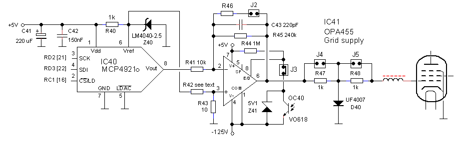
Figure 4. The Grid Bias Circuit of the uTracer tube tester.
At the output of the OpAmp R47, R48 and D40 protect the OpAmp against short circuits and flash-overs. During a positive flash-over, diode D40 conducts while R48 limits the current through the diode. At the same time R47 limits the output current of the OpAmp. Although normally the grid current drawn by a tube, and hence the voltage drop over R47 and R48, is negligible, for grid voltages very close the zero, a small grid current will start to flow. In those cases where this could could result in a significant measurement error, jumpers J4 and J5 can be placed to bypass the protection circuit. However, in normal operation I recommend to remove J4 and J5.
In the default configuration the amplification of the OpAmp is set to 240/10 = 24x. However, by adding a resistor in parallel to feedback resistor R45 the gain of the OpAmp can be lowered. This reduces the maximum grid voltage range, but proportionally increases the resolution (more). I can imagine that many users will default set the grid bias range to e.g. 0 to -50 V and only use the full range for the testing of “heavy” output tubes.
A circuit like this inevitably exhibits some offset. Although the datasheet of the OPA455 specifies a typical input offset of +/- 0.2 mV, the maximum offset voltage we must consider is +/- 3.4 mV. With a gain of 24x this can result in an output offset of +/- 84 mV, and this is even without considering the offset of the DAC. It is very simple to correct for positive offset voltages (measured at the output) in software. However, this is not directly possible when the total offset voltage is negative. In case the total offset voltage is negative, it is first made slightly positive by adding a tiny bias to the positive input of the OpAmp by means of R42 and R43. The positive offset if then again compensated for in software (more). The procedure sounds a bit cumbersome, but in practice works quite well and is step-by-step explained in the construction manual. I could have opted for a 10-turn trimmer potentiometer, but I rather dislike them. They are expensive, noisy and always tend to be out of stock.
The Heater Supply
Much has been written and said about the heater supply of the uTracers. There are so many very good, and extremely cheap (Chinese) power supplies available online that in all fairness no “homebrew” solution can compete with those (more). However, I nevertheless wanted to include a simple heater supply to come to a self-contained single board tester that will get people started and is good enough for most practical measurements. If so desired, an external heater supply can easily be included as can be seen in the many uTracer embodiments found on the testimonial page(s) (more).
The heater supply circuit is very simple (Fig. 5). Since the heater of a tube is basically nothing more than a resistive load, a simple Pulse Width Modulation (PWM) circuit can be used to control the amount of dissipated power. Heaters, especially heaters of power tubes, consume a lot of power. An EL34, a popular audio output pentode, dissipates about 1.5 Amp at 6.3 V. An (old) laptop power supply that I recommend as power supply for the uTracer can supply a lot of power, usually many tens of watts. The output voltage is usually 19.5 V. Since the heater voltage is directly derived from the power supply it is important to know the exact value. That is why the uTracer measures the supply voltage immediately after start-up through voltage divider R02 and R03. Obviously, the maximum heater voltage is limited to the power supply voltage. When a higher heater voltage is required an external power supply must be used.
The PWM signal is generated by one of the PWM generators on board of the microcontroller. Note that since we need to regulate the power delivered to the heater rather than the average voltage, the PWM duty cycle is proportional to the square of the heater voltage!
(more).
In the uTracer3 a PWM repetition frequency of 19.5 kHz was used. It appeared that this rather high frequency in combination with parasitic inductances in the heater leads resulted in “losses” so that the actual power to the heater was less than expected, especially for tubes with a “heavy” heater. In the uTracer6 and uTracerNXT this problem was solved using a much lower PWM frequency of 1.2 kHz. The only disadvantage is that now a soft 1.2 kHz sound is audible
(more).
Note that during the actual measurement pulse the heater supply is switched of to reduce noise in the circuit and allow for actual measurements.
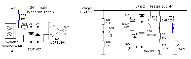
Figure 5. The heater supply consists of two sub-blocks. On the left the AC synchronization circuit and on the right the heater supply itself.
In contrast the uTracer3 and uTracer6, in the uTracerNXT the cathode is referenced to ground. To allow for the measurement of directly heated tubes, this implies that in the uTracerNXT also the heater must be referenced to ground. This necessitates the use of a PMOS transistor to drive the heater. To drive this PMOS transistor normally transistor T21 and resistors R21 and R22 would have sufficed. It was found however, that as a result of the relatively high gate capacitance of PMOS transistors compared to NMOS transistors with a comparable current/Ron rating, the switch-off time of the PMOS transistor was rather slow, resulting in a too high power delivered to the heater, especially for low voltage heaters. The problem was solved by a simple bootstrap circuit consisting of C21, D21 and T23 which actively removes the charge from the gate of T21 at the trailing edge of the PWM signal. (more).
High power transmitter tubes often employ a directly heated cathode that draws many amps of current at a few volts. In a transmitter these heaters are usually directly powered by an AC transformer. Without special precautions, tracing of directly heated tubes that are powered by an AC source will result in “noisy” curves since the moment of the 0.5 ms measurement pulse occurs at a random moment with respect to the AC cycle, resulting in an arbitrary fluctuation of the effective grid-cathode voltage. For the uTracer6 an option was developed that synchronizes the measurement pulse with an external AC source (more).
The circuit worked so nicely that it was decided to make it a standard part of the uTracerNXT. The heart of the synchronization circuits is OpAmp IC4 which is used as a comparator. Diodes D3 and D4 together with R4 limit the input voltage to the OpAmp to +/- 0.7 V. R5 prevents arbitrary toggling of the output of the OpAmp in case no AC source is connected. The output of the 5 V single supply MCP6V86 OpAmp can directly interface with the microcontroller (more). The construction manual describes in detail the different options how an AC/DC heater supply can be connected to the uTracerNXT. (more).
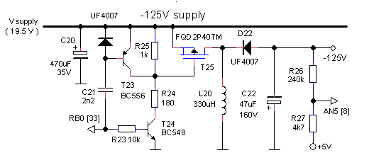
Figure 6. The Negative Power Supply.
The -125 V Negative Power Supply
The last and least interesting circuit block left to discuss is the -125 V negative power supply. It provides the negative voltage for the grid supply and for the “trick” to make the outputs of IC60 and IC80 truly go to ground. The circuit is a standard inverting boost converter which is like the high voltage boost converters fully controlled by the microcontroller. Voltage divider R26 and R27 is dimensioned such that at an output voltage of -125 V the feedback voltage to the microcontroller is approximately +2.5 V. Identical to the heater supply a bootstrap circuit consisting of D21, C21 and T23 is used to improve the switch-off time and hence the power dissipation of T25.
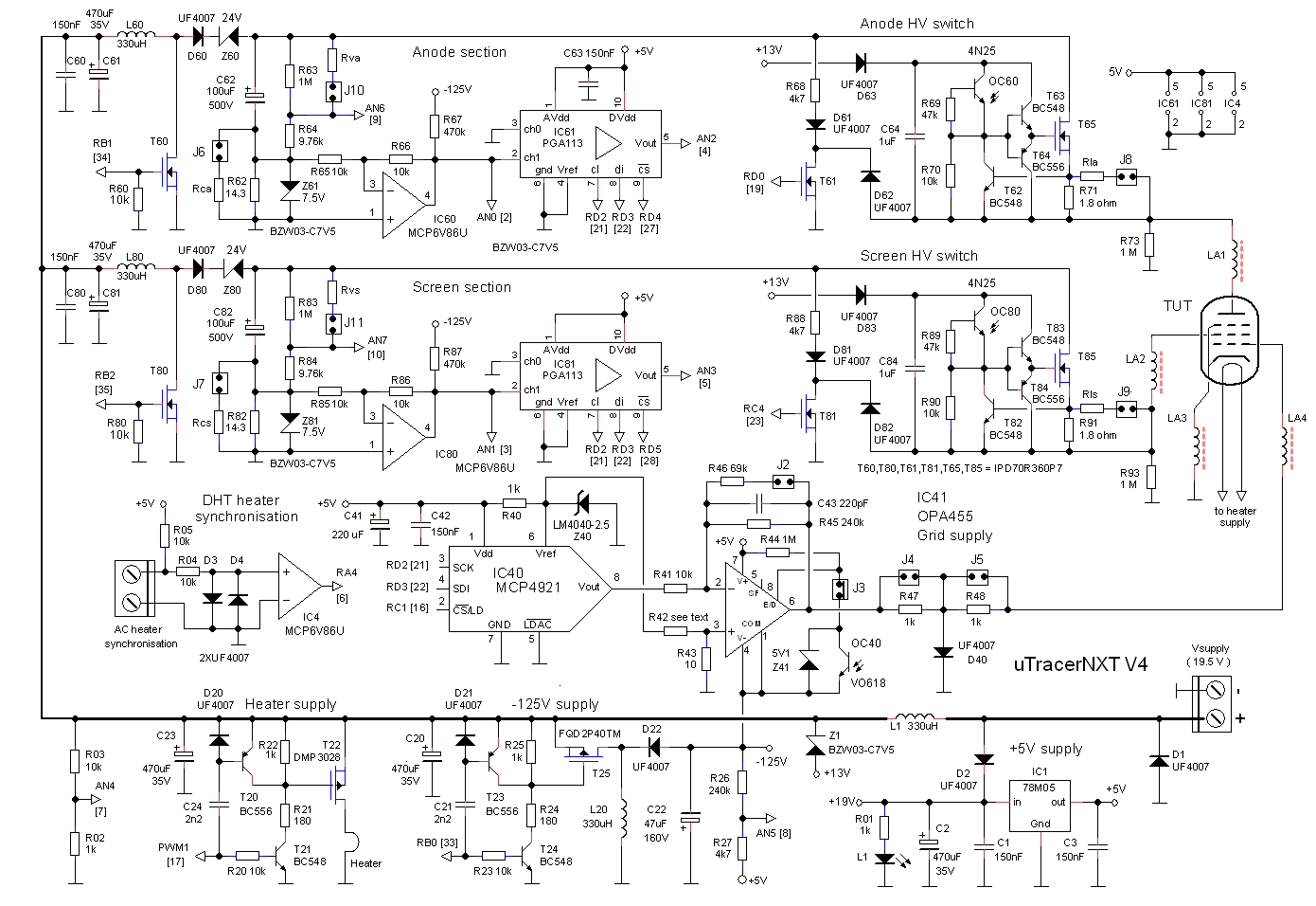
Figure 7. Total circuit of the uTracer V3.
| previous page | next page |

Cartoon bij Hans Evers PAoCX