Surfing the web searching for exotic clocks, I came across
the fantastic clock made by Pieter-Tjerk de Boer from Holland [1]. This amazing clock uses only neon light-bulb as logic elements (Fig. 1). The neon light-bulbs are used in so called ring counters. Pieter-Tjerk’s facination for neon ring counters was aroused by the book “Electronic Counting Circuits” by J.B. Dance [2] which was discarded by the liberary of the Technical University of Twente. Fortunately the liberary of the Technical University of Delft still holds a copy of Dance’s book. It is indeed a fantastic and exhaustive treatment on all kind of counting circuits known in 1967. Recently I discovered that the complete book is available for downloading on Dieter’s “Nixie World” site. Klick here, to download a zip archive with the complete book from his site (36Mb!). Thanks Dieter!
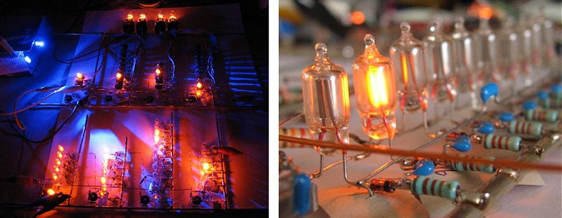
Figure 1. A nixie clock based on neon tube ring counters made by the Dutch radio amateur
Pieter-Tjerk de Boer (PA3FWM). Click here or on the picture to few his fantastic project.
Chapter 3 (Single Cathode Gas filled Counting Tubes And Their Circuits) contains a section titled “Simple Cold Cathode Tubes”. It explains the working of the neon ring counter, and I have to admit that I had never heard of neon ring counters. They turn out to be very fascinating simple circuits. Their working is based on the fact that these tubes exhibit a hysteresis in their on- and off-switching. Imagine that a potential is applied to a neon tube that lies between the extinguishing voltage and the striking voltage. The tube can now be switched on by applying a short pulse that raises the potential over the tube above its striking voltage. Similarly the tube can be switched off by a short pulse that lowers the potential below the extinguishing voltage. The neon tube is therefore equivalent to a logic circuit element with a memory. In datasheets these tubes are therefore often referred to as “Switching Diodes.”
Figure 2. Two illustrations from the November 1966 number of Electronics Illustrated which featured a
Digital circuits that used these neon tubes have only been popular for a relatively very short time, say between 1950 and 1970. On one hand digital circuits only became popular after the war, while on the other hand the invention and development of the transistor quickly made these neon switching tubes obsolete. In 1958 “Electronics” published an article entitled “Elementary Computer acts as silent adversary to a human opponent in an ancient pastime” [19]. The article described a circuit in which Thyratrons, relais and digital neon gates were used to construct a machine that could play “Tick-Tack_Toe.” Eight year later these digital neon circuits were apparently still popular, since “Electronics Illustrated” of November 1966 featured an extensive project which described an electronic calculator based on neon-tube ring counters (Fig. 2) [4]. Although it was a crude and clumsy machine that used a telephone dial as input, it was announced as “a Space-Age Decimal Computer”. All in all I found that these tubes and circuits were fascinating enough to make a little study out of them and to see if I could built a clock based on ring counters myself. Rather than first finishing the complete project and then write a complete page on it, I decided - just as with my decatron clock project - to write this page in a weblog form, so that I will add chapters as the project progresses. So check this page out from time to time if you are interested in neon ring counters.
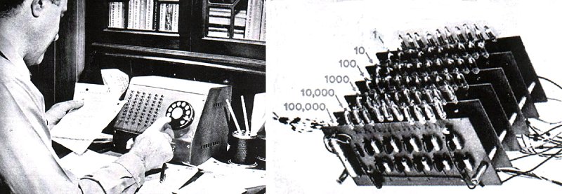
“Space-Age Decimal Computer” [4]. Click here or on the picture to download the full article. Have a look at this great site by Albertus Bredekamp who actually built this neon calculator!
| to top of page | back to homepage |
The neon ring counter circuit was originally proposed by John Manley and Elery Buckley from MIT. In their paper ”Neon Ring Counter” in Electronics, January 1950, they discussed a three-decade ring counter constructed entirely from neon tubes and germanium diodes, capable of incrementing, decrementing, reset and preset. The counter would count up to 30.000 impulses per second (Fig. 2a). Reliable germanium diodes were very new and advanced components in 1950 (The first press announcement of a germanium diode in Holland was in 1946). Looking at the circuit diagram in Fig2a, we see that the ring counter circuit was arranged in a slightly different way than we are used to today. Note also that the circuit symbol for a diode had not yet evolved to the symbol we use today, but actually still very much resembled the construction of a point contact diode.
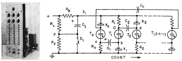
Figure 2a. Two illustrations from the January 1950 number of Electronics which show a picture of the original three-decade neon counter
proposed by manley and Buckley, and the circuit diagram of their basic counting cell.
Click here or on the picture to download the full article.
Logic circuits such as ring counters made with neon tubes are based on the fact that for a gas discharge tube such as a neon tube, the ignition voltage can be made higher than the extinguishing voltage. This peculiar behavior is illustrated in Fig. 3, where we find a neon tube connected via a current limiting series resistor connected to a variable voltage source. The fictitious neon tube in this example has a striking voltage (Vs) of 140V. The striking voltage is also referred to as the ignition voltage or firing voltage. The maintaining voltage (Vm), running, or extinguising voltage of the tube is assumed to be 100V.
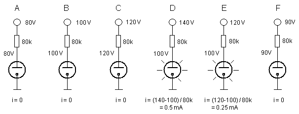
Figure 3. A simple neon tube circuit under different biasing conditions, explaining the consequences
of the difference in striking (Vs) and maintaining (Vm) voltages of a gas discharge tube.
In this example Vs=140V and Vm=100V
In Fig. 3A, the supply voltage has been increased from zero to 80V. Since this is still well below the striking voltage, the tube will not ignite and the current will be zero. Since there is no voltage drop over the series resistor at zero current, the voltage across the tube will be identical to the supply voltage. Next the supply voltage is slowly increased to 120V (Figs. 3B and C). Since this is still below the striking voltage, the tube will not strike. However, when the supply voltage is now raised to 140V, the tube ignites (Fig. 3D). Once ignited, the voltage across the tube will drop to the maintaining voltage of 100V and a current will start to flow. The current flowing through the tube is limited by the resistor and can be calculated from the supply voltage minus the maintaining voltage divided by the resistor value. Further increasing the supply voltage will linearly increase the current, since the voltage across the tube is basically clamped to Vm=100V. Alternatively, when the supply voltage is now reduced to say 120V - which is still above the maintaining voltage of 100V - (Fig. 3E) the current will be reduced but the tube will still remain ignited. Only when the supply voltage is finally reduced below the maintaining voltage, the tube will extinguish, and the current will return to zero (Fig. 3F).
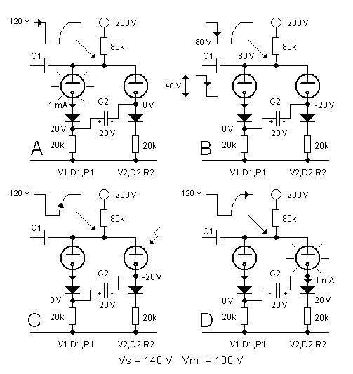
Figure 4. Two stage ring counter at different stages of its operation.
Equipped with this knowledge it is now easy to understand how a neon ring counter works. In Fig. 4 a two stage ring counter is depicted at different stages of its operation. The basic buiding block of the counter consists of a neon tube, a diode and a resistor in series, connected to the next stage by means of a capacitor. Lets assume that the neon tubes used in this example also have a striking voltage of 140V and a maintaining voltage of 100V. Lets furthermore assume that in the starting situation neon tube V1 is on, while V2 is off (Fig. 4A). Since V1 is on, the voltage across V1 will be its maintaining voltage of 100V. The remaining voltage will divide between R1 and the common anode resistor, resulting in a voltage drop across R1 of 20V. Since V2 is off, the voltage drop across R1 will be zero. As a result C2 will be charged to 20V as indicated in Fig. 4A. In this page I will call the voltage over C2 the cathode transfer bias.
Next, a negative going pulse with an amplitude of 40V is applied to C1, the input of the counter (Fig. 4B). This negative going edge will for a short moment (the voltage across a capacitor cannot change instantaneously) reduce the anode potential of both tubes to 80V. Since this is well below the maintaining voltage of 100V, V1 will extinguish. Both tubes are now off. Since there is now no current flowing in either branch the voltage drop across R1 will be zero. C1 however, was charged to 20V so that the cathode of V2 will be at a potential of -20V (the cathode transfer bias) with respect to ground. Note, that C2 will remain charged because D2 is blocking and V2 is off.
The anode potential will not remain at 80V, since the common anode resistor will start to charge C1 causing a potential rise of the common anodes (Fig. 4C). If nothing would happen this would cause the anode voltage eventually to increase to 200V. This will never happen because when the anode potential reaches 120V, the voltage across V2 (whose cathode was biased as -20V) reaches the striking voltage of 140V, and V2 strikes (Fig. 4D). The glow has now been transferred by a counting pulse from tube V1 to tube V2.
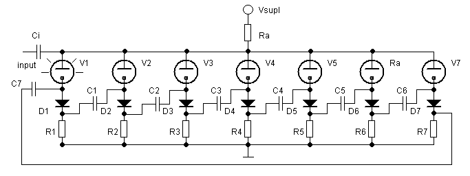
Figure 5. Example of a seven stage neon ring counter.
By cascadingany arbitrary number of sections, and feeding back the last section to the first section, a ring counter is obtained (Fig.5). A negative going pulse on the input that is large enough to reduce the voltage over the glowing tube below its maintaining voltage (Vm), will shift the glow to the next tube in the ring. If the pulse length is shorter than the deionization time, the tube will ignite again when the maintaining voltage is re-applied. The deionization time is normally in the order of some milliseconds. This limits the speed of cold cathode diode ring circuits to ca. 1kHz [2,p.41].
| to top of page | back to homepage |
In the previous section we have seen how the working of a neon ring counter relies on the fact that the maintaining voltage of a neon tube is significantly lower than the striking voltage. In an ideal world, where all neon tube would be exactly the same with zero process tolerances, only a few volts difference between the striking and maintaining voltage would be needed. However, in reality no tube will be the same, resulting in smaller and larger differences in striking and maintaining voltages. On top of that these voltages are likely to change over time due to aging. Intuitively we feel that preferably the difference between striking and maintaining voltage should be as large as possible, and that the cathode transfer bias should be approximately half the difference between the two. In the next few paragraphs we will try to come to some more scientific conclusions.
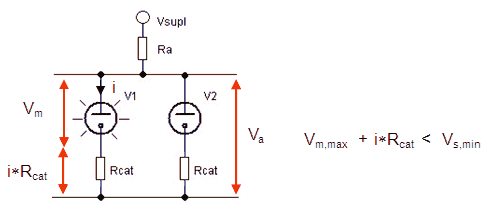
Figure 6. Simplified diagram of the basic ring counter.
Figure 6 shows a simplified circuit diagram of the basic ring counter section as depicted in Fig. 4. For simplicity the diodes and in capacitors have been omitted. We assume that V1 has ignited so that the voltage across V1 is the maintaining voltage. The current flowing through V1 causes a voltage drop over Rcat (the cathode transfer bias for the next section) of I*Rcat. The sum of Vm and I*Rcat should obviously be less than the striking voltage of V2.
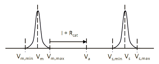
Figure 7. Graphical representation to derive the consequence of the process variations for the cathode transfer bias.
In Fig. 7 this is illustrated graphically. Additionally the tube to tube variations have been included by means of two semi-Gaussian distributions. The average value of the maintaining voltage e.g. is indicated by Vm, while the minimum and maximum maintaining voltages in a ring are represented by Vm,min and Vm,max respectively. It is now obvious that a worst-case situation occurs when V1 is a tube with the highest maintaining voltage of the ring Vm,max, while V2 is the tube with the lowest striking voltage Vs,min. To ensure proper operation even in this case, I*Rcat has to be smaller than Vs,min – Vm,max.
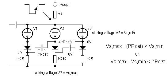
Figure 8. Circuit used to assess the lower bound value for I*Rcat
Whereas the previous analysis set the upper bound value for I*Rcat, the circuit of Fig. 8 can be used to derive the lower bound value. It depicts a three stage ring counter at the stage where V1 just has been extinguished by a negative pulse on the common anode node, so that the capacitor has been charged to the cathode transfer bias I*Rcat. The anode voltage is just rising again so that V2 should strike first.
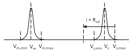
Figure 9. Graphical presentation to derive to derive the lower bound value of the cathode transfer voltage
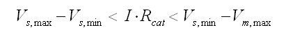
In the circuit of Fig. 8 a worse-case situation occurs when neon tube V2 has the highest striking voltage of the ring. When the difference between the striking voltage of this tube, and the minimum striking voltage in the ring is less than I*Rcat, the latter tube will strike instead of V2. In other words: Vs,max - Vs,min < I*Rcat (Fig. 9). This condition sets a lower bound value for I*Rcat. So summarizing we have found:


After all this thinking, the correct procedure to establish the component values in a ring counter now becomes a bit clearer. If you have enough tubes, it is a good idea to first sort them in such a way that you end up with ten tubes with minimal variations in Vm and Vs. The best approach now is to average I*Rcat between the lower and upper bound values we have derived. The datasheet of the tube gives us the nominal current (usually something in the order of 1 mA). We can now calculate Rcat from:


| to top of page | back to homepage |
Neon tubes, or switching diodes as they are sometimes called come in two flavours: tubes with barium coated cathodes and tubes with sputtered metal cathodes (see also section The ZA100X series switching tubes from Philips). To understand why cathodes need to be prepared either way, we have to understand that due to residual oxygen molecules in the gas of the tube, the cathode always will be covered with a monolayer of oxide. This layer has a very high work function, meaning that it will cost a large amount of energy to free an electron from the surface of the cathode. Now when a small amount of material with a very low function like barium or cesium is deposited on this oxide layer, the low work function material will exchange an electron with the oxygen, resulting in the formation of a dipole layer. The dipole layer will effectively lower the working function of the cathode to a very low value.
The vast majority of all neon tubes use a barium-coated cathode. Barium-coated cathodes have two advantages. First of all, metal cathodes have to be cleaned – in situ - by sputtering. During the sputtering of the cathode also a non transparent metal film will be deposited on the tube envelope so that the glow will only be visible at the ends of the tube where less material is deposited [3]. The second advantage is that due to the low work function of the barium coating, normal visible light can be used to photo-electrically primer the tube. This probably needs a bit of explaining. For a reliable striking of a neon tube, a certain number of ions need to be present. A few ions per minute are formed in the tube by cosmic rays and by radiation from stray radioactive atoms which are present in all materials, but more ions are needed if the discharge must always be initiated rapidly [2]. Artificial methods for increasing the number of ions in cold cathode tubes are known as priming. Apart from photo-electrical priming, also sometimes an additional priming electrode is used, or a little radioactive tritium gas is added to the gas mixture, to ensure reliable and rapid striking of barium coated tubes even in the dark.
The vast majority of neon tubes, especially the ones that are on the market today, have not been designed for switching applications. Consequently, in designing these tubes no effort was made to maximize the difference between the striking and maintaining voltages. Typically, these neon tubes have a striking voltage of approximately 80V and a maintaining voltage in the order of 60V. On top of that these parameters tend to show a rather large variation from tube to tube, due to mechanical tolerances in their constructions and variations in the barium coating process and the gas mixture and pressure. All in all the application of ordinary neon tubes for switching applications tends to result in critical circuits which require low tolerance components.
Figure 10. A Circuit used to age the neon tubes, B test circuit to measure Vs and Vm.
One way to deal with this is “to bin” the tubes prior to use. This means that both Vs and Vm are measured for each individual device, and that they are then “binned” into groups with more or less similar characteristics. Both Pieter-Tjerk de Boer with his ring counter clock [1], as well as the authors of the ring counter calculator in “Electronics Illustrated” [4] follow this approach. Since the characteristics of the tubes tend to shift when they are first switched on, it is advisable “to age” the tubes prior to binning. In “Electronics Illustrated” a procedure is proposed to age the tubes using an AC voltage [4 p.44]. I used a variac transformer to obtain a from the mains isolated voltage between zero and 180V (Fig. 10A). Many neon tubes can be aged in parallel, each having its own series resistor.
Figure 11. Neon tubes “on the rack” for aging.

Figure 12. Distribution in striking and maintaining voltage for a set of 21 Neon tubes
before (top) and after (bottom) aging.
| to top of page | back to homepage |
Fortunately, "Radio Service Twente" still has a descent supply of good old fashioned drop shaped neon tubes on stock [5], and at quantities of a hundred tubes, they cost only 15 euro cents apiece! Besides this, they have a great stock of surplus and "out of production components", and if you are ever in
Den Haag (The Hague) [6], you should definitely pay them a visit. Even better, combine it with a visit to “Stuut en Bruin” who are just around the corner (see the next section).
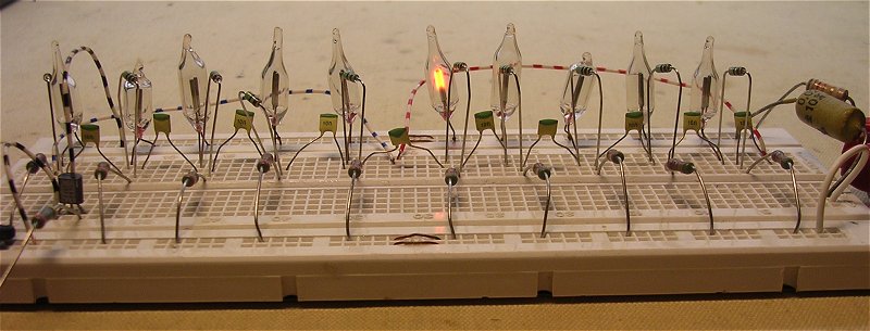
Figure 13. Ten stage Neon ring counter test circuit.
A quick measurement of ten tubes revealed that the striking voltage of the tubes varied between 93.7V and 101.4V with an average value of 97.5V, while the maintaining voltage varied between 66.4V and 72.0V with an average value of 68.6V, an average difference of 28.9V! According to the theory discussed in the previous section I should have first have to age the tubes and then have re-measured them again. This time however, I didn’t have the patience. The ideal cathode resistor for these tubes, assuming a current of 1 mA should have been 7k. In the absence of resistors with this value, I used 12k resistors instead (Fig. 13). Most Ring Counters have the count pulse capacitively coupled to the common anode node. I decided to use a high voltage transistor to pull-down the anode voltage to practically zero during the actual count pulse. This worked perfect, but it appeared absolutely necessary to include C0 to increase the rise time of the anode voltage. Without C0 the circuit would not function at all. For the count input pulses I used a TTL compatible signal with a 10% duty-cycle.
Although the component values were not ideal and the tubes had not been aged, the counter worked reliable for supply voltages between 185V and 250V up to a frequency of approximately 500kHz. For supply voltages below 185V the counter started to skip certain tubes in such a way that that tube would be skipped one cycle, but would strike the next one. For supply voltages higher than 250V, the counter started to count at twice the clock frequency
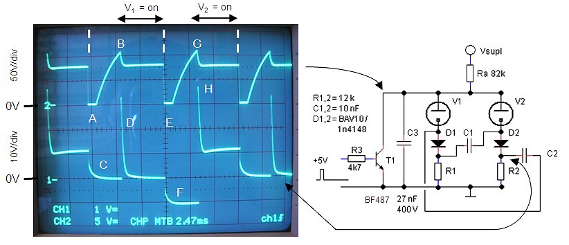
Figure 14. For the electrical characterization the length of the Ring Counter was reduced to two stages.
To enable electrical characterization of the waveforms of the signals inside the ring counter, the number of stages was reduced to two, a circuit also known as a toggle flip-flop. The upper trace in the scope image of Fig. 14 shows the common anode voltage, while the lower trace depicts the cathode voltage of neon tube V2. Both signals were measure using a 10:1 probe. At point A, transistor T1 is conducting so that the anode voltage is pulled down to practically zero, thereby extinguishing both tubes. When T1 is switched off, capacitor Co is charged through anode resistor Ra resulting in a logarithmic increase of the anode voltage (time constant τ = 82k * 27nF = 2.2ms). At point B the anode voltage has reached such a value that V1 strikes, immediately resulting in a reduction of the anode voltage to the maintaining voltage (ca. 75V). In the cycle prior to this cycle V2 was ignited. The current flowing through V2 resulted in a voltage drop over R2 which had charged C2 to approximately 10V. During the count pulse (point A), C2 is quickly discharged by R2 (point C) with a time constant τ = 12k * 10nF = 120µs. At point B capacitor Co is charged to ca. 105V. As soon as V1 strikes however, Co is discharged via R1 to Vm + I*12k. This sharp transient is amplified by the differentiating filter formed by C1 and R2, resulting in the sharp peak D.
During the time that V1 is on, the voltage drop over R1 charged C1 to approximately 1mA*12k = 12V. When next, during the next count pulse (point E), the voltage drop over R1 reduces to zero, the cathode of V2 will be biased to -12V: the cathode transfer bias (point F). When next the anode voltage rises again, V2 will strike (point G) ahead of V1 because of the negative transfer bias present on its cathode. Note that according to Fig.14 the striking voltage under dynamic conditions appears to be slightly higher than under static conditions (105+12=117V versus 97.5V). The sharp peak H of 30V is again explained by the rapid discharge of C0 from the striking voltage of 105V to the maintaining voltage of 75V.
Figure 15. Click here or on the picture to view a YouTube movie of the ring counter.

| to top of page | back to homepage |
In the section ”More on Neon Tubes”we already saw that there are two types of neon tubes: the barium coated tubes – which constitute perhaps more than 99.99% of all the neon tubes – and then the much rarer sputtered cathode tubes. The barium coated tubes have two advantages; firstly the bulb is not covered with metal - as would be the case for a sputtered cathode tube - so that the glow is clearly visible, and secondly in normal ambient lighting the breakdown delay is negligible due to photo-electric priming of the low work-function barium coated cathode.
Normal barium coated indicator tubes such as the NE2 of NT2, typically have a breakdown voltage in the order of 80-90V and a maintaining voltage of around 60V. The average difference between these two is therefore in the order of 20-30V. We have seen in the previous section that this is enough to make a logic circuit such as a ring counter, but it is certainly not large enough to make a robust design that can be produced
 on an industrial level and reliably operate over years despite aging of the tubes over time. Therefore special neon tubes were developed for switching applications. By optimizing the gas filling mixture and pressure and/or increasing the electrode spacing, tubes like the XC25 and XC26 were developed which gave breakdown voltages of 130-160V and 150-175V respectively, at the same maintaining voltage of ca. 60V. However, the problem of aging caused by diffusion processes in the barium layer remained.
The need for tubes with closer tolerances without aging phenomena, prompted Philips to develop a series of neon switching tubes with cathodes cleaned by metal sputtering. Cathode sputtering is a phenomenon which occurs in all gas discharge tubes. Ionized gas atoms (e.g. neon) are accelerated towards the cathode by the electric field. When they hit the cathode, they sometimes knock out a metal atom from the surface of the cathode. This atom then diffuses though the envelope of the tube and finally deposits on the anode or on the wall of the tube. During sputter cleaning the tube is heated to ca. 400C while at the same time the tube is operated at a very high current level. During this final production step the unavoidable oxide layer on the cathode is removed by sputtering from the cathode. At the same time the sputtered nickel or molybdenum atoms that diffuse though the tube will bind with any remaining oxygen atoms which are present in the gas. Finally, the deposited metal layer on the glass envelope will prevent the further out diffusion of contaminants from the glass. This elegant procedure was developed at Philips Research by Penning and Moubis in 1946. Their procedure for the first time allowed the fabrication of very stable voltage reference tubes like the 85A1 [3,p197]. In two papers in “Philips Research Reports” of 1946 they explain the principles of cathode sputtering [10] and metal gettering [11]. The papers give a very nice impression of the beautiful experiments which were carried out those days.
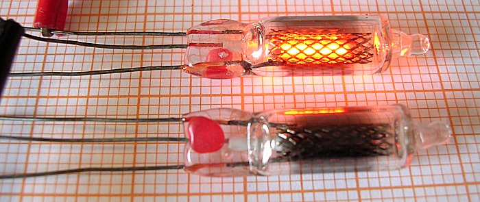
Figure 16. A ZA1002 switching tube (the scale is millimeter).
In the ZA100x series of neon tubes a special electrode structure is used to prevent complete covering of the inside of the tube with metal that would make the glow invisible. The tubes consist of a central molybdenum cathode rod, surrounded by a cylindrical anode in the form of a mesh. When the cathode is sputtered, material deposits on to the tube wall, to act as a getter, in a pattern corresponding to the holes in the mesh. As a result the wall of the tube is not completely covered with metal, leaving the glow clearly visible. An addition advantage of the concentrical arrangement is that slight deviations from concentricity do not substantially affect the field at the cathode, resulting in a decrease in tube-to-tube variations.
The ZA1000 and ZA1002 are switching “diodes”, the ZA1001 is a relaxation diodes suitable for timing circuits, while the ZA1003 and ZA1004 are indicator tubes suitable as read-out diodes for transistor circuits [3.p227]. The statistical breakdown of the tubes is reduced to less than 1 msec for a 10-20V overvoltage by the inclusion of a small quantity of tritium. The delay, however, is not reduced sufficiently for timing circuits where the tube acts as a relaxation oscillator at relatively low frequencies, and where it is essential for the tube to strike at the same voltage on each pulse. There is no problem at higher frequencies, since the tube does not have sufficient time to demonize completely between pulses, and there is sufficient residual charge to bridge the gap. To overcome the low-frequency problem the tube designed for timing circuits, the ZA1001, has a small quantity of heavy gas (Kr or Xe), which has a long deionization time, added to the main gas. So by combining a fast and slow deionization process in one discharge, the tube is able to oscillate over a comparatively wired frequency range.
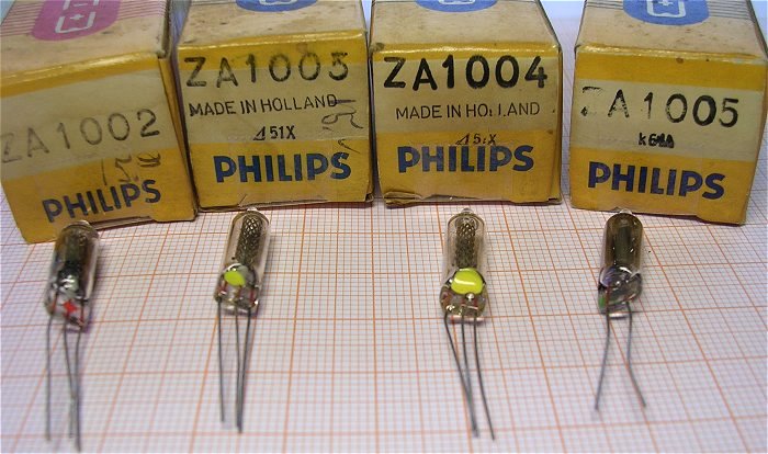
Figure 17. Some members of the ZA100x familie and their original boxes.
For applications as a read-out tube for transistor circuits the gas filling is chosen to give less spread in the breakdown voltage than the value of the signal supplied by the transistor. Examination of the breakdown voltage of gas mixtures shows that the breakdown characteristic of neon plus a small percentage of argon (e.g. 0.1%) has a flat characteristic at the Paschen minimum. This implies that the unavoidably small differences in the pressure and electrode spacing of individual tubes have hardly any influence on the breakdown potential. Using such a mixture, the spread of the striking voltage has been kept low enough for tube type ZA1003 to be controlled reliably by a 12V transistor, and type ZA1004 by a 6V transistor. The difference between breakdown and maintaining voltage for these tubes is low. For tubes types ZA1000 and ZA1002 used in differential circuits where a large difference between Vs and Vm is required, pure neon is used with a filling pressure higher than that corresponding to the minimum of the Paschen curve. With this gas filling, Vs-Vm is approximately 60V. For the seven ZA1002 tubes I have the (Vs,Vm) values are: (169.1,105.0), (171.0,105.2), (170.5,105.0), (170.0,104.8), (171.0,104.9), (170.0,104.9), (171.0,105.2). So a maximum variation in Vs of 2V and 0.5V in Vm! For these tubes the light output is rather higher than for the neon-argon filled tubes.

Figure 18. Datasheet for the ZA100x series taken from [9]
Click here or on the picture for a larger picture.
The ZA100x series switching tubes were presumably developed around 1961/1962, but were soon made obsolete by transistor switching circuits, and again a few years later by ICs. They are very rare. A search on Google only yielded a few hits. I had the luck to find a few ZA1002s in a long forgotten box of old stuff at the Philips Research lab. I had already lost all hope of ever finding some of the other tubes in the ZA100x series, when I happened to visit the shop of “Stuut and Bruin” [7] in (again) Den Haag (The Hague) [6]. Unfortunately “Stuut and Bruin” are really not in my way, so it must have been more than ten years ago since I visited them. It is an old shop that has been in business for more than 60 years. When I arrived at the shop, I was really perplexed to see a 6AL7 tuning indicator (magic eye) lying in the shop window! This tube has a top-view rectangular fluorescent screen, and is in Holland rather rare. It was the only 6AL7 the shop manager had in stock, because he had to fetch it from the shop window, which according to him hadn’t been opened in twenty years (I am sure he exaggerated a bit). I was so enthusiastic about the tube that he gave it to me for free! I decided that this must be my lucky day, so I asked the manager if he had ever heard of the ZA100x neon tubes series. After looking at me for a few moments as if had been struck by lightning, he beckoned me to come behind the counter to a dark corner in his shop where he had a wall full of NOS tubes, most of them from Philips, and all still in their original cardboard boxes, most of them a bit affected by mould in this presumably damp corner. To my astonishment he produced almost the complete ZA100x series from this marvelous collection (Fig. 17). In the picture the boxes still carry the original prices (in guilders) of fl 15.00. Today this is about 6.50 euro, but 30 years ago it corresponded to 25 euro [8].
| to top of page | back to homepage |
Being the proud owner of seven ZA1002 tubes, I obviously wanted to make and test a ring counter using these tubes. I used the circuit of Fig. 13 with some modifications to the component values. Rather than using the nominal anode current and then arriving at non standard resistor values, I used a standard value of 47k for the cathode resistor and calculated the current from I = (Vs–Vm)/2*Rcat = (170-105)/2*47k = 690 µA. With an anode resistor of 100k, the nominal supply voltage then amounts to Vsupl = I*(Ra+Rcat)+Vm = 690µA*(100k+47k)+105 = 206V. Since it was already very easy to obtain a reliable counter using the cheap barium cathode neon tubes, I expected the counter with the ZA1002 to function very robust over a wide supply range. I was however completely stunned and mystified to find that it was absolutely impossible to obtain anything near reliable operation with these tubes!
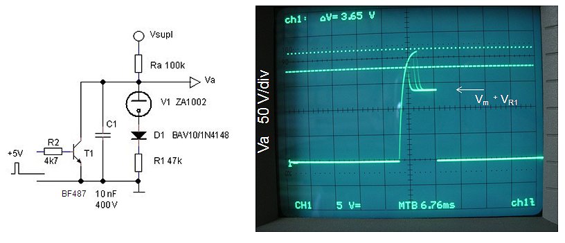
Figure 19. Stripped down ZA1002 ring counter and the waveform of the anode voltage.
I tried different combinations for cathode resistors and supply voltages, but the working of the counter remained almost completely erratic, almost random. After messing around with the circuit for some time, the reason for the strange behavior of the counter became clear when I stripped down the counter to just one tube. Figure 19 shows the stripped down circuit and the waveform of the anode voltage. From the scope trace it appeared that the tube strikes randomly at voltages between 170 (as it should be) up to voltages of 220V. In the photograph of Fig. 19 four traces were recorded during one camera exposure. Observe that after the tube has ignited, the voltage drops to a constant value determined by the maintaining voltage and the voltage drop over the cathode resistor.
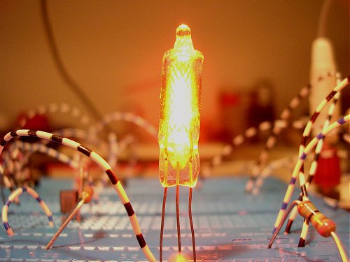
Figure 20. a ZA1002 during sputter cleaning of the cathode. The cathode seems brighter on the photograph than it was in reality.
The first explanation that I could think of for this strange behavior was that one way or the other, over the years, the cathode had been contaminated again. In Weston’s book on cold cathode tubes, it is explained that cold cathode tubes are typically sputtered at approximately ten times the nominal anode current, until the cathode is red hot [3]. Figure 20 shows a ZA1002 at a cathode current of 10mA. Within a few minutes the tube is so hot that I literally burned my fingers touching it. The procedure didn’t have any effect at all.
Finally, it dawned on me that the problem could also be related to the priming of the tube. Recall, that in order to reduce the turn-on time of the tube to less than 1ms, a small amount of tritium was added to the neon gas. The effect of the radio-active tritium is that it ionizes some of the gas molecules, so that always sufficient ions are present to ensure fast striking of the plasma. A quick search on the internet learned that the half-life of tritium is about 12.3 years! This means that every 12.3 years, half of the tritium decays into helium-3. In other words sixty years after their production (1/2)**(60/12.5) = 1/64 only one 64th of the tritium is left. In other words the tube is hardly primed resulting in a variable striking of the tube. The strange thing is that although almost every tube regardless its age will remain more or less function as long as the filament is still intact and has some emission and there is no leakage, these tubes inherently have a limited shelf life. Obviously the people at Philips could not have imagined that some fool would be playing around with these tubes sixty years after their production, otherwise they surely would have added a “best before …” warning!
| to top of page | back to homepage |
There is this constant rumor in news-groups on the internet that it is possible to build a nixie counter just using a hand full of diodes and resistors. Undoubtedly, these rumors find their origin in the notion that a nixie tube is nothing more than ten separate neon tubes combined into one envelope with a common anode. Looking at the basic neon ring-counter circuit shown in Fig. 13, it is indeed tempting to think that it is possible to replace the ten separate neon tubes by one nixie tube (Fig. 21).
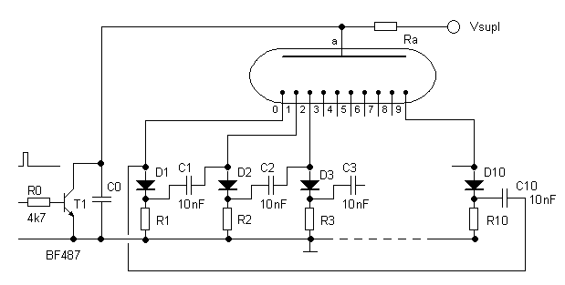
Figure 21. Replacing ten neon tubes by one nixie tube does not work.
I have to admit that originally I could see no reason why this should not work! However, a quick try did not result in a functional counter. One explanation is that the difference between striking and maintaining voltages of nixie tubes appeared to be very small. For several nixie tubes the measured (Vs,Vm) values were: ZM 1020=(133,123), IN12=(132,125), XN12=(128,124), ZM1080=(131,125), ZM1040=(127,125), CD83P=(122,119). Furthermore, it appeared that once one of the digits is ignited, the other digits become so fully primered that their striking voltage is reduced to the maintaining voltage of the digit already on. In fact, it is difficult to speak of striking since the new digits switches on very gradually when the cathode potential approaches the maintaining voltage. So, at first sight, the on-voltages of all digits become more or less equal. This suggested the circuit of Fig. 22A.
Figure 22. Another non-functional ring counter circuit.
In the circuit of Fig. 22A it is assumed that once the nixie tube has ignited, the voltage drop for each of the digits is equal, and as such would only represent a constant voltage drop so that the nixie tube could be incorporated in series with a standard neon ring counter. Alas, this circuit also did not function. In a three stage test version all three digit ignited at the same time. The simple test circuit of Fig. 22B shows the reason. If my assumptions were correct, and indeed the ignited nixie tube would represent a constant voltage drop for each of the digits, it would be impossible to ignite V2 by pressing S1. This was however not the case. The ignited nixie tube obviously represents a very complex load, where a not connected digit assumes a potential somewhere in between the anode potential and the potential of the cathode already ignited.
p.s.: Based on the experiences with the Shockley diode ring counter (Fig. 30) I think I will have one last go at making this circuit work by tying the cathodes of the nixie to a constant potential via a resistor. Fact remains that the on-current for most nixies is a bit too high for most neon indicator tubes.
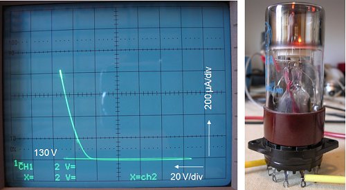
Figure 23. A GR10A Register tube from ETL (Ericsson Telephone Limited) England.
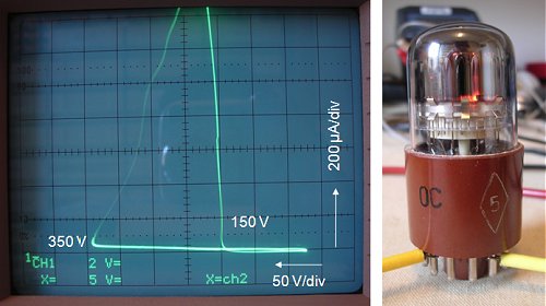
Figure 24. A Russian A-101 Register tube
| to top of page | back to homepage |
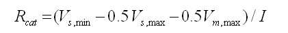
During the experiments described in the next section I felt the need for a curve-tracer. A curve-tracer is a piece of test equipment that displays the current-voltage relationship of a component on the screen of a CRT. In this way you can, for example, find in one glance the striking and maintaining voltages of a neon tube. We have a beautiful Tektronix 370A curve-tracer at work, but it being Christmas holidays at the writing of these pages, that was of little help to me. However, with a few components that almost everybody has lying around, it appears possible to built a really very useful poorman’s curve-tracer in less than ten minutes!
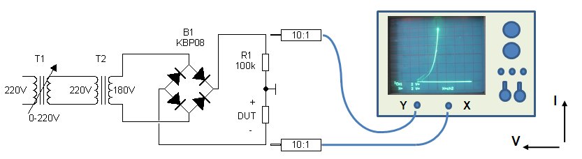
Figure 25. Circuit diagram of the poorman’s curve-tracer.
Figure 25 depicts the circuit diagram of the poorman’s curve-tracer. Variac (T1) and a fixed transformer are used to obtain a variable AC voltage source of 0–250 V (250 = sgrt(2)*180). The AC voltage is double-sided rectified by bridge B1, resulting in a halve-sinewave voltage with an adjustable amplitude of 0–250 V. Series resistor R1 measures the current through the Device Under Test (DUT). My scope allows for the timebase to be switched off in such a way that the channel 2 input becomes connected to the x-axis deflection plates. By connecting the ground of the scope to the node connecting the DUT to R1, and the y-plates (channel 1) to R1 and the x-plates (channel 2) to the DUT, it becomes possible to measure the I-V curve of the DUT. The only drawback of this circuit is that the x-axis is displayed inverted meaning that positive voltages are displayed in the negative x-axis direction. A small inconvenience that you quickly get used to.
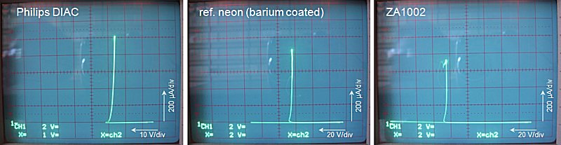
Figure 26. Three examples of I-V curves measured with the poorman’s curve-tracer. The DIAC was a BR100/03 from Philips.
 square from the lower-right corner of the plot. Starting at the origin the voltage across the DUT increases with no current flowing. At about 33V the DIAC is triggered resulting in a current flowing, while the voltage drops to ca. 27V. The very small difference between the
“striking” and “maintaining” voltages of this DIAC, shows that unfortunately it is pretty useless as an active element in a ring-counter. The neon tube has a striking voltage of 115V with a maintaining voltage of 65V. The ZA1002 tube has a striking voltage of 175V with a maintaining voltage of 105V.
square from the lower-right corner of the plot. Starting at the origin the voltage across the DUT increases with no current flowing. At about 33V the DIAC is triggered resulting in a current flowing, while the voltage drops to ca. 27V. The very small difference between the
“striking” and “maintaining” voltages of this DIAC, shows that unfortunately it is pretty useless as an active element in a ring-counter. The neon tube has a striking voltage of 115V with a maintaining voltage of 65V. The ZA1002 tube has a striking voltage of 175V with a maintaining voltage of 105V.
Note, that most variacs are “autotransformers”, meaning that they do not have a separated primary and secondary windings, but only one winding with a variable tap. In such a transformer the secondary side is not isolated from the mains, and can be deathly on touch even for small output voltages. Despite the fact that the variac of Fig. 25 shows two windings, also my variac is an autotransformer (I didn’t have the correct symbol). That is why T2 was added to isolate the circuit from the mains. If you are not familiar or comfortable with circuits that are connected directly to the mains please read my introduction to this topic on my Tube-in-a-Tube clock page. If you are not in the possession of a variac, you can just as well use a single transformer with a fixed output voltage that is high enough. The high value of R1 will limit the current through the DUT, and therefore the dissipation. To be on the safe side, make R1 a 1W type.
For my own convenience, here is the procedure to set-up the scope:
| to top of page | back to homepage |
Already four years before the war, in 1936, the visionary research director of Bell Labs - Mervin Kelly - hired the young and brilliant physicist William Shockley to investigate the possibility of a rugged solid-state device that could replace the unreliable switches and tubes which were used in telephone systems those days [12]. Recent advances in quantum mechanics and solid-state physics had suggested several device concepts to Shockley, but all of these devices failed to function as he had hoped. With hindsight, this was mainly due to the fact that in the pre-war period there were no good and pure semiconductor materials available, besides this there was still little understanding of the physics of semiconductor surfaces.
 World War II interrupted Shockley’s efforts when he took leave from Bell Labs to become a research director at Columbia University’s Anti-Submarine Warfare Operations Group. However, the enormous research efforts during the war on radar resulted in tremendous advances in the understanding, fabrication and purification of both germanium and silicon, since these materials were essential for the fabrication of reliable and sensitive point-contact radar detectors.
Directly after the war, Shockley returned to Bell Labs to head a solid-state physics group whose mission it was to come up with a solid-state alternative for vacuum tubes. Again, Shockley had an idea for a semiconductor amplifier, and again it didn’t work. Nobody could understand why, and discouraged he turned to other projects, leaving the conundrum to Bardeen and Brattain. In the course of their research, they discovered that the reason why the devices of Shockley failed was due to the presence of interface states at the surface of the semiconductor. During their investigations, they subsequently more or less stumbled upon the point-contact transistor! When the patents were drawn, Bardeen and Brattain consequently were the sole inventors.
Shockley was disgusted by the fact that despite that he had been searching for a solid-state amplifier for such a long time, he was not one of the inventors of the point-contact transistor. He locked himself up for nearly a month, trying to design an even better device. In a review paper of 1976, Shockley himself recapitulated the process of thought that took place during that time in a section titled “The Will to Think.” [17] Near the end of that month, Shockley had figured out the important details of a device of his own design, the junction transistor. The junction transistor did not rely on quirky point-contacts, but only required a small stripe of silicon or germanium with differently doped regions. Although it still would take years before technology had advanced to such a level that the junction transistor could actually be made, Shockley was fully confident of the superiority of his device, a fact he never failed to tell Bardeen and Brattain. Obviously, the relationship between the three men deteriorated and in 1951 Bardeen and Brattain left to pursue other interest. In 1956 Bardeen, Brattain and Shockley were once again reunited when they received the Nobel Prize for their work.
His reputation allowed Shockley to raise the funds to setup his own business. In 1956 Shockley hired a building in an obscure valley south of San Francisco, then filled with apricot orchards, founding the first company in what is now called Silicon Valley: “Shockley Semiconductor Laboratory.” His Initial plan was to develop silicon transistors, in a time when almost all transistors were made out of germanium [13,14]. However, after some time his interest in transistors faded, and Shockley became obsessed by the “four layer diode”, a device he had invented while still working at Bell Labs. Instead of focusing on transistors to have at least one cash generating product, an enormous amount of development effort was spent on the four layer diode which proved very difficult to fabricate.
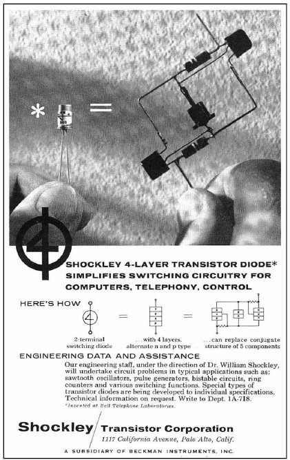
 The four layer diode, also known as Shockley diode was a switching device that could replace at least two transistors and two resistors [15]. As such it really was the first integrated circuit. It is a two terminal device that is non-conducing until the voltage over the diode is increased beyond a certain value. At that moment, the diode abruptly starts to conduct, and it remains conducting until the voltage over the device is decreased below the turn-off voltage. As such the device represents a single bit memory, while it also proved useful in ring counters and oscillators. The device has its own circuit symbol resembling the digit 4. It was however for that time far too complicated [16]. It required accurately double sided polished silicon wafers with junctions diffused from both sides. The final mesa device additionally was extremely sensitive for moisture. Shockley hoped that it would eventually replace the millions of mechanical switching points in telephone systems. However, the spead in device parameters proved to be too large to be acceptable for AT&T. In the end it turned out that Shockley was a far better a scientist than a business man. His management style was domineering and increasingly paranoid, which in the end resulted in eight key employees (the traitorous eight) leaving the company to start their own company: “Fairchild Semiconductor.” A few years later, Fairchild was one of the first companies to produce integrated circuits, making Shockley’s four layer diodes obsolete. In April 1960 Clevite Transistor Company purchased Shockley Transistor Compagny.
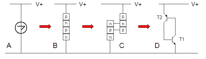
Figure 27. Symbol A) and four layer structure B) of the Shockley diode. The four layer structure can be thought of as an npn and pnp structure C) and D).
Figure 27A shows the circuit symbol that was used for the Shockley diode. If the symbol is rotated by 180 degrees as in the advert above, we see that the symbol resembles the number 4. The best way the explain how the four layer diode (Fig. 27B) works, is to think of it as an npn and pnp structure connected as in Fig. 27C, or an npn and pnp transitors with the base of each transistor connected to the collector of the other (Fig. 27D).
To explain how the device works we assume for a moment that we have an external connection to the base of T1. Assume that T1 has a DC current gain hFE1 (Fig. 28A). The application of a small external base current Ib will result in an amplified collector current Ib*hFE1. If we next connect the collector of T1 to the base of a pnp transistor T2, then the collector current of T1 will be the base current of T2 (Fig. 28B). This base current is amplified by a factor hFE2 by T2, resulting in a collector current of T2 of hFE1*hFE2*Ib. When finally the collector of T2 is connected again to the base of T1, the collector current of T2 will drive T1 etc. Through this positive feedback a current will continue to flow through T1 and T2 - even after removal of the external base current - provided that the condition hFE1*hFE2>1 is satisfied.
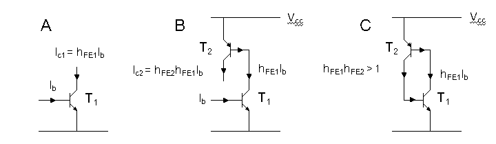
Figure 28. Working of the Shockley diode explained using the two transistor equivalent circuit.
The device with external base connection is of course also known as a thyristor! By removing the external base contact we obtain the Shockley diode. This device remains in the off-state until the supply voltage approaches the collector-emitter breakdown of one of the transistors. Approaching the breakdown a small avalanche current will start the flow. This current is immediately amplified, and because of the positive feedback loop, the circuit will immediately latch, with the voltage across the two terminals dropping to practically zero. The circuit can only be reset by interrupting the current.
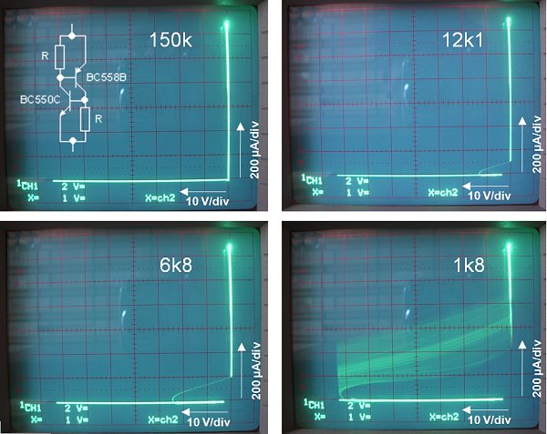
Figure 29. Effect of different values for the emitter-base shunt resistor.
Shockley diodes are no longer produced, but fortunately we can emulate their functionality with two transistors. With normal discrete transistors hFE1*hfE2>1 is easily satisfied, in fact the gain is usually so high that it is almost impossible to prevent unwanted latching of the circuit. The circuit can be tamed by shunting the emitter-base junctions of the transistors with resistors. As we will see in the next section, this will reduce the gain of the transistors for small currents. In Fig. 29 we see for different values the effect of this resistor. For R=150k the circuit behaves as an almost perfect switch. The curve starts in the origin (lower-right corner) with V=0. From the origin we move to the left over the horizontal line as the voltage across the circuit increases while the current still remains zero. When the voltage reaches ca. 73V, the circuit latches, and the curve jumps from the lower-left point to the upper-right point, representing a current of 1.3mA with negligible voltage drop. With decreasing supply voltage the current decreases proportionally, until we arrive back at the origin. For R=12k the curve is nearly identical, only near the very last part of the curve, when current drops below ca. 100uA, the loop-gain drops below unity so that the circuit drops out of latch. The lower the resistance the higher the current at which the circuit de-latches.
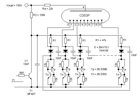
Figure 30. Ring counter circuit with emulated Shockley diodes that directly drives a nixie tube.
Our emulated Shockley diode is of course an ideal element to replace a neon tube in a ring counter. The enormous difference between the “striking” voltage and the on-state voltage drop allows for a very robust design. Figure 30 depicts a three stage ring counter circuit which directly drives a nixie tube. Apart from the nixie tube, the circuit precisely follows the classical ring counter circuit with the neon tube replaced by the emulated Shockley diode. A 12k resistor was used in for the emitter-base shunt in the “Shockley diode”, since this value gave a good compromise between sensitivity and robustness (Fig. 29). The values of R1, R2 and Ra determine the static biasing conditions.
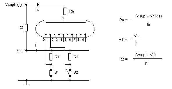
Figure 31. Determination of R1, R2 and Ra

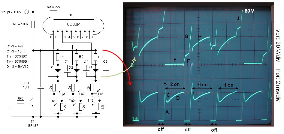
Figure 32. Dynamic behavior of Ring counter with emulated Shockley diodes.
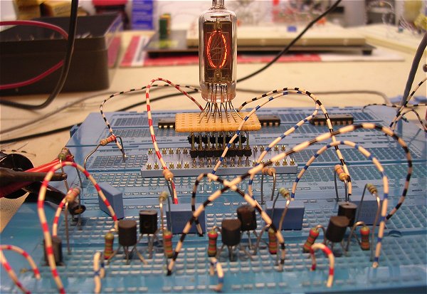
Figure 33. Click here or on the picture to view a YouTube movie of the ring counter with emulated Shockley diodes.
| to top of page | back to homepage |
Although the ring counters with the emulated Shockley diodes work very satisfactory, I was left with the question if it would be possible to make a circuit that would exhibit a suitable hysteresis using only one transistor instead of two. After some thinking, I remembered a phenomenon that I often observed during the measurement of high frequency bipolar transistors. Between 1988 and 2000 I spent most of my time at Philips Research with designing and actually fabricating high performance, high frequency bipolar transistors, mainly for mobile communication. One of the standard measurements we used to perform on a freshly made transistor was the measurement of a set of Ic-Vce curves on a curve-traces. This quick measurement gives a good first impression of some of the main DC transistor parameters such as: hFE, Veaf, BVceo, linearity, collector resistance, etc.
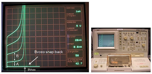
Figure 34. Set of Ic-Vce curves of a BF771 measured on a 370A Tektronix
Crve-traces.
The transistor exhibits a drop in hFE for currents smaller than 1mA.
Figure 34 shows a set of Ic-Vce curves of a BF771 high frequency transistor. During the measurement, the collector-emitter voltage (horizontal axis) is swept from zero to an adjustable maximum value, while the collector current is being measured (vertical axis). The base current is incremented every sweep by a constant value (20 µA in this case), starting with Ib=0 for the first sweep.
Since the increment in Ib is constant for every sweep, the DC current gain (or hFE, or beta) per vertical division is known (50 per div. in this case). By counting the number of divisions on the vertical axis between two successive lines, the hFE can be determined at that bias point. For a perfect transistor the hFE should be constant from current levels in the pA range, up into the regime where series resistances and
 high injection effects start to play a role (order 10-100mA for normal discrete transistors). However, for this transistor we observe that at Ic=5mA the hFE=80, while it drops well below 50 for Ic<1mA. Indeed, if we
would have measured the hFE at even lower current levels, we would have seen that the hFE would drop to zero. This effect is for this type of transistors caused by leakage currents at the edge of the emitter, which in turn are caused by imperfections in the production process. Since high frequency transistors use a multiple multi-finger emitter structure with narrow emitters rather than one large rectangular or round emitter, high frequency transistors have relatively a lot of edge and hence a lot of leakage current which will kill the hFE in the low current regime.
high injection effects start to play a role (order 10-100mA for normal discrete transistors). However, for this transistor we observe that at Ic=5mA the hFE=80, while it drops well below 50 for Ic<1mA. Indeed, if we
would have measured the hFE at even lower current levels, we would have seen that the hFE would drop to zero. This effect is for this type of transistors caused by leakage currents at the edge of the emitter, which in turn are caused by imperfections in the production process. Since high frequency transistors use a multiple multi-finger emitter structure with narrow emitters rather than one large rectangular or round emitter, high frequency transistors have relatively a lot of edge and hence a lot of leakage current which will kill the hFE in the low current regime.
Another important parameter that easily can be determined is the BVceo. This is the collector-emitter breakdown with open base (Ib=0). In Fig. 34 this point is indicated by the arrow with the text “BVceo snap-back”. This is exactly the phenomenon I was referring to! After the transistor breaks-down at approximately 18V, the break-down voltage drops back to 15V for increasing collector current. This negative resistance or hysteresis behavior resembles the behavior of neon tubes, and in principle could be used to construct a ring counter. The difference between “striking” voltage and “maintaining” voltage is however way too small to achieve reliable operation.
To understand the phenomenon of BVceo snapback, it is important to understand the difference between the BVcbo (the breakdown of the collector-base diode with emitter not connected) and the BVceo (the breakdown between collector and emitter with open base). In one of my other pages, I have gone to great length to explain the relation between these two breakdowns. Here it is sufficient to know that the BVceo relates to the BVcbo according to:
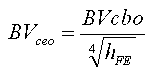
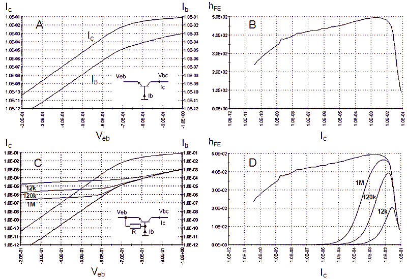
Figure 35. Gummel plot and hFE-Ic curve for a BC550C (A and B),
and for a BC550C with different emitter-base shunt resistors (C and D).
As mentioned before, the effect is usually much too small to use it for the construction of a ring counter. Fortunately, it is possible to induce the snap-back effect in every healthy linear transistor by means of a simple resistor. Figure 35A depicts a so called Gummel plot and an hFE-Ic curve (Fig. 35B) of a common, low-voltage, general purpose BC550C. A Gummel plot is a measurement whereby the collector and base currents are measured as a function of emitter-base voltage for constant collector-base voltage. This measurement, whereby the transistor is used in common-base configuration, gives a lot of information on the emitter-base construction of the transistor and is primarily used by technologist to evaluate the emitter-base complex of a transistor (the Ic-Vce curves yield more information on the collector construction). The vertical distance between the collector and base current exactly corresponds to the hFE when both currents are plotted on a logarithmic scale. From the figures it can be seen that a BC550C has a maximum hFE of ca. 500, while the hFE is still well in excess of 100 for Ic=1pA. In other words a perfect highly linear transistor! The linearity can be completely ruined by shunting the emitter base with a resistor (Fig. 35 C and D). The resistor emulates an emitter-base leakage current which will – depending on the resistance value – completely dominate the current gain at low current values (Fig. 35D).
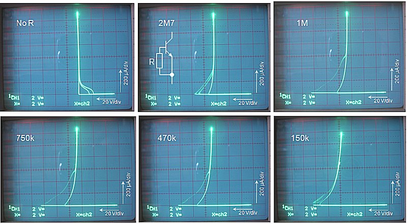
Figure 36. Effect of the emitter-base shunt resistor on the artificially induced snap-back.
From the preceding it will be clear that a normal BC550C does not exhibit a snap-back behavior (Fig. 37 No R). However, by adding a high-value emitter-base shunt resistor, a snap-back can be induced. The different graphs in Fig. 36 show the induced snap-back effect for different values of the shunt resistor. For R=1M we have a nice sharp snap-back whereby the transistor breaks down at the BVcbo of 125V, and then quickly falls back to a BVceo of 65V. A difference of 60V, more than enough to make a very reliable ring counter!
The BC550C is a typical European transistor. It is very cheap, Farnell charges less than six euro cents! Instead of the BC550C also other transistors can be used. The most important selection criteria are in the first place a BVcbo that is not too high (say 80-130V). Secondly, the transistor should have an hFE as high as possible to obtain a large difference between the BVcbo and BVceo. For the BCxxxC transistors the last letter indicates the hFE binning group. The C group has the highest hFE (400-600). Finally, the transistor should have a reasonable linearity so as not to interfere with our trick.
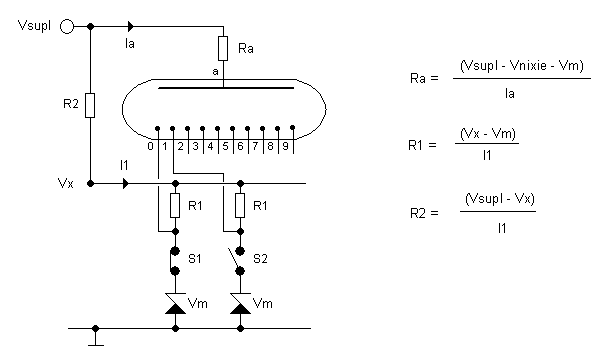
Figure 37. Determination of R1, R2, and Ra
The circuit diagram of the ring counter with “snap-back transistors” closely resembles the “Shockley diode” ring counter (Fig. 38). Before discussing the circuit and its signal waveforms in detail, we will first calculate the resistance values which will determine the bias conditions.
Figure 37 shows the ring counter circuit stripped of all components irrelevant for the determination of the biasing resistors. The snap-back transistors have been replaced by switches S1 and S2, and by two zener diodes with a value Vm. Vm in the following represents the BVceo (65V) and Vs represents BVcbo (125V). Similar to the procedure followed in the previous section we first need to establish some essential parameters:
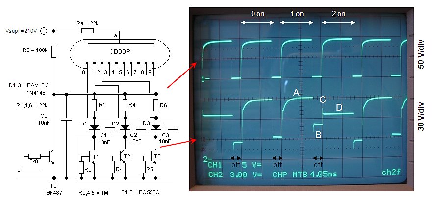
Figure 38. Three stage ring counter test circuit using the “snap-back” transistors.
Figure 38 depicts the circuit diagram of a three stage test ring counter using the “snap-back” transistors (left) and its associated signal waveforms (right). At first glance the signals are all very well behaved without too much spikes and transients. The upper signal trace shows the signal at point Vx (Fig. 37). At every counting pulse transistor T0 is driven into saturation, pulling Vx to ground. In between counting pulses Vx returns to 95V as it should. The arrows above the upper trace indicate which nixie digit is switched on during three consecutive counting pulses. At point “A” T2 is on so that C2 will be charged to 30V. During the next counting pulse (point “B”), C2 remains charged giving T3 a “pre-bias” so that it will “strike” first when Vx returns to 95V (point “C”). After T3 ”strikes”, the voltage drops back to the “maintaining” voltage of 65V (point “D”).
Figure 39. Click here or on the picture to view a YouTube movie of the ring counter.
If you watch the YouTube demo-movie of the “snap-back” ring counter carefully, you will see that the circuit has one flaw: during the actual counting pulse, when T0 is conducting, all digits ignite. Obviously, this is caused by the fact that when Vx is pulled to ground to bring T1 … T3 out of avalanche, also the cathodes of the nixie tube are grounded. Personally, I think it is quite a charming artifact, but I you do not like it, it can easily be remedied by adding an additional transistor in parallel to T0 but with the collector connected to the anode of the nixie tube. Note that in this case this has to be a transistor with a BVcbo of at least 185V!
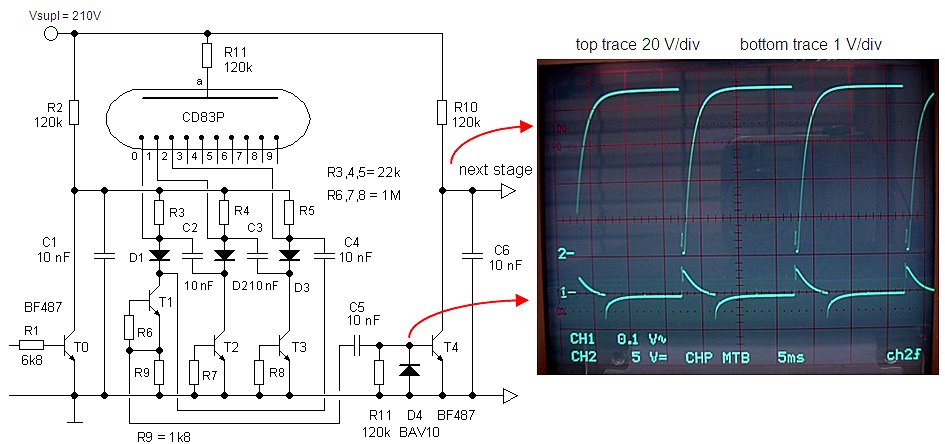
Figure 40. Three stage “snap-back” transistor ring counter circuit with carry circuit for cascading counting stages.
It is very simple to add a carry circuit to the ring counter for the cascading of counting stages (Fig. 40). When a roll-over from digit 2 to digit 0 occurs (a carry in this three stage example) a current will start to flow through T1. This will result in a voltage drop of about 2V over resistor R9. This voltage drop is so small that it will not effect the operation of the ring counter. After differentiation of this pulse by C5 and R11, this pulse will briefly drive T4 - which is part of the next counting section - into saturation, thereby advancing the next counting section.
Personally I find the “snap-back” ring counter a very elegant nixie counter/driver solution. It does not require obsolete power-hungry TTL circuits, nor does it require special high-voltage transistors. The counting range can easily be modified just by reducing (or expanding) the number of counting stages. I did not attempt to build a clock based on these circuits myself, but I am sure I will one of these days.
| to top of page | back to homepage |
I have made it a kind of a hobby to find un-orthodox ways to drive nixie tubes. With my Tube-in-Tube clock I have tried to demonstrate that in some cases low-voltage transistors can be used to drive a nixie tube, and on this page also a few remarkable nixie counter/driver circuits have been discussed. The driver circuit discussed in this section can no doubt also be regarded as remarkable. The idea came upon me when I was working on a circuit with a ZM1050 tube. It occurred to me that the same basic principle that underlies the ZM1050 tube, can also be used to safely and reliable drive a nixie from a HEF4xxx or CD4xxx gate, provided that they are operated from a 15V supply voltage. Although the circuit is of little practical value, it serves as a nice introduction to the sections dealing with the ZM1050. In the remainder of this page when I write ZM1050 it also means ZM550, and when I write HEF4xxx you can also substitute CD4xxx.
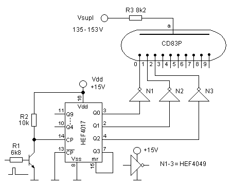
Figure 41. The simplest, but not the most elegant way of interfacing a HEF IC to a nixie tube.
The most straightforward way of tying a nixie tube to a HEF4xxx gate is shown in Fig. 41. The working of the circuit is based on the fact that the strike and maintaining voltages of most nixie tubes almost coincide.
It appears that the 15V output voltage swing of a HEF gate is large enough to switch a digit on and off. When, for instance, the output of inverter N1 is low while the outputs of the other gates are high, only the zero digit will ignite. Many people will be hesitant to tie the output of an HEF gate directly to a device that is connected to a high voltage supply. In reality there is no harm in this. The main reason is that the current is limited to at most 2 mA. In case the output of the gate is low, the NMOS transistor at the output of the gate will simple sink this current to ground. When the output is high, the output protection diode will sink the current to the positive supply voltage rail of the HEF IC. Even if the IC wouldn’t have an output protection diode, the drain-nwell diode of the output PMOS would become forward biased, again sinking the current to the Vdd rail.
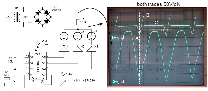
Figure 42. Driving neon lamps driven by a HEF4xxx gate.
If we were to try to do this with the neon tubes that were used in the previous sections, it wouldn’t work. The neon tubes have a hysteresis of about 40V (Fig. 26) which would make it impossible to switch the tubes on and off. There is however a very clever way to make it work. The trick is to use a half-wave or full wave rectified AC voltage as power supply. Figure 42 illustrates this idea, and the working is actually very simple.
We start at the moment the mains voltage crosses zero volts (point “A”). The neon tubes are now obviously off. Next, the supply voltage starts to increase. Note that since the neon lamps are not ignited, the current is zero and hence there is no voltage drop across R3, so that the voltage at the common anode node (upper trace) equals the supply voltage (lower trace). Now assume for the moment that the output of inverter N1 is low, while the outputs of the other inverters are high. In that case, when the supply voltage increases, neon tube V1 will obviously strike first (point “B”). The voltage across V1 now immediately drops to the maintaining potential of 65V so that none of the other neon tubes can strike, even if the supply voltage increases even further. V1 thus remains ignited during this whole half phase of the mains frequency (“C”), even if one of the other inverters becomes low. At the next zero-crossing V1 is reset (point “D”), and the whole cycle starts all over again.
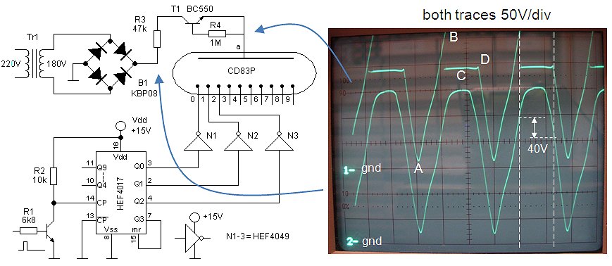
Figure 43. Nixie tube driven by a HEF4xxx gate and a pulsating HV supply.
Figure 44. Click here or on the picture to view a YouTube movie of the Nixie being driven by a HEF4049 with a pulsating DC voltage.
| to top of page | back to homepage |
In this section we will discuss the technical aspects of the Z550M, in the next sections we will have a look at the people who invented it and turned it into a product. The Z550M is best introduced by quoting the introductory paragraph of section 10.3 from “The Z550M Indicator Tube” by J.B. Dance [2]:
| The Mullard/Philips Z550M is a unique tube which has been developed to satisfy the need for a decade indicator tube which can operate directly from the low voltage electrical readout provided by transistor scalers (counters). It requires an input signal of about 5V at a current of about 50 µA. The form of the display is different from that of other indicator tubes. Ten figures are cut in the anode in the shape of the digits to be indicated; they are arranged in a circle, each digit being 3 mm in height. A gas discharge takes place behind one of the digits so that red light from the discharge shines through the cut away portion of the anode in the form of the digit to be indicated. The display can be quite bright, since the control circuit does not supply the power to the main discharge. |
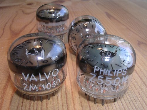
Figure 45. The ZM1050/Z550M with labels Philips and VALVO.
In fact all ZM1050s were made at the main tube production side of Philips
at the “Emmasingel” in Eindhoven, the Netherlands (see Epiloque).
The working of the ZM1050 resembles the working of the circuit discussed on my ring counter page. The basic idea is that ten glow-discharge tubes, with very matching characteristics, are integrated into one envelope. The tube is fed with a half-sinewave voltage in such a way that the small additional voltage from a transistor preferentially ignites one of the ten glow-discharges. Next, the common anode voltage now drops so that none of the other glow-discharges strike. A special provision has been made so that the striking of each discharge is initiated by a separate “starter anode” which is driven by the transistor and requires only a very small current. This auxiliary discharge is then transferred to the main discharge at a much higher current level. A more exact and complete explanation of the working can be found in an article by one of the inventors, Theo Botden, in “Electronic Applications” [3]:
Figure 6 shows the arrangement of the electrodes of the Type Z550M (ZM1050) indicator tube. The ten approximately trapezoidal plates k act as emissive cathodes. They are mounted on a ring-shaped conducting support r, the shaded sections of which are coated with a material having a high work function compared with the cathodes k to reduce their electronic emission. A short distance above and below the cathodes annular anodes a are mounted. Ten wire electrodes st, the starters, protrude through holes in the lower anode ring and in each of the cathode sections. In the upper anode ring the figures from 0 to 9 are cut out, so that when a glow discharge is initiated by means of one of the starters, the figure facing the corresponding cathode clearly stands out. Figure 7 shows an exploded view of the electrode system. The emissive cathode sections have been “sputtered” during the manufacturing process to obtain clean cathode surface, whilst the sputtered material settled on the glass envelope prevents contamination of the gas, and thus ensures stable operation. The tube is filled with neon to which a small percentage of argon is added.
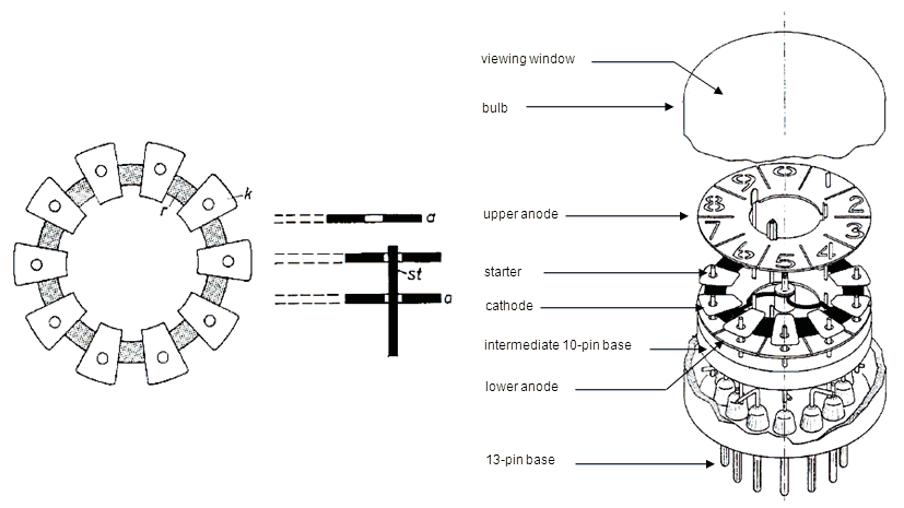
The tube is fed with an unsmoothed rectified voltage (see Fig. 8), so that with half-wave rectification, the supply voltage rises to a maximum and drops to zero again once in every mains cycle. When the supply voltage reaches a certain value, a glow discharge is initiated which extinguishes again as soon as this voltage drops below the maintaining value. The glow discharge is thus obviously ignited and extinguished twice per cycle when full-wave rectification is employed. As can be seen from Fig. 8, the starters are at anode potential as long as there is no discharge. However, as the distance between each cathode and its associated starter is much smaller than that between the cathode and the anodes, a discharge between cathode and starter will be initiated before the supply voltage has risen to the value at which a discharge between the cathode and anode is established. When, therefore, the supply voltage progressively rises from zero, the first effect will be the initiation of an auxiliary discharge between the cathodes and its starter. The operation of the Type Z550M (ZM1050) indicator tube is based on the fact that an auxiliary discharge between one of the cathodes and its starters reduces the required anode ignition voltage Vaign between this cathode and the anode to such an extent that the main discharge is also established at this cathode. It thus suffices to make a provision for an auxiliary discharge to be established at the desired cathode to ensure that the main discharge occurs at the corresponding figure. This main discharge causes the anode potential to drop suddenly to the maintaining voltage Vm which is below the lowest ignition voltage at any other cathode, so that no discharge can be initiated elsewhere. In other words, “first come, first served” applies; at any rate as far as that particular cycle of the supply voltage is concerned.
The dependence of Vaign on the starter current Ist is plotted in Fig. 9 for one of the starter-cathode positions. It is seen that when the starter is disconnected (Ist=0) the voltage required for initiating the main discharge is approximately 135V, but at a starter current of, say, Ist=10µA, this voltage is reduced to approximately 105V, which is mainly due to positive and negative charge carriers diffusing from the auxiliary discharge to the space between this cathode and the anode. If therefore, at a particular cathode, a starter current of this value is made to flow, the main discharge from that cathode is initiated in advance of that from the other cathodes by an amount corresponding roughly to the time the supply voltage takes to rise from 105V to 135V.
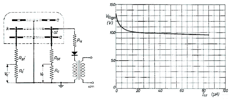
The cathode at which the auxiliary discharge is initiated can be selected by raising the voltage at the desired starter slightly above that of the others. This may be done by applying a small positive control voltage Ve across resistor Rc. The corresponding starter then reaches the ignition voltage prior to the others, so that the discharge occurs at the desired position. If the control voltage Vc is transferred to another starter the re-ignition will take place at the new starter-cathode combination at the next (half) cycle, and so on. The reason for employing an unsmoothed supply voltage will now be clear, namely that, in order to transfer the discharge from one cathode to another, the discharge must first be extinguished by reduction of the supply voltage to below the maintaining value, after which it must rise again gradually so that the desired starter can initiate the next discharge. The control voltage, that is to say the additional impulse required to initiate the auxiliary discharge at a particular cathode, may be very much smaller than the maintaining voltage, since the total starter voltage need only be slightly higher than the voltages at the other starters. A control voltage of only 5V is all that is required with the ZM550, provided the supply voltage meets certain requirements. A signal of only 5V can conveniently be supplied by a transistor circuit. If this circuit is so designed that a signal is fed to starter st1 for a count of 1, to the adjacent starter st2 for a count of 2, and so forth, the tube will indicate the result of a count. It should be recognized that it is immaterial whether the tube can follow the counting operation or not. Provided that after the completion of a count the control signal is applied to the corresponding starter, the location of the discharge initiated at the next re-ignition of the tube will correspond to the final result of the count. Since the power for the main discharge is not supplied by the control circuit, it is easy to ensure that this discharge will be sufficiently bright to provide a clear visual indication. By connecting the anode to earth, as shown in Fig. 8, one of the terminals of the transistorized control circuit can also be earthed, which greatly facilitates the circuit design. |
| to top of page | back to homepage |
I was planning to write a section here on the invention and the development of the Z550M/ZM1050 indicator tube. However, when researching the tube I came across so much interesting material that I decided to write a dedicated page on it. Click on the picture below to read more about this fascinating tube and the people who invented and developed it!
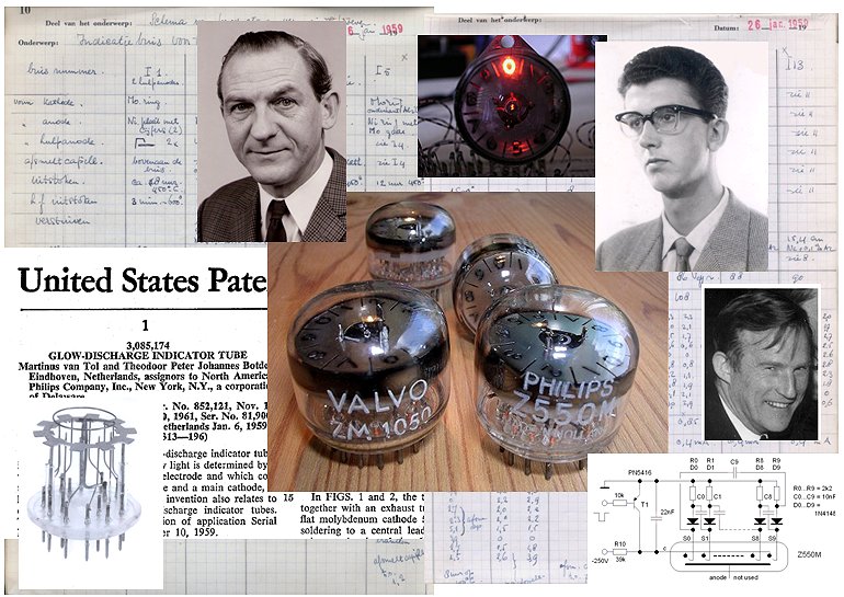
Click here or on the picture to link directly to the
“The Making of the Z550M/ZM1050” page.
| to top of page | back to homepage |
The ZM550 used as a ring counter.
A clock with ZM550 ring counters.
So stay tuned !

I would like to thank the following people for their contributions:
Mr. Philip Lentz, Ms. C.A.M.Th. van Vlodrop-Goedmakers, Mr. Wil Graat, Mr. Engel Hoefgeest and Corrie Panken and Ad Gast from Philips Research,
http://www.electricstuff.co.uk/oldbooks.html
| to top of page | back to homepage |