Both my father as well as my grand father were keen electronic hobbyists.
When I was still a very young child, my father thought me the basics of
tubes and transistors. However, the digital revolution completely passed him,
and as a consequence I also had no idea what all these strange "bell" shaped
symbols and this talk about "1"s and "0"s was all about.
This changed when the Dutch
electronics magazine "Elektuur" (in the rest of the world known as "Elector")
published, starting from April 1972, what they called "IC-kaarten" (IC-cards).
The idea was that you removed the center page from the magazine and cut it into
four pieces to obtain a card that would fit into a filing system. The front side
of each card would gave the connections to the IC, while the other side would
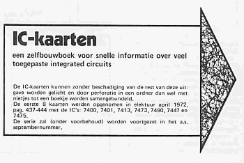
contain technical details and an application circuit. Fig. 1 depicts, as an
example, the front- and back-side of the IC-card for the 74141 nixie driver.
Figure 1. Example of an Elektuur "IC kaart" taken from June 1972 number (no. 109).
Intrigued as I was by the mysterious symbols, these cards enabled me to decipher the basic ideas behind digital electronics. And like most things in life, once you have mastered the basics, the rest comes pretty smoothly. For years I was obsessed by the possibilities of these small black building blocks. It soon became my dream to build a digital counter with display. Now you have to remember that in those days something like a seven segment display was something that not that many people, including myself, had seen in real life. So for my birthday I asked a SN7490 decade counter, a SN7447 BCD to seven-segment decoder, and a 3015-F Numitron display. In those days these components were rather expensive! In the same Elektuur magazine from which the Fig. 1 IC-card was taken, I have an advertisement which offered these components. In the table below, you will find the prices of these components as they were then in guilders, but also in the price in Euro now, based on the ratio of the prices of the Elektuur magazine then (fl 1.95) and now (Euro 6.85).
|

|
Years later my father, who worked at a Shell chemical plant, brought an old
discarded data-logger with him home from work for me. My father was in
many ways not an easy man, but he always stimulated me in everything I did,
and he was very proud of me. I owe a great deal to him, and I have many
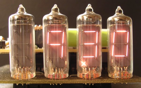
happy memories of him. Among others the data-logger contained a small PCB
with four DA2300 Numitron displays plus SN7447 seven-segment decoders (Fig. 2).
For more than twenty years I have dragged it behind me from home to home.
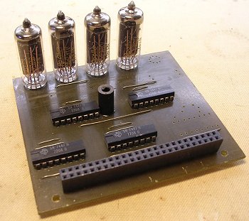
Figure 2. The PCB with the four DA2300 Numitrons from the Data-logger.
At first I thought it was a piece of old fashioned obsolete technology and I preferred to use modern LED displays instead. Later when I realized what a pretty and romantic devices they really are, I did not dare to use them, because I realized that by using these filament displays I would eventually destroy them.
At last I have an idea how I can use these tubes for a clock and still be
assured of a long life time. In my hobby shack I have one central switch
that I use to switch everything in the room on and off. If I run my clock
from that mains, the tubes will only be on only when I am actually
working there (unfortunately not that much actually). It does however
imply that the clock will need a battery backup to keep it running even
when the mains is disconnected.
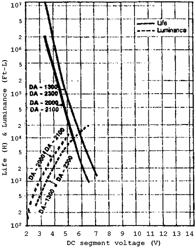
Figure 3. Life expectancy of the DA-2300 tube as a function of segment voltage. (adapted from the datasheet [1]).
On top of that I decided to reduce the supply voltage of the tubes.
Figure 3 is taken from the DA2300 datasheet [1]. It gives the life expectancy of
the tube as a function of the supply voltage. For a nominal supply voltage
of 5 V, the graph indicates a life expectancy of 100.000 hrs or 11.5 years.
We see that when the supply voltage is reduced, the life expectancy increases
exponentially. In this clock the 0.8 V voltage drop across a diode is used
to reduce the supply voltage to 4.2 V. At this voltage the displays are still
bright enough, while the life expectancy has now increased to 1000.000 hrs,
which is more than a century. This combined with the fact that the clock
will only be switched on for at most a few hours a day, will hopefully make
that the displays will last forever.
The principle of battery back-up is explained in Fig. 4. The supply voltage
for the circuit is divided into two categories. Components that only need
to be powered when the clock is connected to the mains, like the numitrons,
the SN7447 decoders and the shift registers are connected to Vcc. Components
that need to be powered continuously, in this case only the processor,
are connected to Vback.
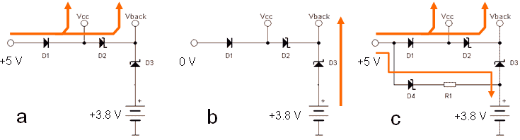
Figure 4. Principle of battery back-up, a. mains connected, b. mains disconnected battery back-up, c. mains connected with battery recharge.
Figure 4a depicts the situation when the circuit is connected to the mains.
In this case the mains fed +5 V supply is present. The Vcc supply is now
switched on via diode D1. The diode causes a voltage drop of ca. 0.8 V so that
Vcc=4.2 V (see above). Diodes D2 and D3 form a logical "or" circuit.
Which diode is conducting depends on whether Vcc is higher or lower than the
battery voltage. When the mains is on, Vcc will usually be higher than the
battery voltage so D2 will be conducting while D3 is blocking.
 Vback is now fed by
the mains supply. The reason that for D2 and D3 Schottky diodes have been used
is that in forward bias, the voltage drop over these diodes is only 0.2 V.
If normal diodes would have been used, the difference in the logical
"high" level would be 0.8 V. In this way this difference is minimized.
Instead of the "European" BAT83 any suitable small-signal schottky
diode may be used.
Vback is now fed by
the mains supply. The reason that for D2 and D3 Schottky diodes have been used
is that in forward bias, the voltage drop over these diodes is only 0.2 V.
If normal diodes would have been used, the difference in the logical
"high" level would be 0.8 V. In this way this difference is minimized.
Instead of the "European" BAT83 any suitable small-signal schottky
diode may be used.
When the mains is switched off (Fig. 4b) Vcc drops to zero. In this case diode
D3 will conduct, and Vback is now supplied by the battery. Diode D4 and
resistor R1 bypass the "or" circuit and take care of the charging of the
battery when the mains is on. When the +5 V supply is present, D4 will conduct
and charge the battery with a current given by (5-0.2-Vbat)/R1. For R1=47 ohms
and Vbat=3.8V this amounts to 21 mA. For a 660 mAhr battery this may be
considered as trickle charging, which may be applied to the battery
continuously. Note also that the charge current is in a certain sense "self
regulating" since the charge current will automatically decrease when the
battery voltage increases. Again a Schottky diode is used because of the low
voltage drop. The voltage drop of a normal diode would leave only a very
small voltage margin for setting the charge current with any reasonable
accuracy.
The full circuit diagram is given in Fig. 5. Figure 5 only serves to give an
overview of the circuit. By clicking on the figure a detailed pdf file
can be downloaded and printed. In the lower left corner we find the battery
back-up circuit discussed in the previous section. A number of jumper
switches has been added to the circuit. Jumper 1, which is normally open,
can be placed to increase the supply voltage if desired from 4.2 V to 5 V.
This will increase the brightness of the tubes somewhat, but will reduce
their life expectancy. By removing jumper 2 the trickle charging of the
battery can be switched of. By removing jumper 3 the battery back-up can
be switched off all together.
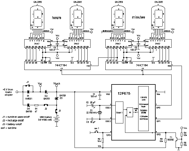
Figure 5 Circuit diagram of the Numitron clock.
(click on the image to download a detailed pdf file)
Four very traditional SN7447 "BCD to seven-segment decoder/drivers" are used
to drive the Numitron tubes. They were already present on the PCB which
holds the Numitron tubes. Like the SN74141 Nixie driver, the SN7447 is also
starting to become a collectors item. I knew of the existence of SN74LS47
types, but until recently I had never seen them.
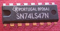 Then in a discarded stock of old
TTL ICs there they suddenly where, so they really exist!
Then in a discarded stock of old
TTL ICs there they suddenly where, so they really exist!
In the Nixie II clock, I for the first time used shift registers to drive the display decoders. The processor outputs the time in serial BCD format and clocks the data into a shift register to convert it to parallel format again. The advantage is that only two I/Os of the processor are used. An additional advantage is that in this way the shift registers can be placed close to the decoders. So the traditional "star shaped" interconnect pattern between the processors and the decoders is replaced by a "chain shape". In this way the amount of wirering is minimized. Unlike the HEF4096 shift registers used in the NIXIE II clock the 74HCT164 does not have an output latch. This means that during shifting of the data, random data appears at the outputs, which could result in display artifacts. As it turned out, the shifting of the data is so fast compared to the on/off time of the Numitrons and the response time of the eye, that this was no problem. The order in which the outputs of the shift register are connected to the decoders looks somewhat strange. This was just the easiest way with the least number of wires crossing. A look-up table in the program of the processor takes care of translating the time to the proper output code.
As will be explained in the next section, the processor is in sleep mode during most of the time to reduce the power consumption as much as possible. In order to detect in sleep mode when the power is switched on again, I/O GP2 has been programmed to wake the processor when a change on this input occurs. The simple circuit around T1 generates this signal. As long as Vcc=0 V, T1 will be switched off and R3 will pull GP2 high (Vback). When the mains is switched on again, Vcc will become 4.2 V and T1 will be switched on. This will pull GP2 low. I did not want to connect GP2 directly (or via a resistor) to Vcc since in general Vcc > Vback.
The next section will explain how a 32.675 KHz crystal is used to keep
track of the time. The crystal came from an old battery alarm clock.
In the 12F675 datasheet, Microchip recommends two 68-100 pF
capacitors for C2 and C3.
When I first tried the clock with two fixed 68 pF capacitors, I found that
the clock was behind by 4 seconds a day. I then replaced C2 and C3
by two 33 pF capacitors. The clock was now 2 seconds ahead of time each day.
By replacing C2 with a 15-50 pF trimmer capacitor it is now
possible to adjust the frequency for maximum accuracy.
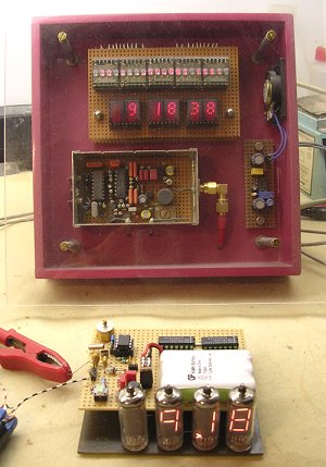
Figure 6 Calibrating the time base against my DCF77 reference clock.
Some years ago I fabricated a "DCF77" radio clock. DCF77 is a long wave time signal and standard-frequency radio station. Its primary and backup transmitter are located in Mainflingen, about 25 km south-east of Frankfurt, Germany [2,3]. DCF77 has been in service as a standard-frequency station since 1959; date and time information was added in 1973. The 77.5 kHz carrier signal is generated from local atomic clocks that are linked with the German master clocks in Braunschweig. The 50 kW strong transmitter can be received in large parts of Europe, as far as 2000 km from Frankfurt. Its signal carries an amplitude-modulated, pulse-width coded 1 bit/s data signal [4]. Due to the excellent receiver of the clock (a description on these pages is planned), the clock usually has a reception quality in excess of 99%, meaning that the clock is continuously synchronized with the DCF77 in Germany. It is always handy to have the absolute time available in house! I used the DCF77 reference clock to calibrate the time base of the Numitron clock (Fig. 6). With some patience it appeared possible to bring the average error down to less than one second per day.
The circuit was built on a piece of breadboard (Fig 7).
The use of the shift registers keeps the circuit simple with minimal wirering.
The battery is a Nickel-Metal Hydride battery from an old cordless phone.
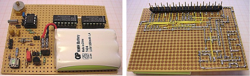
Figure 7 Front- and back-side of the clock PCB.
The 12F675 has some very nice features that make it particularly attractive for these kind of low power time keeping applications. Normally in a program for a clock like this, the processor is more than 99% of the time idle. Most of the time it will be checking some kind of flag to see if another second has passed, or the input to see if a key was pressed. Even for these simple tasks, the processor will consume maximum power. The so called sleep mode was invented to overcome this dilemma. After execution of the SLEEP instruction, the processor will switch most of its components off, until an event occurs that will wake it up. Which components are switched off during sleep, is selected by setting the proper control bits before executing the SLEEP instruction. After the processor has "woken up", it continues by executing the next instruction after the SLEEP instruction. The processor at this point knows that, since it has "woken up", an event must have occurred. By checking the various flags and bits, it can sort out what the origin was of the event.
The programmer has the possibility to select the cause of wake-up from a
whole range of sources. This is done by using the processor's
interrupt logic infrastructure (Fig. 8). Observe that when the global
interrupt enable flag (GIE) is disabled, the same conditions that will
otherwise generate an interrupt, will now wake-up the processor. In this clock
both a timer1 roll-over condition, and a change of the input signals on I/O
GP2 (power down) and GP3 (key) are used to wake-up the processor from
sleep mode.
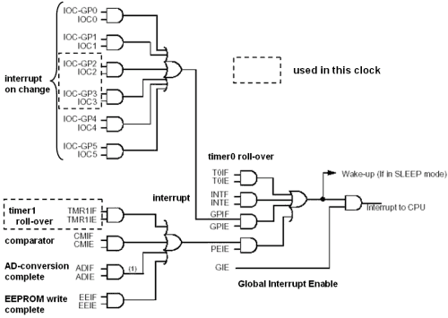
Figure 8 The interrupt logic structure of the 12f675 is used to select the wake-up source. In this clock only the timer1 roll-over and the GP2 and GP3 "interrupt-on-change� are used.
When the processor is programmed (by setting the proper bits in the CONFIG register) to run on the internal 4 MHz clock, the oscillator circuit can be configured to serve as a clock source for timer1. The oscillator runs in Low Power 32.768 kHz Crystal mode in this case. The 32.768 kHz signal is first devided by two by the programmable Timer1 Prescaler. So the input frequency of the 16 bit timer1 is 16.384 kHz. When the timer has counted to 65.536 (all 1s) it rolls-over to zero which causes the TMR1IF flag to be set, resulting in a wake-up of the processor. So in this way the processor wakes-up every four seconds. A software counter counts these four second "wake-up calls" and after 15 calls increments the minutes.
Each of the GPIO pins is individually configurable as an interrupt-on-change pin. For and enabled interrupt-on-change pin, the momentary value of the pin is compared with the old value latched on the last read of GPIO. The compared values of the I/O pins are or'd together to set the GP Port Change interrupt flag bit (GPIF) in the INTCON register. This "interrupt" can be used to wake the processor from sleep. In this clock only GP2 and GP3 have been used in this mode. A 0 -> 1 transition on GP2 indicates that the mains was disconnected. A 1 -> 0 transition indicates that the mains was switched on again. A 1 -> 0 transition on GP3 is caused by pressing the key, a 0 -> 1 indicates the key is released.
On wake-up the main program calls routine WAKE_UP. The first thing this routine does is to do a dummy read to the I/O's to remove a possible input mismatch condition followed by resetting (set or not) of the GP Port Change Interrupt Flag (GPIF). Next the routine checks to see if there was a timer1 roll-over (TMR1IF=1). If so TMR1IF is cleared and the time is adjusted. Next the routine checks if the clock is connected to the mains or not. If it is, the key is checked first. If is is pressed, the clock re-boots. If it is not pressed, the present time is shifted into the display shift registers and an interrupt-on-change from the key (GP3) is enabled. If the clock is not connected to the mains, the outputs are made low and an interrupt-on-change from the key is disabled. Perhaps you prefer to have this piece of prose in a pseudo programming language:
- dummy read to I/O's to remove a possible mismatch condition
- clear the GP Port Change Interrupt Flag (GPIF) whether it was set or not
IF there is a timer1 roll-over (TMR1IF=1) THEN
   - clear TMR1IF flag
   - adjust time
ENDIF
IF clock connected to the mains THEN
   IF the key is pressed THEN
      - re-boot the clock
   ELSE
      - shift present time in display registers
      - enable interrupt on change from key (GP3)
   ENDIF
ELSE
   - make outputs low
   - disable interrupt on change from the key (GP3)
ENDIF
Observe that we do not allow the processor to be woken by pressing the key
when the mains is disconnected. After these actions, the processor returns to
sleep mode again, waiting for the next wake-up (program listing at label:
main_9).
During the writing of the program, I made a number of stupid mistakes, which
cost me a lot of time. In one of the trial versions of the program, I observed
that sometimes, so not all the time, the current consumption during battery
back-up was unexpectedly high (ca. 15 mA). My first thought was that the
processor was not a sleep. But in that case why should the current be higher
than in normal mode ? Sometimes the unexpected high sleep current would drop
to 10 µA, the normal current that one would expect during sleep mode.
After a while the current would then jump up again to 15 mA. By switching the
clock on and off I observed that the high sleep current only occurred when the
least significant digit of the minutes was a 1,3,5,7 or 9. This quickly gave a
clue to the origin of the problem. For these digits the last bit that was
shifted in the shift register is a "1". What happened was that the routine that
shifts the data into the register did not reset the output bit to zero but left
it high. Now, every IC has at its pins what is called an Electro Static
Discharge Protection (ESD) circuit. This circuit, amongst others, consists of
two diodes, which clamp the pin voltage to the supply pins. This means that
the internal voltage in the IC can never raise above Vcc or below Gnd. So
when during backup Vcc drop to zero, the protection diode starts to conduct
to protect the IC (Fig. 9). This will draw the maximum current from the
PIC's I/O pin. A small program modification removed the problem.
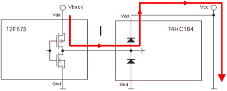
Figure 9 Current flowing from a "high" output pin of the processor during back-up through the ESD protection diodes of the next circuit.
The second problem was also a bit of a puzzle and related to the way I program
the PIC. I have a separate programmer and in order to burn a new program
in the PIC, I remove it from the application, and insert it into the
programmer (Both have a ZIF socket). When I develop a program for an
application like this, I usually start very simple to test the hardware etc.
I then increase the complexity step by step, debugging every addition on the
way. At a certain point when I introduced the sleep part of the program, the
clock started to show some very strange behavior. To cut a long story short
what happened was: I left jumper J3 in place all the time. This meant that when
I return the PIC from the processor in the clock, the PIC is powered up
immediately when I insert it in the second. I did not notice it of course,
because the displays are off. A small thing, which puzzled me for hours.
But great is the satisfaction when you finally discover what the fault was!
Obviously I wanted to know the power consumption of the clock (or in other words the processor) during backup. By replacing jumper J3 with an Amp meter it appeared that the sleep standby amounted to ca. 10 µA. A little bit more than the datasheet predicted, but low enough for me. However, the question remained whether the additional power the processor consumes during the short intervals it is awake contributes significantly to the overall power consumption.
To get an answer to this question, I placed a 330 ohm resistor in series with the the Vdd pin of the 12F675, without any decoupling capacitor at the Vdd pin. The voltage drop accross the resistor is now a direct measure of the current (0.33 V per mA). On paper this is a horrific thing to do. Normally one would take every precaution (decoupling caps. low inductance wiring etc.) to minimize voltage transients at the supply pin as much as possible. But anyhow the processor didn't appear to mind it much, and still functioned flawlessly.
Normally the processor wakes up only once every four seconds. Unfortunately
I do not posses a memory scope, so in order to observe the wake-up event on a
normal scope, I modified the program so that Timer1 reloads with FF80H after
every wake-up. Timer1 now rolls over after 128 counts so that a wake-up
is generated every (2*128)/32768= 7.8 ms.
The result is now a nice and stable picture on the scope, and a clock running
like hell.
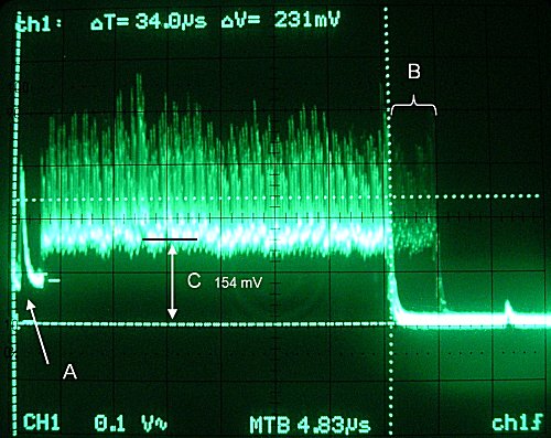
Figure 10 Current consumption during a wake-up event. The measured voltage is the voltage drop accross a 330 ohm resistor placed in series with the Vdd pin.
Figure 10 depicts the voltage drop over the 330 ohm resistor. So 0.33V corresponds to 1 mA current. We first observe that most of the wake-up's take about 34 µs. Sometimes a wake-up is a little bit longer (marked B in Fig. 10). This caused by the fact that every fifteenth wake-up the processor increments the minutes and if needed the hours (15*4=60 seconds), this of course take a little more time. When the processor wakes-up it first starts the internal oscillator and then waits until it is stabilized. According to the datasheet this takes about 3 µs, nicely corresponding to A period in Fig. 10. The current during normal operation shows large transients. These are obviously caused by the fact that different instructions and actions inside the processor activate different parts of the processor. Normally a decoupling capacitor would be used to equalize these transients. If we assume that the average current consumption is there were the scope image is brightest (B in Fig. 10), then the average current during wake-up is 0.154/330 = 0.47 mA.
The ratio of active to sleep time is 34e-6/4=8.5E-6. By multiplying this with the current during wake-up, we find the average current that these wake-up periods add to the overall current consumption: 8.5E-6*0.5 mA = 4.25 nA! Negligible compared to the total current.
The ratio of the battery charge current to the average current use is about 10mA/10µA=1000. This means the clock should be connected to the mains for at least an hour every 1000 hour, say one hour every month.
In the absence of battery self-discharging, the clock would run for about
seven years on a fully charged battery. However, although these
NiMH batteries are supposed to suffer
less from "memory effects" than NiCd's, I still think it is better for
the battery to be charged and de-charged on a regular basis.
For this reason I think I will shunt the battery with a resistor to
"give it something to do". A 47 kohm resistor will increase the
current consumption to ca. 100 µA. This would require an average
on-time of ca. one hour every hundred hours.
The compressed file which can be downloaded here , contains the following files: