|
|
I have two sons Geert (10) and Daan (8). Daan is not a sportsman at all. Like his father, he prefers to play with construction toys like LEGO TECHNICS and KNEX and with the PC. He often joins me in my electronics shack, and I have to say that he has a better hand in soldering than many of my colleagues. Geert on the other hand has a totally different personality. Rain, wind, snow, no matter what weather it is, he is only really in his element out of doors. Like his mother he has no liking for any precise or delicate tasks, the rougher the better!
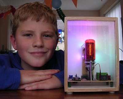
To my surprise it was Geert who first asked me to make him his own NIXIE clock. Knowing Geert I knew that it had to be a special clock. It took me quite some time to come up with an original idea. One thing was clear however, I happened to have in my NIXIE collection a single beautiful giant ZM1042 (for the record, I got it from Jim Oostveen). For me it was obvious that a single digit NIXIE clock built around this tube would be just the thing for Geert. Some time ago, while visiting our local IKEA store, I found just the perfect case for the clock: a 14x19x8 cm wooden frame with a glass window front and a white hardboard back. It was just after I made the random color design for Jan Verhoevens farewell present, and it seemed a nice idea to combine the single tube NIXIE clock with an ambient light feature. Personally I am completely mystified by the success of the Philips "ambi-light LCD" TV. I work at Philips Research myself, and I would never have believed that somebody would pay extra money for a TV that projects a colorful aura on the wall behind the TV, but the fact is there. Also the positive reactions I got on Jan Verhoevens color changing farewell clock, let me to the conclusion that colors are very important to people. I myself am totally color blind, so unfortunately I will never be able to appreciate this. But, Geert is not color blind, and he thought it was a great idea!
For some time now I have been playing around with the idea to make a clock in which the high
voltage for the NIXIE tubes is derived directly from the mains, without the need for an high voltage
transformer or switch-mode power supply. Since there was only very little space in the wooden
case that I had in mind for this clock, I decided to use it for Geert's clock. Connecting a clock
directly to the mains requires some special precautions, which will be explained in one of the
next sections.
To make the clock even more interesting I wanted to make the digits in the NIXIE tube to fade
slowly on and off. Especially for these giant NIXIE tubes the effect is very striking. It looks as if
the digits are gas lit!
In a circuit which is directly fed from the mains, the circuit is connected via a direct galvanic
connection to the mains. Before I start with the description of the clock circuit, I have to
explain why directly mains fed circuits are so dangerous, much more dangerous than circuits
that use the same high voltage but derived from a transformer.
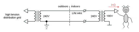
Figure 1 Touching a high voltage circuit that is isolated from the mains
is not dangerous as long as no current can flow.
Figure 1 shows a simplified schematic drawing of the final part of the power distribution grid
that delivers the power to your home, connected to an appliance that uses a transformer.
Lets for the sake of this example assume that it is a 240V to 180V transformer used to
feed the NIXIE tubes.
In the last distribution station the high voltage from
the power grid is transformed down to e.g. 240V, the mains voltage we have in Europe.
The power is delivered through two wires. One of these wires is called the "life wire" or the
"phase wire". The return wire is called the "null" or "ground" wire. It is important to note
that at the distribution station the ground wire is connected to ground, that is the
ground that you are standing on!
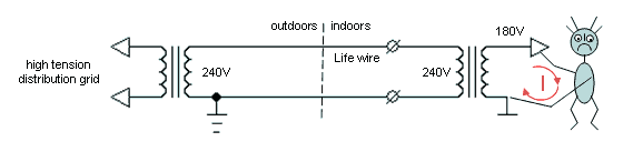
Figure 2 Touching an high voltage circuit at two points closes the loop so that
a current can flow,
resulting in a painful if not lethal shock.
When any part of the circuit at the secondary side of the transformer is accidentally touched,
nothing happens since there is no path for the current to flow to ground. The entire circuit is,
although it carries high potential differences, floating with respect to ground. The situation
changes dramatically when accidentally two points in the circuit are touched (Fig. 2).
A large voltage between the points touched will give you a nasty shock or may possibly even kill you!
This is the reason why my father thought me always to keep one hand in my pocket while fiddling
around with high voltage circuits.
The fact that the secondary side of the transformer is floating with respect to the mains
grid, makes that we can define one of the two terminals as ground and connect it e.g. to the
cassis. In this case we only need to worry about isolating the high voltage derived from the other
transformer terminal.

Figure 3 In a circuit that is not isolated from the mains, even a single touch will
result in a flow of current through the ground you are standing !
When no transformer is used, the circuit will always carry a deathly potential with respect to the real ground (Fig. 3). In this case a single touch to any part of the circuit will result in the flow of a current straight though your body to ground. This may very easily kill you! Note that in this case we have no way of knowing which terminal is connected to the live wire and which terminal is connected to the ground since this will depend on the position of the mains plug in the wall outlet. Consequently, we have no way of defining one of the terminals as a local ground. The only solution is to isolate the entire circuit!
It is good for a moment to think of what this really means. It means that you have to treat every part of the circuit as if it is connected to a lethal voltage with respect to ground, even if the potential differences in the circuit are only small! This is sometimes a little bit difficult for people to understand. I used to have a neighbor who was in the habit of decorating his garden with Christmas tree lights. Now, instead of buying decent outdoor type of lights he used cheap indoor lights. Being a "they don't fool me" type of man he argued: I have 40 lights running on 240V so every light only runs on 240/40=6V, which is not dangerous at all. Despite my repeated arguments, he was unable to see that although the potential difference across each lamp might be as small as 6V, the potential difference with respect to ground can be as high as 240V. In other words lethal.
The idea of feeding a circuit directly from the mains is actually very old. The first radios operated on batteries, one for the filaments and another high voltage battery for the plates (anodes). The obvious reason was that only few houses were connected to the mains! Since the current drawn from the anode batteries was usually very small, in the order of mA's, these batteries only needed replacing every few months or so. Nevertheless is was cumbersome and expensive. In the forties almost every body became connected to the mains, so mains fed power supplies (with transformer) began to replace batteries. Directly after the war everybody wanted a radio for an affordable price, so radio set makers were forced to cut down production costs. One of the most expensive parts in a radio was the mains transformer. Set makers came up with a clever trick to eliminate the transformer. Instead of making tubes that would run on a filament voltage of 4 or 6 Volts, they fabricated tubes with a much higher filament voltage so that when the filaments of all the tubes in a radio were placed in series, they could be directly connected to the mains. An example of such a radio is the 209U from Philips ( click here to view the schematics ). Often tube manufacturers would design a set of tubes which together would make a complete radio while the filaments in series could be connected to the mains. Such a set of tubes was called a "line up", a term still in use today for e.g. a set of transistors that will make an RF power amplifier. The same system was adopted for televisions. As explained, a consequence was that the whole cassis of the set was inevitably connected to the mains, and had to be completely isolated. The system was first abandoned for radios. Especially high end radios were provided with a gramophone and tape recorder input. These inputs needed a ground connection, so that isolation from the mains by means of a transformer was unavoidable. For television the directly mains fed principle was maintained however throughout the whole tube area. In most modern televisions the high voltage flyback converter transformer plays the double role of isolating power supply and high voltage converter.
Finally a personal anecdote to end this section. When I was in high school, it must have been around
1976, I built my first what was then called "Video Display Unit".
 It was an interface for my SC/MP
microcomputer to display characters on a normal television screen. There was very little money
those days, so almost the complete circuit was built up from old parts and dump stuff. No regrets
though because it is great to make something from virtually nothing, and I learned a lot from it!
Of course there was no money for a really video monitor, those things were terrible expensive
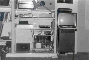
those days anyway. Instead I used an old 17TX250 television from Philips (see picture on the right).
The video signal was directly
connected to the grid of the video amplifier tube. To make it work, obviously the ground of my
computer system had to be connected to the ground (chassis) of the TV. But as explained, the
chassis was connected to one of the pins of the mains plug! When this pin was connected to the
ground wire everything was relatively ok. However, when accidentally that pin was connected
to the life-wire, my complete microcomputer would be connected to the lethal mains voltage!
A color code system was used to make sure that I would never make this fatal mistake.
Thinking back the whole affair was incredibly dangerous and it was a wonder that my father
let me do it. Never ever try to do something yourself.
It was an interface for my SC/MP
microcomputer to display characters on a normal television screen. There was very little money
those days, so almost the complete circuit was built up from old parts and dump stuff. No regrets
though because it is great to make something from virtually nothing, and I learned a lot from it!
Of course there was no money for a really video monitor, those things were terrible expensive
those days anyway. Instead I used an old 17TX250 television from Philips (see picture on the right).
The video signal was directly
connected to the grid of the video amplifier tube. To make it work, obviously the ground of my
computer system had to be connected to the ground (chassis) of the TV. But as explained, the
chassis was connected to one of the pins of the mains plug! When this pin was connected to the
ground wire everything was relatively ok. However, when accidentally that pin was connected
to the life-wire, my complete microcomputer would be connected to the lethal mains voltage!
A color code system was used to make sure that I would never make this fatal mistake.
Thinking back the whole affair was incredibly dangerous and it was a wonder that my father
let me do it. Never ever try to do something yourself.
From the previous section it should be clear that circuits directly fed from the mains
are in principle fine, as long as special precautions are taken for the isolation of the complete
circuit. Special 220V to 220V transformers are ideally suitable for this, but I don't have one.
Instead I use two "low-voltage" transformers back-to-back (Fig. 4a). Transformer T1 is a rather
bulky 10V/4A transformer, T2 is a much smaller 7V/0.7A type. The mismatch
between T1 (10V) and T2 (7v) is explained by considering the resistive losses in T2.
T2 is designed so that it delivers 7V under nominal load conditions. Under nominal conditions
the resistive losses cause a considerable voltage drop in both the primary and secundary
windings of the transformer. The manufacturer of the transformer
added secundary windings to compensate for these losses, so despite the 220V/7V specification,
it really is a 220V/10V transformer (Fig. 4b).
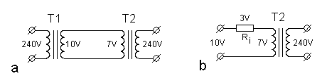
Figure 4 Isolation of a circuit from the mains is ideally done with a special
240/240 (or 110/110) isolation transformer.
By placing two normal transformers
back-to-back the same result is archived (Fig. 4a).
Due to voltage drops across the windings (Fig. 4b)
it may me necessary to use transformers with different secondary voltages.
In the introduction I mentioned that instead of switching the NIXIE digits simply on and off, I wanted to slowly fade them on and off. This means that one way or the other we need to have a means of varying the intensity of the digits between zero and maximum. With a gas discharge device this is not so easy as with a simple incandescent lamp. A NIXIE tube ignites at a voltage of ca. 180V, and from that point on the intensity is only weakly dependant on the current. The best way to dim a NIXIE tube is to use a simple pulse-width modulation scheme. This means that the tube is switched on and off at a pace fast enough so that the eye perceives it as continues. The brightness is now directly proportional to the on/off duty-cycle. However, this only works if the tubes are fed from a nice stable (ripple free) DC voltage.
At first I had the idea to use a standard bridge rectifier followed by a storage capacitor to
decrease the ripple on the high voltage. At second thought this appeared not to be a good idea for
at least three reasons. In the first place these high voltage capacitors tend to wear down
and breakdown eventually. Secondly, the capacitor would just be too big for the printed circuit
board I had in mind. The last reason is more subtle. Unless the storage capacitor is very large,
we will still end up with a certain amount of ripple on the high voltage. This ripple will
cause interference with the pulse-width modulation scheme resulting in unwanted
modulation of the brightness of the digits at the beat frequency. So the pulse-width modulation
has to be synchronous to the mains frequency. This is of course a technique well known from
all standard light dimmers and is called phase-cutting. In this case no high voltage capacitor is needed
at all.
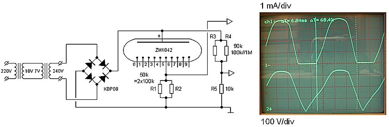
Figure 5 Test circuit to study the current-voltage relation of the ZM1042 when
it is driven by double-sided rectified AC voltage.
Before going into more detail on dimming nixies with phase cutting, I built a simple test circuit
(Fig. 5) to get a better feeling for the operation of nixie tubes when they are fed with a full-wave
rectified signal. Two standard low voltage transformers back-to-back are used to isolate the circuit
from the main. In this case the current limiting resistor R1//R2 was placed at the cathode side
of the tube. The voltage across this resistors is a direct measure for the cathode current. A voltage
1 V corresponds to 1/50000=20 µA. Resistors R3-R5 form a simple 1:10 voltage divide to reduce
the voltage at input of my the oscilloscope input. The lower trace represents full-wave rectified
220V voltage accross the tube plus load resistor. When the tube ignites (indicated by the
left dashed line)
the current drawn by the tube causes a voltage drop over the series resistances in the transformers.
This causes the distortion of the sine wave signal. The ignition voltage is ca. 160V and the extinguishing
voltage is slightly less. Each half-wave period of 10 ms the tube is on for 6.8 ms. The peak
current with the 50kohm load resistor is about 4.2 mA which is the maximum current specified
in the datasheet. The average current measured with an old analog multimeter was slightly less than
2 mA.
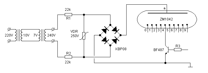
Figure 6 Principle of the pulse-width modulation circuit used to control the brightness
of the NIXIE tube in this clock.
Figure 6 depicts the basic circuit diagram of the phase-cutting circuit. The current is switched
on and off by a BF487. The BVceo of the BF487 is 400V. The base of the transistor is
driven by a control circuit which operates in phase with the power-supply voltage.
The raw mains voltage is polluted with high voltage transients and spikes caused by
the on and off switching of heavy (inductive) loads. The low-pass behavior of a mains
transformer normally to a large extend removes these high frequency components.
When no mains transformer is used, special precautions are needed to remove these
high voltage spikes. A simple way to do this is shunt the spikes with a Voltage Dependent
Resistor (VDR). A voltage depended resistor is a device which at voltages below a
certain breakdown exhibits an almost infinite resistance. When the voltage increases beyond
a certain value the resistance decreases dramatically. Figure 7 shows the I-V curve
of a VDR specified for 230V AC, measured on a curve tracer. The maximum peak-peak value of
an AC voltage with an RMS value of 230 V is SQRT(2)*230V=325V. To compensate for variations
in the mains voltage and manufacturing tolerances the manufacturer of this VDR device selected
a breakdown voltage of 400V. Normally the VDR has to absorb all the power in the transient itself.
In this clock a trick was used to make life for the VDR a bit easier. Since only one tube
is used, the current limit resistor which is normally placed in series with the anode, could now
be shifted in front of the rectifier. For symmetry the single 47 kohm resistor is split into
two 22 kohm resistors. The VDR is placed behind these resistors so that most of the power in the
transient is absorbed in the resistors. For the resistors 5 Watt types have been used so that
when in case of a calamity e.g. the rectifier short circuits, the resistors can easily carry the
short circuit current.
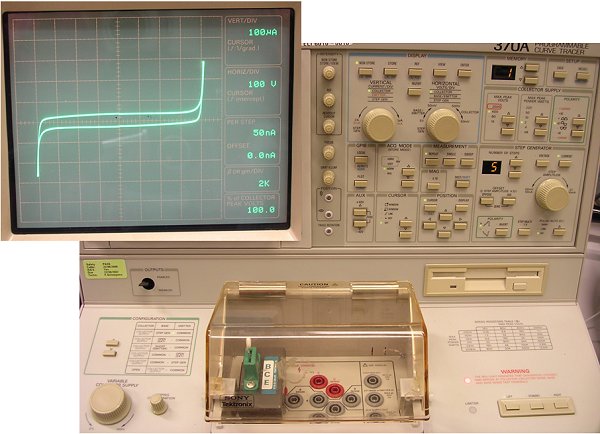
Figure 7 I-V curve of a VDR rated at 250V AC measured on a Tektronix 370A curve tracer.
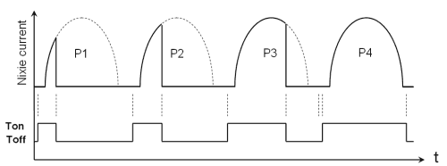
Figure 8 Principle of phase-cutting, a form of synchronous pulse-width modulation for AC signals.
I wanted to test my ideas for the NIXIE dimmer first before building the final clock.
Figure 9 depicts the circuit diagram of the test circuit. The circuit basically consists
of three blocks: the power supply, the controller and the tube with switching transistor.
The high voltage part of the power supply is identical to the circuit of Fig. 6. For the
low voltage power supply I used a very small 220V to 6V/0.11A transformer I had lying around.
After rectification this will result in a DC voltage of ca. 7.5V. The 7.5V is a bit
on the low side for a standard 78L05 regulator to work reliable. That is why I used a supply
voltage of 4V. This is perfect for the controller, and it gives a bit more
"head-room" for the voltage regulator. For the regulator a LM317K is used.
The LM317 always tries to adjust the output to such a value that the voltage between
the output and the adjust input is held constant at 1.25 Volt. If we assume that the current
drawn by the adjust input is negligible, then the current through R3 and R4 is given by
I = 1.25/R4. So the voltage drop over R3 is R3*(1.25/R4). This makes the output voltage
Vout = 1.25 + R3*(1.25/R4) = 1.25*(1+R3/R4). In practice the current through R3 and R4
should be kept at approximately 5-10 mA. This sets R4 to a value between 120 and 240 ohm.
If we make R4 = 220 ohm then R3 = 176*Vout-220.
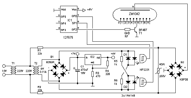
Figure 9 NIXIE dimmer test circuit.
On my NIXIE 1 clock page,
I explained why I prefer to use the mains frequency as
reference for the time. On that page you will also find the "standard" circuit I
normally use for the time base.
It basically consists of an opto-coupler, flip-flop and one-shot noise filter.
In some clocks
the one-shot noise filter is implemented in software. Since I had only very little space on the PCB
for this clock also the flip-flop was implemented in software at the expense of one additional I/O pin.
So every odd half-period GPIO0 becomes high and every even half-period
GPIO1 becomes high.
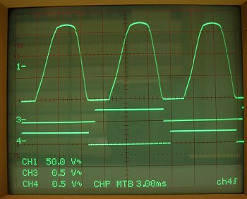
Figure 10 Output of the opto-couplers compared to the current through the tube.
Figure 10 shows the current through the tube (upper trace) and the two outputs of the opto-couplers
(middle and lower traces). Note that the two clock phases are non-overlapping due to the 1.4 V
threshold voltage of the LEDs in the opto couplers. Figure 11 shows the test circuit in action.
Only one digit is needed to test the principle. The circuit is fed by a 10V transformer not
shown in this photograph. T2 transforms this voltage into 240V followed by T3 that produces the
6 V supply voltage for the ICs. The KBP08 bridge rectifier is specified for a reverse bias of
800 V (I checked it!). The circuit is very simple, the real work is done by the software!
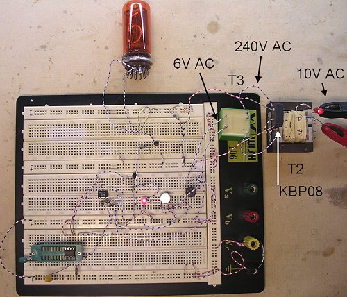
Figure 11 The dimmer test circuit on breadboard.
It is the task of the dimmer software to fade a digit on and off within a second. As mentioned in the introduction, this clock uses the "ambient light" feature that was developed for Jan Verhoevens farewell present. The LEDs for the ambient light feature are controlled by a subroutine that is called every 100µs from the main program. In order to able to merge this routine with the dimmer software, this structure is maintained for the dimmer. The dimmer is implemented by three subroutines which are executed every 100µs: "flip-flop", "phase" and "dimmer".
The "flip-flop" routine emulates the NAND set-reset flip-flop that I normally implement
in hardware. The flip-flop is set (bit "FF"=1) when GPIO1=1 and reset ("FF"=0) when GPIO=1.
Additionally the "SYNC" bit is set on every change of "FF". So "SYNC" is set at the beginning
of every half-wave period. Note that in the final program the "SYNC" bit was renamed "SYNK"
since the variable "SYNC" was already used by the 16F876 processor.
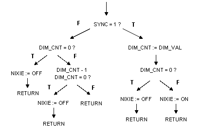
Figure 12 Flow diagram of the routine that performs the phase cutting "phase".
It is the "SYNC" flag that signals the "phase" routine that a new half-wave period
has begun. It is this routine which actually cuts the phase of the half-wave
rectified mains voltage
and thus dims the NIXIE tube. Since a half-wave period lasts (1/50Hz)/2=10ms, and the
"phase" routine is called every 100µs,
the routine is called 10ms/100µs=100 times every half-wave period.
The phase angle is measured by simply counting the number of calls to "phase".
At the beginning of a new half-wave period (signaled by "SYNC" becoming true),
the tube is switched on and counter "DIM_CNT" is cleared (Fig. 12). Every subsequent call
to "phase" "DIM_CNT" is incremented. When "DIM_CNT" equals "DIM_VAL" the tube is switched
off again. So the variable "DIM_VAL" determines the phase angle at which the tube is switched
off and thus the intensity: "DIM_VAL"=0 is tube off, "DIM_VAL"=100 tube maximal on.
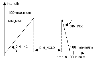
Figure 13 Definition of the parameters that control the on- and off-fading of the NIXIE tube.
Routine "dimmer" takes care of the actual fading of the tube. Like routine "phase"
it is called every 100µs. Every call the routine checks the "SYNC" bit.
Every time "SYNC" was set, the routine resets "SYNC" and adjusts "DIM_VAL" so that
the intensity of the tube is adjusted. Note that every second "SYNC" is set
one hundred times. This process is controlled by four parameters: "DIM_INC", "DIM_MAX",
"DIM_HOLD" and "DIM_DEC". Figure 13 explains the meaning of these parameters.
Parameters "DIM_INC" and "DIM_MAX" determine the fading-on of the tube. "DIM_INC"
is the value used to increment "DIM_VAL" every "SYNC". The higher "DIM_INC", the
faster the tube fades on. The incrementation of "DIM_VAL" stops when "DIM_VAL">="DIM_MAX".
So "DIM_MAX" determines the maximum intensity of the tube. Next, the intensity is held
constant for "DIM_HOLD" "SYNC"s. After this "DIM_VAL" is decreased at a rate of "DIM_DEC"
every "SYNC" until it reaches zero. It is the responsibility of the programmer to make sure
that "DIM_MAX"=<100 and that "DIM_VAL" returns to zero before the second is over.
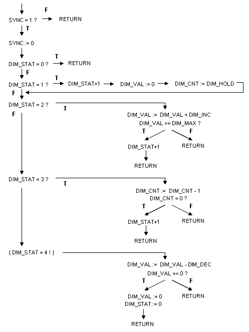
Figure 14 Flow diagram of the "dimmer" routine which controls the on- and off-fading of the digits.
The total circuit of the clock is rather straightforward (Fig. 15).
The power supply and the
clock circuit is directly copied from the test circuit described above. The LED
circuit is identical to the circuit used for the farewell present of Jan Verhoeven.
Instead of using a standard 74141 NIXIE driver I used ten high-voltage npn transistors.
The BF487 transistors have a BVceo of 400V. The primary reason why I used discrete
transistors instead of a 74141 was that the transistors have a negligible power consumption
(only a base current), while a 74141 can consume up to 100 mA. This is too high for
the small transformer and the LM714K regulator I had in mind for the clock.
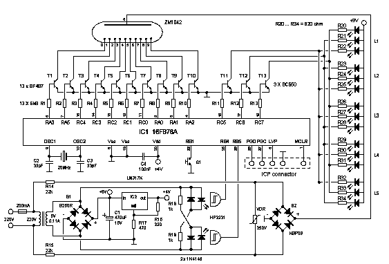
Figure 15 Complete circuit diagram of Geert's clock.
(Click on the diagram to download a detailed circuit diagram in pdf format)
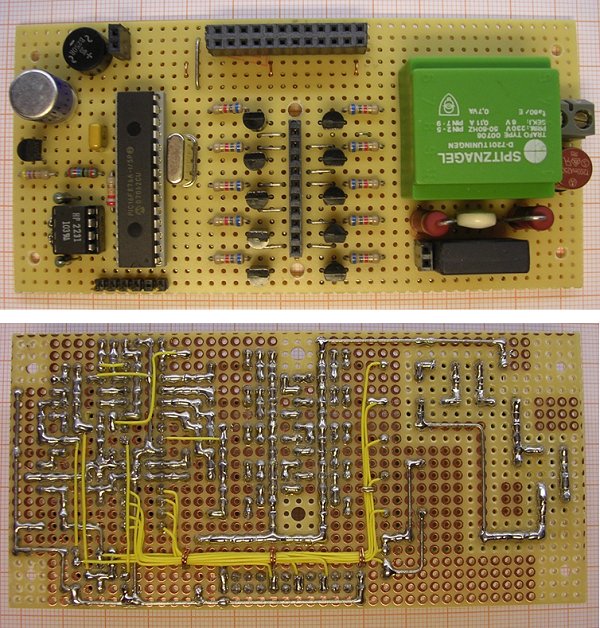
Figure 16 Front- and Backside of the main PCB.
Figure 16 gives an impression of the clock PCB. It should be stressed again that
all metal parts in this circuit carry a potentially lethal voltage with respect to
ground. Since the clock will only be used in a closed box this is not problem.
Special care was taken to isolate the screws used to fix the PCB in the box from the
mains. As can be seen in the photograph of the bottom side of the PCB the copper islands
around the screws and between other points carrying high voltages were removed.
This can be easily done by sticking the point of a welding iron in the hole.
A small twist and a pull removes the copper island (as least for these PCBs).
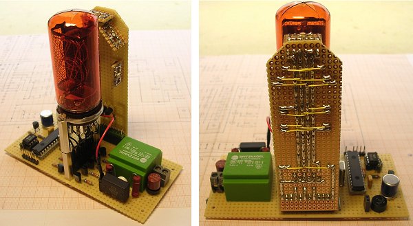
Figure 17 Different views of the complete clock.
Figure 17 finally shows the final circuit with the "LED tower" from front and backside.
Quite some force is needed to remove the tube from its socket. To avoid damage to
the tube I connected the tube to the PCB with a simple connecter. When I need to remove
the tube it can stay in the socket this way. Similarly the "LED tower" is mounted on the main
PCB with a simple connector.
After the discussion of the dimmer software on this page and the
description of the software for the
farewell present of Jan Verhoeven, the complete program for this clock will hold
little surprises. The program basically consists of a main program and an interrupt
service routine which is called every 100 µs. The main program takes care of the
displaying of the time in right order and is very simple. The interrupt service routine
calls a set of routines which take care of: software implementation of the flip-flop,
filtering of the mains frequency, time keeping, dimming of the NIXIE, implementation of the
ambient light feature, and finally debouncing of the push-button key. All-in-all an
impressive lists of tasks.
The NIXIE digits are turned on by routine "nix-on". The value in W on call of this routine
determines the digit to be turned on. The routine works with what is called a computed
goto: the value in W is multiplied by two and then added to the program counter. The next
instruction to be executed determines which digit is ignited. This routine is placed
in page 3 together with the color lookup table. The reason is that both perform a
manipulation with the program counter. When the lower eight bits of the program counter
are modified, the higher order bits are loaded from "PCLATH", by placing both routines in
the same page "PCLATH" only needs to be set once.
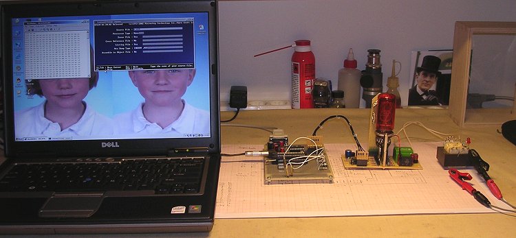
Figure 18 The set-up during software development. From left to right: Laptop, Wouter Ooijen's in circuit programmer [1], the clock and one of the back-to-back isolation transformers.
I discovered that the controller could not reliably be programmed at a Vdd of 4 Volt. So during
in system program development I temporarily disconnected the LM317 controller and used an
external 5 Volt power supply instead. This worked fine.
The pseudo-random color sequence that is displayed by the color LEDs is stored in
a separate include file. In the zip file that can be downloaded I have included three
different colour include files. Have a look at the page on
Jan Verhoevens farewell present for a more detailed
description of these files, and how they can be included.
The compressed file which can be downloaded here , contains the following files:
Rather poor quality movie but it gives an impression of the ambient light feature.
The time shown is 13:46

Father's day 2009.