If you are interested in Flyback Converters you might want to
keep track of my present project:
the µTracer:
a miniature radio-tube curve-tracer
Click here to read about my “low-noise” 6 to 90 V converter project which replaces the anode battery in battery tube receivers.
introduction
In the NIXIE clocks that I have built, I did not want to have the big and
ugly mains transformer in the actual clock itself. Instead I use an AC
adapter that fits into the mains wall plug. This means that I have to use
some sort of an up-converter to generate the 180V anode supply for the NIXIEs.
This page describes a simple boost converter and a more efficient flyback
converter both of which can be used as a high voltage power supply for a 6
NIXIE tube display. Frans Schoofs beautifully explained to me the working
of the flyback converter and much of what he explained to me you find
reflected on this page. I additionally explain the essentials of inductors
and transformers that you need to know. This is just a practical guide
to get you going, it is not a scientific treatise on the topic.
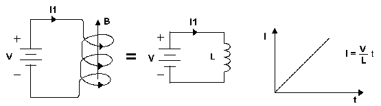
Consider the simple circuit consisting of a battery connected to an
inductor with inductance L and resistance R (Fig. 1).
When the battery is connected
to the inductor, the current does not immediately change from zero
to its maximum value V/R. The law of electromagnetic induction,
Faraday's law prevents this. What happens instead is the following.
As the current increases with time, the magnetic flux through this
loop proportional to this current increases. The increasing flux
induces an e.m.f. in the circuit that opposes the change in magnetic flux.
By Lenz's law, the induced electric field in the loop must therefore
be opposite to the direction of the current. As the magnitude of the
current increases, the rate of the increase lessens and hence the
induced e.m.f. decreases. This opposing e.m.f. results in a linear increase
in current at a rate I=(V/L)*t. The increase in current will finally
stop when it becomes limited through the series resistance of the
inductor. At that moment the amount of magnetic energy stored in the
inductor amounts to E=0.5*L*I*I.
Figure 1
In words: the inductor does not allow for any abrupt changes in the current.
When a change in applied voltage occurs, the inductor will always generate
an e.m.f. that counteracts this change. When the circuit is interrupted
for instance, the inductor will still try to maintain the current flowing
by generating a very high voltage over its terminals. Usually this will
result in a spark in which the magnetic energy stored in the inductor
is released. This particular behavior of inductors is used in boost converters
to boost the voltage to levels above the battery voltage.
Materials like ferrites can be used to increase the magnetic flux in an
inductor. When a magnetic field is applied to a ferrite the small magnetic
domains in the ferrite will align with this field and increase its magnitude.
In this way inductors can be made smaller and with lesser turns and thus with
smaller series resistances (smaller losses). Note that the flipping
of these domains costs some energy, but in good ferrites this can be very small.
With increasing magnetic flux more and more magnetic domains point into the
direction of the field. At a certain point all the magnetic domains point
into the direction of the field and at that point we say that the ferrite
saturates.
Any further increase in current will only result in a small
increase of flux, basically as if the ferrite was not present. Since
most ferrites have a very high permeability, already small currents
can result in a high magnetic flux. As a result the ferrite will
saturate at a current which is not practical for power conversion
applications
Ferrite cores for inductors and transformers for power applications
therefore have an air gap. An air gap reduces the effective
permeability and thus the magnetic flux. The larger the air gap, the stronger the
reduction in flux an the higher the maximum current the inductor can
handle. We say that the magnetic energy is stored in the air gap.
The photograph shows several inductors for DC/DC converters salvaged from old
PCBs from PCs, Laptops etc. If you consider playing with DC/DC converters
it is best to buy at least one decent inductor with a known inductance,
series resistance and maximum current. The inductor in front of the
picture is the 100uH "reference" inductor I use.
The boost converter is perhaps the simplest of all switched mode converters.
It uses a single inductor without the need for "difficult" transformers.
It's working can best be explained with the simplified circuit diagram
given in Fig. 2. Here the transistor is represented by an ideal switch
and the control circuitry has been omitted. The dissipation by the NIXIE
tubes is represented by the load resistor Rload. A high voltage capacitor
C is used to buffer the output voltage. In a typical configuration
the input voltage would be something like Vbat=12V and the output voltage
Vout=180V.
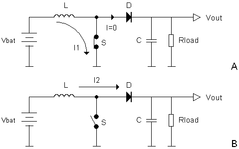
Figure 2 Simplified circuit diagram of a boost converter.
At t=0 the switch closes (Fig. 2A). As a result the current through
the inductor will start to increase linearly according to
I=(Vbat/L)*t. At a certain moment the switch is opened by the
control circuit (Fig. 2B). The current at that monent has reached
a certain value Ipeak. We have
seen in the previous section that the inductor wants to keep the
current flowing through it's windings constant, whatever it takes.
The switch is open, so the only way the inductor can achieve this
is to forward bias diode D so that the current (and thus the energy)
can be dumped in the buffer capacitor C. Now remember that the
capacitor was charged to 180V! So in order to forward bias the diode,
the inductor has to generate an e.m.f. (or induction voltage) of something
like 180-12=168V., something like a "controlled spark. The current now
quickly drops according to I=Ipeak-(Vout/L)*t. For Vbat=12V and Vout=180V
this means that it will take only a fifteenth (180/12) of the time it took
to reach Ipeak when the switch was closed, to drop again from Ipeak to 0
now the switch is open. After a certain time the whole process repeats
at a rate of f times per second.
So far so good. However, the boost converter has a serious disadvantage.
To understand this we first have to consider the switch that we have been
using. In a real circuit most likely a power MOS transistor will be used
as the switching element. In the boost converter this transistor will
have to handle both a high current when the switch is closed and a high blocking
voltage when the switch is open! For the transistor this is a difficult
combination. In order to make the transistor withstand high blocking voltages,
the manufacturer of the transistor has to include regions in the transistor
that will accommodate these voltages so that the intrinsic transistor
will not breakdown. However, when the switch is closed (transistor conducting),
these regions will result in additional parasitic series resistances
and thus in an increased Ron. This is the reason why transistors with a high
breakdown voltage always have a higher Ron than transistors with a lower breakdown
voltage. Since the currents can be quite high, this inevitably means
losses in the form of dissipation in the transistor. As we will see in one of the
next sections this problem is solved in the fly-back converter by the use of a
transformer.
By balancing the amount of power stored in the inductor to the amount of power
dissipated in the load it is possible the calculate the output voltage of the
boost converter.
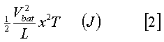
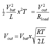
Every second the amount of power dissipated by the load is:
If T is the total cycle time, and x the fraction of T that the switch is closed,
then the maximum current in the inductor is:
The energy per package delivered by the inductor is:
In one second f=1/T packages are delivered so the amount of energy delivered
per second is:
Since in steady-state the amount of energy delivered should equal the amount
of energy used [1]=[2]:
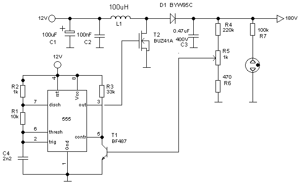
A simple boost converter high voltage supply for NIXIEs
If you want to build a simple DC/DC converter to lighten up your NIXIEs and you don't
care to much about the conversion efficiency, even if it means a (small) heatsink
for the power transistor, then the boost converter is the best choice.
But even if you think of building a real fly-back converter than it is a good idea to
start with a simple boost converter. The boost converter only requires an "of the shelf"
inductor and when you have it working it is easily converted into a fly-back converter
by a few small modifications.
Figure 3 Simple 12-180V boost converter using the 555 as controller.
The circuit is very simple and closely follows the circuit topology of Fig. 2. For the
transistor I have used a BUZ41A. This transistor is rated at a maximum Vds=500V and an
on resistance of 1.5ohm at 4.5A. Equivalent or better types like the IRF730 will also
perform well. The diode should be a fast switching type like the BYW95C or better.
An old (computer) power supply will yield you most of these components. The inductor
I picked from a catalogue and is 100µH with a few tenths of an ohm series resistance
capable of handling several Amps of current.
The most interesting aspect of the circuit is how an ordinary 555 is used to regulate
the output voltage. Now, there are hundreds of switched mode controllers ICs on the market
which are all better suited for this job than the 555. The problem with all these ICs is
that if you build a nice NIXIE clock using them, and at one moment in the future
the IC breaks down, it is more than likely that it is already obsolete and out of
production. The 555 is (very) cheap, performs well enough and most likely will remain
in production forever.
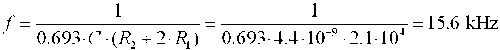
To understand how the controller works it is best to first understand how the 555 functions.
On the internet you may find a number of excellent 555 tutorials [1,2]. Without R3 and T1
the 555 is configured as a normal astable multivibrator running at a frequency of:
Without any feedback, the output voltage at this frequency will be well
in excess of 200V. However, the voltage divider formed by R4, R5 and R6
has been designed and adjusted in such a way that when the output voltage
reaches 180 V, T1 just starts to conduct. This is at a base-emitter voltage
of ca. 0.8V. Now remember that the 555 works by charging and discharging
the capacitor between 1/3Vcc and 2/3Vcc as defined by an internal
resistor ladder network. When T1 starts to conduct it will pull down
the internal supply voltage of this network resulting in a smaller
voltage swing and hence a higher frequency. From the last equation
in the previous section we learn that a higher frequency (smaller T)
will result in a lower output voltage. In this way the output voltage
will settle at a value determined by R5. For T1 I have used a high voltage
type. There is really no need for that and any small signal npn transistor
with a decent gain will work. A drawback of such a simple controller is that
the circuit has no protection at all against short circuits or overload situations.
An accidental short circuit of the output will therefore always result in a
defect power transistor (as I have experienced quite a number of times).
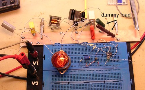
Figure 4 Testing the boost converter using a dummy load (and one NIXIE).
If you are in the testing phase, and do not want to connect the
power supply to the NIXIEs yet, it is best to connect a dummy load
to the output since the circuit is not designed to work without
a load. I always first find out what the current is that I want to
operate my NIXIEs on. I usually choose a value well below the operating
condition specified in the datasheet. This will greatly extend the
lifetime of the tubes. Using a high voltage supply I select the supply
voltage and the load resistor in such a way that with a minimum of current
the brightness of the tube is still good enough. Once the total current
and the voltage are known an equivalent load resistor can be calculated
from Rload=Vout/Itotal. During the testing phase this resistor
connected to the output replaces the NIXIE tubes.
A few words about safety. Although the 180 Volts are generated starting
with an innocent 12 Volt an accidental contact with the charged buffer
capacitor will be a painful, possibly a lethal experience. Always be
very careful ! I always place a small neon indicator lamp at the output
of the converter (even in the final clock) to clearly indicate that
a dangerous voltage is present at the output. Additionally during
testing I permanently have a 20kohm/V multi-meter connected to the output
so that I always know the output voltage. Finally, the advice of my father
who was from the radio tube area: always keep one hand in your pocket
when touching the circuit when it is switched on. In that way the current
can never pass your heart.
When you want to start experimenting with boost or fly-back converters it is
good idea to buy at least one inductor with known parameters that may act
as a kind of reference device for the inductors or transformers that you make
yourself. I use a 100µH inductor with about 0.2ohm series resistance
capable of handling several Amps of current. It is especially designed for SMP
applications. The circuit depicted in Fig. 5 allows you to compare "an unknown"
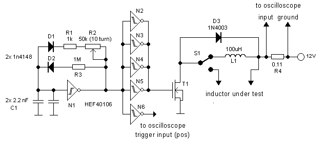
inductor (or transformer) with the reference inductor.
Figure 5 Circuit diagram of the inductor test bench.
The circuit is designed to test the inductor as closely as possible
under conditions that occur in the boost converter presented in the last
section or in the fly-back converter to be presented in one of the next
sections. Basically, the circuit is little more than the inductor which is
connected to the 12V power supply by transistor T1. The current through the
inductor is measured by the small series resistor R4. A voltage drop of
100mV over R4 corresponds to a current of approximately 1A. When the transistor
is opened, the inductor can dump its energy in diode D3. Since the voltage drop
over the diode is only 0.6V, it will take about 12/0.6=20 times as long for the
current to drop to zero (remember I=(V.t)/L). This is the reason why the
gate of the transistor is driven with a highly asymmetric signal generated
by the oscillator around N1-N6. The transistor on-time is determined by
C1 and R1+R2. R2 is set so that the transistor on-time is equal to the
transistor on-time in the converter under normal load. The transistor
off-time is determined by C1 and R3 and about a factor 20 longer than the
on-time.
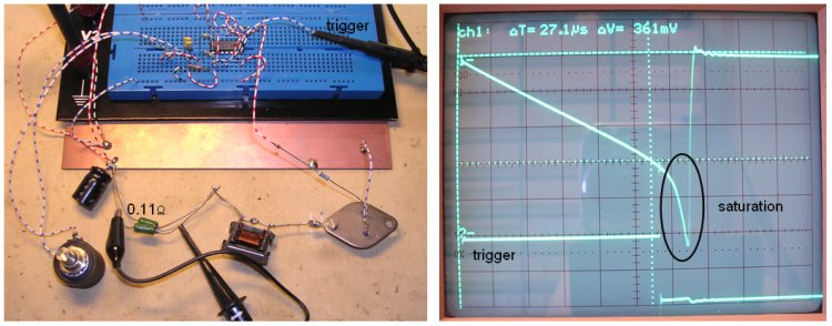
Figure 6 The inductor test bench circuit (left) and a measurement off the reference
inductor (right).
In Fig. 6 (right) you find a measurement of the reference inductor. We find that
with a supply voltage of 12V the current through the inductor reaches a value
of I=V/R=0.361/0.11=3.28A in 27.1µs. Since I=(V/L)t we find for the inductance
L=(V/I)t=(12/3.28)27.1=97.6µH. Not bad! At a little bit higher current we
observe a sharp increase in the current through the inductor. This is the point
where the ferrite saturates. The inductor should not be used beyond this point.
You may now want to try different inductors e.g. inductors salvaged from old
(computer) power supplies. Switch S1 make it easy to compare these inductors
with the reference inductor. Another important parameter to watch is the current
consumption of the test-bench. An increase in switching losses in the inductor
core is reflected by an increase in power consumption.
An alternative simple and quick way to measure the inductance of an unknown inductor can be found here.
This section deals with a few basic things you need to know about transformers
in order to understand fly-back converters. In Fig. 7 I have tried to sketch
an elementary inductor and its schematic equivalent. Note that both windings
have a certain direction and that equal directions are indicated by a dot.
Figure 7 Basic transformer with open secondary windings
In this example we assume that the primary side of the transformer has a certain number
of turns with inductance L1. The secondary side of the transformer has ten times that
number of turns. As a result the secondary side will have an inductance L2=10^2*L1=100*L1.
First consider the case that the secondary windings are not connected. When a voltage
source is connected to the primary coil the current through the primary winding will
start to increase linearly at a rate I=(V/L1)*t. Since with open terminals at the secondary
side no secondary current can flow, the transformer will behave as a normal inductor
with inductance L1. The increasing primary current will generate a magnetic flux not only
through the primary windings, but the same flux will also flow through the secondary
windings. It is easy to see from reasons of symmetry that if the secondary coil would
be identical to the primary coil the voltage at the primary and secondary side would be
equal. In this case we have 10 times the number of turns at the secondary side. This can be
seen as a series connection of 10 coils each carrying a voltage of 10V so that in total 100V
is induced at the primary side. The voltage of 100V at the output remains as long as the
current continues to increase linearly. In practice this means until the
current reaches its compliance or until the core saturates.
Figure 8 Basic transformer with closed secondary windings
Next the secondary winding is connected to some load which will allow for a current
to flow (Fig. 8). If the primary winding is now connected to some voltage source,
a current through the primary winding will start to flow, resulting in magnetic
flux in the direction as indicated by the arrow. This magnetic flux will
obviously also flow through the secondary winding. We have seen that an inductor
resists a change in magnetic flux. To counteract the increasing flux,
a current flowing in opposite direction through the secondary winding
will start to flow as indicated in Fig. 8
Resulting in a voltage drop over the load as indicated.
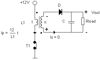
Figure 9 The transformer in flyback
Finally the voltage source at the primary side is suddenly removed (Fig. 9). The only way the
secondary winding can prevent a sudden collapse of flux is to reverse the direction
of the current flowing through the secondary winding. As a result alsothe
voltage drop over the load will reverse. Note that the voltage over the load
will increase to any value that is needed in order to maintain a constant flux.
The magnetic energy stored in the inductor is dumped into the load and the secondary current
decreases at a rate Vout/L2
Figure 10 depicts the basic elements from the flyback converter. Again all
control circuitry is omitted, and the switching MOSFET is represented
by an ideal switch.
Figure 10 Phase one, storing energy in the transformer.
For the moment we assume that at t=0 the buffer capacitor is charged to the
nominal output voltage Vout and that the current through the primary windings
of the transformer is zero. At t=0 the switch closes and a current will start
to flow through the primary winding. This will induce a voltage over the secondary
winding with a polarity as indicated (see previous section). Since the diode
is reverse biased no secondary current will flow, so basically the secondary
winding is "not connected". In other words at the primary side of the transformer
we "just see an inductor". As a result the primary current will start to increase
lineary according to I=(12/L1)*t.
During the time the switch is closed the voltage induced over the secondary
windings will be n*12V. This means that the diode minimally has to block a
reverse voltage of n*12+Vout
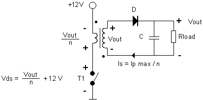
Figure 11 Phase two, dumping the energy from the transformer into the buffer capacitor.
At a certain moment the switch will open (Fig. 11). Lets call the current that was
flowing through the primary winding at the moment just before the switch was opened
Ipeak. The energy then stored at the moment of opening is 0.5*L1*(Ipeak*Ipeak).
The transformer wants to sustain the magnetic flux. Since the circuit at
primary side is open the only way the inductor can do this is by inducing a voltage
at the secondary side high enough (>Vout) to forward bias the diode. The initial value
of the current will be I2=Ipeak/n. During the time that the diode is forward
biased, the voltage over the secondary winding will equal Vout+0.8V. The 0.8V is the
voltage drop over the diode and can for a high output voltage like in a NIXIE converter be
neglected. The transformer will transform this voltage down to Vout/n. So the total
voltage that the switch has to block in open position is 12+(Vout/n).
Actually this is the big advantage of a flyback converter over a boost converter.
In a boost converter the switch (MOSFET) has to carry a large current during
the on phase and a high voltage during the off phase. In the flyback converter
the voltage during the off phase is transformed down to a value determined
by the ratio in turns. This means that a MOSFET with a much lower Ron can be used
(see section on the boostconverter).
Similarly, in the boost converter the diode has to carry both the high on current and
a high reverse voltage.
In the flyback converter the diode at the secondary side
only has to block a high voltage while the current is low (Ipeak/n). This makes it
possible to select a diode with smaller capacitances and hence higher switching
speed. All this results in reduced losses and an increased efficiency.
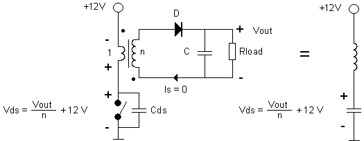
Figure 12 Phase three, energy dump completed discharge of drain-source capacitor
This continues until all energy stored in the transformer is dumped in the buffer capacitor.
At that moment I2 becomes zero (Fig. 12). At that moment the e.m.f induced at the primary
side (Vout/n) will vanish. However, the parasitic capacitance of the switch (source-drain
capacitance of the MOSFET) will be charged to (Vout/n)+12 V. At the primary side now a series
resonant tank is formed with a charged capacitor (Fig. 12 right). This will cause a dampened
oscillation.
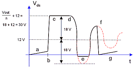
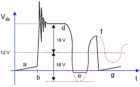
Figure 13 Voltage over the switch during all three phases
Figure 13 schematically shows the drain-source voltage (the voltage over the switch) during
all the phases of the converter just described.
During phase the switch is closed. What we see is the
voltage drop over the switch caused by the non-zero on resistance. During this phase the current
will increase linearly, so also the voltage drop over Ron will increase linearly. At point b the
switch opens. The secondary current will start to flow and the output voltage wil appear down
transformed over the primary winding. The total blocking voltage over the switch will
be 12+(Vout/n) (Fig 13c). At point d all the energy is dumped in the capacitor and the secondary
current drops to zero causing the induced e.m.f. at primary side to vanish. The charged
drain-source capacitor, now suddenly connected in series with the inductance of the primary winding
will result in a dampened oscillation (Fig. 12e). At point f the switch closes again, and any remaining
energy in the LC tank will be dissipated in the transistor.
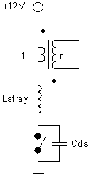
Figure 14 Stray inductance.
This leaves just one small phenomenon to be explained. No transformer is ideal. There will
always be magnetic field lines generated by the primary windings which are not (fully)
enclosed by the secondary windings. This will cause a stray inductance that can be modeled
as a small inductor in series with the primary winding of the transformer (Fig. 14). We have seen
that all the energy that is stored in the transformer is dumped in the buffer capacitor. This does
not hold for the (small) amount of energy stored in the stray inductance. So the sudden opening
of the switch will cause a sharp voltage peak, just as with any inductor which is suddenly
disconnected from a DC current. The small stray inductor in series with the source-drain capacitance
will cause a dampened high frequency oscillation (Fig. 15).
Figure 15 High frequency oscillations due to energy stored in the stray inductance.
If needed the switching transistor can be protected from the high voltage peak by an
RC snubber network or a zenerdiode which limits the maximum source-drain voltage.
Finally you can check for yourself the equation derived for the output voltage of
the boost converter also holds for the flyback converter. This is not really
surprising, like in the boost converter the flyback converter is based on the
dumping of the energy from an inductor or the primary winding of a tranformer
in the load. The transformer just serves to lower the voltage over the switch.
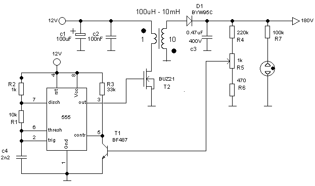
A flyback converter high voltage supply for NIXIEs.
After all what has been said so far, the circuit diagram of the flyback converter
will hold no surprises (Fig.16). Literally the only difference with the boost
converter is that the inductor is replaced by a transformer, and that the
transistor has been replaced for a BUZ21. The BUZ21 has a much lower on
resistance (Ron=0.085 ohm) as compared to the BUZ41A (Ron=1.5 ohm) but also
a lower drain-source breakdown voltage (100V versus 500V).
Figure 16 Circuit diagram of the Flyback converter.
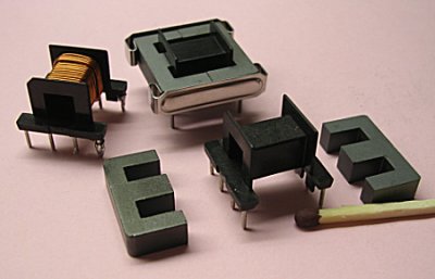
The difficult part of the circuit is the transformer. Well it is not
exactly difficult, but the problem is that you have to make it yourself.
What makes things worse is that finding a suitable ferrite core can some
times be difficult since component vendors often only have a few types
on stock. The E-shape ferrite core that I use measures 20x20x5 mm (Fig. 16)
I got them from Paul van de Broek who always helps me when I need
something special.
Figure 17 The ferrite core that I use (20x20x5 mm).
So what is the strategy for finding the number of turns you need on the
ferrite core that you have? Well first of all I always start with my inductor
test-bench so that I can compare what I have made with the reference 100 µH
inductor. If this is your first fly-back converter it might be illustrative to
first try the ferrite core without an airgap. Mind everybody always says airgap,
but what they actually mean is a spacer, often made from plastic (cellotape).
So start with say 10 or 20 windings without an airgap. What you probably will see
in the test-bench is a too high inductance (slower increase of current as
compared to the 100 µH inductor). At the same time you will find the
ferrite saturating at a low current. It is now time to include the
spacer. Attach a peace of cello tape and cut the excess amount of tape with a
razor blade so that only the touching surfaces of the ferrite are covered with tape.
If you try the inductor now you will find a much lower inductance and a higher
saturation current. Probably you will need to add or remove some turns to
get an inductance of 100 µH (same slope). For the primary winding I use
0.4 (or 0.5) mm diameter insulated copper wire. When you have determined the
proper number of primary turns, the secondary winding consists of ten times that
number of turns. For the secondary windings I use something like 0.1-0.15 mm diameter
wire. I always include a layer of tape in between two layers of secondary windings
to prevent arcing. The transformers that I use have 22 primary turns and 220 secondary
turns.
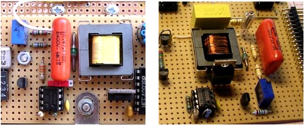
Figure 18 Two examples of the Flyback converter built on a peace of breadboard.
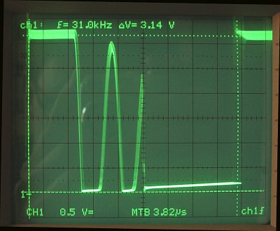
Figure 19 shows the drain-source voltage of power MOSFET measured with a 1:10
reduction probe. The 1- on the left axis marks the 0 V input level.
The image is not very sharp
due to some trigger jitter caused by a 50Hz ripple on the power supply. Nevertheless,
several features from Fig. 15 can be recognized. The repetition frequency is 32 kHz
and the maximum blocking voltage of the transistor is about 31 V according to theory.
The voltage over the transistor almost swings for two full periods until the transistor
switches on again. The high frequency oscillations due to the stray inductance are there,
but difficult to see on the photograph. The increasing voltage drop over Ron during
the on phase is clearly visible.
Figure 19 Drain-source voltage of power MOSFET measured with a 1:10
reduction probe.
The total converter can easily be built in an area of less than 4x4 cm. To increase the
lifetime of my tubes I usually run them on as low as current as possible. Typically
1-1.5 mA. This means that the converter has to generate for 6 digits about 6 to 7 watts.
The efficiency is ca. 80%. This is not spectacular but good enough for such a simple
circuit. If you decide to built one: have fun, be careful and good luck!


 Any further increase in current will only result in a small
increase of flux, basically as if the ferrite was not present. Since
most ferrites have a very high permeability, already small currents
can result in a high magnetic flux. As a result the ferrite will
saturate at a current which is not practical for power conversion
applications
Any further increase in current will only result in a small
increase of flux, basically as if the ferrite was not present. Since
most ferrites have a very high permeability, already small currents
can result in a high magnetic flux. As a result the ferrite will
saturate at a current which is not practical for power conversion
applications