If this is the first time you read about the uTracer, perhaps a little explanation is in order. About two years ago I had an idea to construct a tube tester / curve tracer. By using a pulsed measurement principle, the whole circuit could be kept very small. After several iterations, this led to the uTracer3. Many people liked the concept, and after many requests I decided to make a kit so that everybody could build their own DIY tube tester.
In the mean time some 60 uTracers are up and running in more than 20 countries and 4 continents! Although, without exception, people are very enthusiastic about their uTracer, there is always room for improvement. Both from people who have actually built the uTracer3 as well as from the thousands of people who have read the weblog, I received many emails with requests for improved / extended performance and added functionality.

Figure 1.1 A set of vintage beauties waiting for restoration left to right: Pilot T501 (done), NSF h207u, Philips LX452AB (battery tube radio), Philips BX200U (set for tropics).
On this page I want to make an inventory of these requests, and I want to test and compare circuit ideas to realize them. I have to emphasize here again that the goal is not to design the best all round, most complete tube tester that money can buy, but to find the balance between performance and complexity / costs! Having said that, I do not want to raise false expectations: I really have no idea if this will eventually result in a complete working system, let alone a commercial product! I write these pages primarily for my own documentation, and for communication with other enthusiasts. Making the uTracer3 kit has cost me a lot more time than I could have ever imagined, and besides making tube testers, there are many other projects waiting, such as the restoration of four beautiful vintage radios.
| to top of page | back to homepage |
Higher Anode and Screen voltages
This point is undoubtedly on top of the list of most people who have given me feedback. The maximum anode / screen voltage of 300 V is by many people regarded as the most severe limitation of the uTracer3.
So, why are the anode and screen voltages limited to 300V? At the beginning of this project I did some initial experiments, and I found that with standard available components the maximum output voltage of a straightforward boost converter is limited to approximately 450V. Since 100uF/ 400V electrolytic capacitors are commonly available and relatively cheap, I decided to limit the output voltage to 400V. And then again, during the experiments with the high voltage switches I decided to limit the output voltage to 300V because, given the simple circuit concept of the uTracer3, is was difficult to guarantee fully short-circuit proof outputs.
Personally I am not into Power Audio Amplifiers. For me the main motivation to build the uTracer was to have a means to visualize and study the phenomena which occur in more standard “small signal” tubes, so for me 300V was already more than enough. In the mean time I have learned that especially people developing and building power amplifiers are interested in triode characteristics up to much higher voltages. So the question is: how high? Values mentioned in emails I received vary from 400V, via 700V, all the way up to 1500V! I really could use some more input here: what tubes are commonly used in the somewhat bigger PA’s, and to what voltages and currents need they be characterized keeping in mind that there is always a trade-off between price and performance? Is there only a need for higher voltages for triodes, or are there also people who want to test pentodes to much higher voltages? Would a curve-tracer just for triodes be OK for most people? What type of tubes are you using? Any additional wishes ….
Extended grid bias range
More or less the same questions apply to the grid bias circuit. The grid bias voltage range of the uTracer3 is 0 to -50V. The choice for this range was on one hand given by practical reasons, such as supply voltage ranges of OpAmps and the maximum input voltage of the LM339 voltage regulator, and on the other hand by the fact that this range covers some popular tubes including the very popular EL34.
Figure 2.1 A PL509 tested at grid biases of -60 to -80 V with the aid of an external 50V voltage source.
Some creative solutions can be used to increase the grid bias range of the uTracer3. To be able to characterize a PL509 in the relevant bias range, Derk Reefman for example inserted an external 50V voltage source in series with the grid connection (Figure 2.1). I understand however that a somewhat higher (more negative) grid bias would be welcome.
Figure 2.2 The 801A is designed to be used for grid biases between -160 V up to 160 V.
I received one or two questions from people who would like to test tubes at positive grid biases. I have to admit that I had no idea that tubes were also sometimes used in this regime. As it turns out some tubes like the 801A, are even designed to be used at positive grid biases so that a higher output power can be achieved (More1,More2). The 801A is even specified for grid biases ranging from -160 V up to 160 V (Fig. 2.2)! A positive grid bias automatically results in a grid current which also needs to be measured.
Again, I am highly interested in the specifications that people “in the field” would like to see for the grid bias!
Larger heater bias range
To keep the uTracer cheap and simple an old laptop power cord is used as power supply. The idea is that most people have an old power cord lying around anyway, and if not they can by bought practically for free at flea markets, surplus shops etc. These power cords can easily deliver tens of Watts of power at an output voltage of approximately 19 V. With so much power available, it was natural to use some of it for the heater. By simply pulse-width-modulating the output of the power cord, heater voltages between 0 and 19V can be obtained with only a few transistors and an inductor. As it happens this covers quite a large range of tubes commonly used, but of course not all.
In the meantime it has become clear that the internal heater supply has difficulties with low voltages (< 4V) in combination with high currents (>1 A). It has become clear that this is a result of the PWM principle in combination with inductances in the heater circuit (More). This is certainly one of the things on my list to look into.
A number of people have asked me if it is possible to include a converter so that the uTracer can be extended to higher heater voltages. Personally I do not think it is worth the effort. Such a circuit will greatly increase the complexity, while it offers little additional functionality. Fortunately, the design of the uTracer3 is such that both for directly, as well as for indirectly heated tubes an external heater supply can be used. What I recommend as the most practical and economical solution is to use a simple external lab power supply for tubes with a heater voltage higher than 19V. For indirectly heated tubes, even a simple transformer can be used.
For low voltage / low current heaters, such as for delicate 1,5 V battery tubes (DL96, DK96, etc.), as well as for valuable vintage tubes, I personally always use a battery as heater supply. With a PWM regulator it is not so easy to accurately control the equivalent DC output voltage down to a tenth of a volt, especially not for low voltages. Additionally, in this way, under no circumstances, the heater can be damaged due to a hardware or software error. Next to these more rational arguments, I have to admit that emotionally I do not feel too comfortable to subjecting fragile heaters to a PWM signal with an amplitude of 19V! A few dry “A” cells can easily be included in the case and made accessible on the front panel.
USB Communications
A recurring “complaint,” especially on forums, is the lack of an USB interface. The good-old serial RS232 interface is considered to be outdated and obsolete. Well, what can I say? It certainly is a bit outdated, but by far not obsolete! There are still zillions of devices with a serial interface around interfaced to USB ports through cheap USB-to-serial converters. Even recent projects in leading magazines like Elektor are often RS232 based but use on board USB to serial converter. Basically there are a number of options:
Next to these “hot topics” there are some more minor issues which are on my personal wish list:
This list is by no means complete and will probably be expanded as this project develops. If you have suggestions, ideas, please mail them to me!
| to top of page | back to homepage |
Georg Beckman is one of the people who bought a uTracer3 from the first series. He actually wrote a very nice review about it on the RadioMuseum forum. He also wrote me a few emails with some very interesting circuit ideas. One of these ideas was to get rid of the “high-side” high-voltage switch altogether by using a transformer. He reasoned: “transformers can transform a low voltage pulse to a high voltage pulse. If we generate a low voltage pulse on the primary side of a transformer which is used backwards and transform it up to a high voltage, we can get rid of the high-voltage switch.” The principle of the idea is shown in Fig. 3.1. We have some “low-voltage” adjustable voltage source and a MOSFET switch which generates a pulse on the primary side of the transformer. On the secondary side of the transformer we then find a pulse with, depending on the turns ratio, a higher voltage which drives the anode or the screen. Since the secondary winding is floating with respect to the primary winding, current measurement can be simple done by adding a current sense resistor to the “cold side” of the secondary winding.
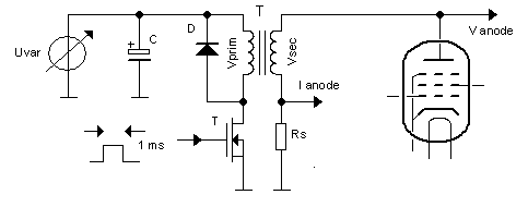
Figure 3.1 Principle of the transformer based high voltage bias circuit.
I have to admit that my first reaction was not very enthousiastic; one of the very nice features of the uTracer3 is that it doesn’t contain any heavy and difficult transformers, keeping the circuit small, cheap and light. Introducing a transformer seemed to me a step back in time. When we talk about low-loss switched-mode power supplies we always use low-loss ferrite based inductors and transformers. So (obviously) my first assumption was that Georg wanted to use some fancy, specially made, ferrite transformer. A quick “back-on-the-envelope” calculation showed that, given a measurement pulse length of about 1 ms, that would be almost impossible because of magnetic saturation of the ferrite.
The idea continued to intrigue me however. If it would work, it has some very nice features. The fact that the whole rather complex and “sensitive” high-side (PMOS/PNP) switch can be replaced by a normal robust low-side NMOS is obviously very attractive. Also current sensing by means of a small series resistor at the cold-side of the secondary side of the transformer is straightforward. On top of that the galvanic isolation between the high-voltage side and the low-voltage driving electronics seems attractive, although this argument might be more emotional rather than rational.
When I confronted Georg with my reservations he explained to me that it was not his intention to use a fancy ferrite transformer, but an ordinary, cheap, off-the-shelf mains transformer. I did some experiments on which I will report in subsequent sections, and became convinced that the idea might work. So assuming for the moment that the transformer idea works, how could a uTracer based on that look like?
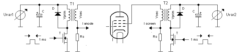
Figure 3.2 Two power supplies are needed to test tetrodes and pentodes.
First of all we need two of those transformer stages to bias both the anode and the screen grid independently (Fig. 2.1). Here already we run into a difficulty. One of the implications of using a transformer to generate high voltage bias pulses is that due to resistive losses in both the primary, but especially also the secondary (high-voltage) windings, as well as losses in the core, the voltage on the anode cannot be predicted accurately because it will depend on the current drawn by the tube! This doesn’t need to be a problem: although it cannot be predicted with great accuracy, it can be accurately measured! For a triode that is fine. Suppose we want to make an anode sweep, we then just make a best guess for the needed Uvar values (Fig. 3.1), but use the actually measured anode voltages for the plot. For a pentode or tetrode this is more difficult because here the anode sweep is made under the assumption that the screen bias is constant! Keeping the output voltage of the transformer bias circuit constant under varying load conditions is much more complicated and probably will require some iterative procedure. But nevertheless, let’s assume for the moment that we can fix that.
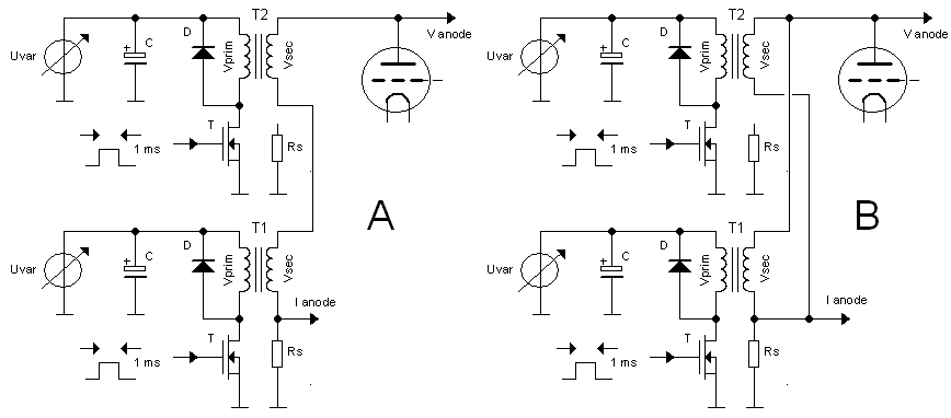
Figure 3.3 When a triode is tested the high-voltage supplies can be stacked or connected in parallel.
One of the very, interesting features of the concept is that the high voltage side is isolated from the driver side. This makes it possible to play some interesting tricks, provided that a triode is tested so that a separate screen supply is not needed. Occasionally I get questions from people who ask me for an option to test triodes to anode voltages in excess of 1000 V! By stacking two supplies (Fig. 3.3A) that is possible. Assume that each supply is capable of generating a pulse of 600 V at 200mA, then testing triodes to an anode voltage of 1200 V (@ 200 mA) becomes feasible. Alternatively, the two supplies might be connected in parallel to increase the output current to 400 mA (@ 600 V). These are indeed very nice specifications.
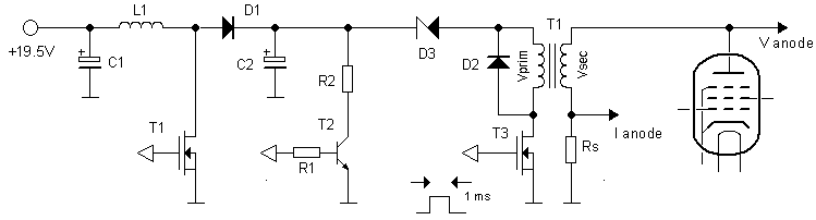
Figure 3.4 Idea for practical circuit implementation
Georg’s idea was to go directly from a low voltage to the required high voltage. What does that imply? Suppose that we use a power supply of 20 V and set the maximum high voltage at 600 V. This means a transformation ratio of 600/20 = 30 at least. In reality we will need a higher transformation ratio to make up for the losses. This means that the current at the primary side is at least a factor 30 higher than the current at the secondary side. So if we set – just as for the uTracer3 - the maximum anode current to 200 mA, this results in a primary current of at least 6 A, but more likely in excess of 10 A. Although that is not impossible, I am not really over-enthusiastic about the idea. I think it a better idea to use an intermediate high voltage of say something like 150 V and from there to use a transformer to step-up the voltage to 600 V. In that way the currents remain “manageable,” and since it requires less volume to store the same amount of energy at a higher voltage in a smaller capacitance (E=0.5*CV^2 with C inversely proportional, and V proportional to the volume) it also results in a (physically) smaller reservoir capacitance.
The actual circuit implementation I have in mind is something like the circuit shown Fig. 3.4. It consists of a small boost-converter identical to the one used in the uTracer3. The boost converter (L1,T1,D1) charges reservoir capacitor C2. If needed, C2 can be discharged through T2. Zener diode D3 removes the 19.5 V offset inherent to a boost converter. T3 pulses the transformer, while flyback diode D2 dissipates the energy that is released when T3 opens again.
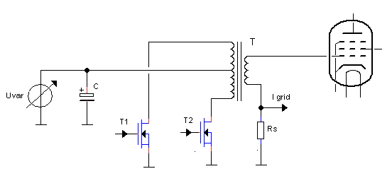
Figure 3.5 Generating negative and positive grid bias pulses.
Continuing along the same line of thought it may even be attractive to use a transformer in the grid bias circuit. In the uTracer3 a constant grid bias was used, generated by an OpAmp with a special “high-voltage” discrete output stage. There is actually no reason why the grid bias voltage should be a constant voltage. Just as the anode and screen supplies, also the grid bias circuit can be pulsed provided that the grid bias pulse precedes the anode and screen pulses to prevent unwanted anode current transients. By using a transformer with a center tap and an additional NMOS switch, it becomes possible to generate in a very simple and elegant way both negative as well as positive grid bias pulses (Fig. 3.5).
All this sounds very nice and attractive, however, the biggest problem as I see it right now is – as already discussed – the difficulty to predict the correct driver settings for a certain bias condition. The losses in the transformer combined with the fact that currents drawn by the tube are inherently unknown will require some kind of clever iterative scheme or mathematical procedure. Having uttered these words of caution, I cannot conclude else than that the whole idea seems attractive. Time for some experiments!
| to top of page | back to homepage |
Transformers can be tricky components to understand. Most people are more or less familiar with the operation of a transformer for AC sinusoidal signals, but when it comes to (DC) pulses, most of us feel a bit uncomfortable. To explain how a transformer behaves for pulses, we first have to build an equivalent circuit model of the transformer. Central component in such a model is a device which only exists in theory: an ideal transformer. Figure 4.1A gives the circuit symbol of an ideal transformer. The current voltage relations of this imaginary device are identical to the equations we know for the real transformers we are all familiar with, with this exception that these relations are valid for any waveform be it AC or DC.
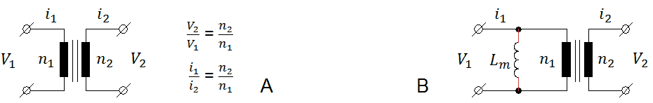
Figure 4.1 Left - ideal transformer, Right – the simplest model of a real transformer includes the magnetization inductance.
A real transformer (unfortunately) doesn’t behave like this. The reason is that we have used magnetic principles and effects to implement a practical version of this ideal device. Our everyday transformer is basically nothing more than two inductors which are magnetically coupled.
Figure 4.2 sketches what happens when a constant voltage is applied to the primary winding of a transformer with a turns ratio of n1:n2 = prim:sec = 1:2. The secondary winding of the transformer is left open in this example. The three rows of graphs in the figure show respectively the applied primary voltage, and the primary current and secondary voltage. The four columns show different moments in time. When the input voltage is first applied (Fig. 4.2A), the current through the primary winding increases linearly with time according I = V*t/L, with L the inductance of the primary winding. Since the magnetic flux (B) increases proportionally with the current (Ampere’s law), the voltage induced in the secondary winding (proportional to dB/dt, Lenz’s law) is constant. Since the ratio of the windings is two, the induced voltage at the secondary side will be twice the input voltage.
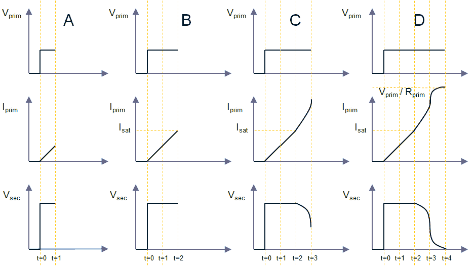
Figure 4.2 A constant voltage applied to a transformer with open secondary windings.
As long as the magnetic core of the transformer is not in saturation, the current will continue to increase linearly, and consequently the output voltage will remain constant (Fig. 4.2B). At a certain moment however, the core saturates. All the magnetic dipoles of the iron have now aligned with the magnetic field, and cannot help anymore to sustain a further increase in the magnetic field strength. In other words for a further increase in current, the transformer behaves as if the core was not there, resulting a sharp decrease in inductance and coupling between the windings. Due to the decreased inductance, the current through the primary winding will now show a sharp increase (Fig. 4.2C.) The output voltage of the secondary winding will collapse as a result of the vanishing coupling between the windings. Finally, the primary current is limited by the series resistance in the primary branch (Fig. 4.2D). When the current has become constant, the voltage at the secondary winding has become zero.
The simplest model of a real transformer is shown in Fig. 4.1B. In this model Lm represents the inductance of the primary winding with open secondary terminals. Lm is called the magnetizing inductance referred to the primary winding. The magnetization inductance models the magnetization of the core material. It is a real inductor showing saturation and hysteresis.
If we want to use a simple mains transformer as pulse transformer, what are then the boundary conditions for the input pulse (amplitude, duration) so that saturation is avoided? Iron cores saturate at a magnetic field strength B of around 2T (Bsat = 2T), but for off the shelf components the construction details needed to calculate the magnetic field are usually not available. Fortunately there is another method! We use the knowledge that mains transformers are designed to operate close to saturation under normal operating conditions. Knowing this, it can be shown (Appendix A) that the product of the pulse amplitude (V) and duration (t) should be V*t < 4.5 ms⋅Vrms (for 60 Hz transformers V*t < 3.8 ms⋅Vrms). For example, if we have a transformer with a primary winding of 36 V, then the V*t product of the input pulse should be less than 162 msV to avoid saturation. To take some extremes: a voltage pulse of 1 V during 162 ms, or a pulse of 162 V for only 1 ms.
Back to the idea of using a transformer to “boost” the high voltage pulses for anode and screen. The first choice is the transformation ratio. A high ratio results in high primary currents, while for a low ratio we could have saved ourselves the trouble of using a transformer. For the first experiments I picked a 10 VA transformer with two primary windings of 18 V (at nominal currents), which in series give 36 V, and a secondary winding of 220 V. Using a 6 V AC voltage I measured the transformation ratio of the secondary to primary windings which turned out to be 4.8. We have seen that for a 1 ms measurement pulse, the maximum amplitude of the input pulse for this transformer theoretically is 162 V, resulting in an unloaded output pulse of 4.8*162V = 780 V!
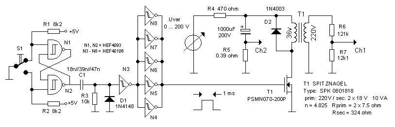
Figure 4.3 First test circuit used to test the pulse transformer principle
The circuit shown in Fig. 4.3 was used to test the new principle. Readers of my other tubes-tester weblogs will undoubtedly recognize my “standard” pulse generator circuit in the left part of the circuit diagram. The components have been chosen such that when S1 is pressed, the circuit produces a positive pulse of 1 ms. The energy for the primary high-voltage pulse is stored in a 1000 uF / 200 V electrolytic capacitor which is connected via a 0.39 ohm current sense resistor to ground. The capacitor is charged via R4 by a variable high-voltage power supply. R4 is selected such that during the pulse almost all the current through the transformer is supplied by the buffer capacitor. In that case the (negative) voltage drop over R5 is directly proportional to the current through the primary winding of the transformer. Flyback diode D2 absorbs the energy stored in the transformer when T1 switches off again. At the output I added a resistive voltage divider to reduce the output voltage to safe limits for my scope. The resistor values are a bit odd, but I happen to have these 1% resistors lying around. The division relation is
Vout = 11*Vscope.
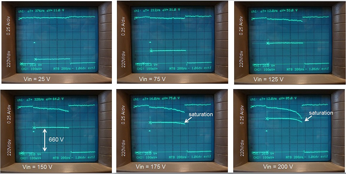
Figure 4.4 Primary current and output pulse for different input pulse amplitudes, and unloaded output.
Figure 4.4 shows in each photo both the current through the primary winding (top trace) as well as the output pulse (bottom trace). By the way, the current is measured over the sense resistor against ground, it appears as a negative signal. The output pulse amplitude increases linearly with the input pulse voltage (Fig. 4.6). For input voltages up to 150 V there are no signs of saturation. At that point the output pulse amplitude is 660 V! Note how the current almost linearly increases with time. At 175 V we observe, as expected, the onset of saturation near the end of the pulse. For 200 V the saturation becomes really pronounced, and we observe a sharp almost exponential increase in current.
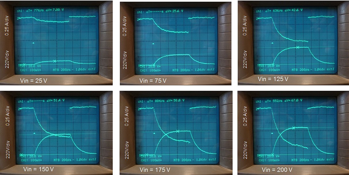
Figure 4.5 Primary current and output pulse for different input pulse amplitudes with a 3k3 resistor connected to the output of the transformer.
The next step is to test the circuit under load conditions. The simplest test was to redo the measurement above, but now with a 3k3 (10W) resistor connected to the output of the transformer. The output current will now be proportional to the output voltage. Just for reference, for an output voltage of 660 V the output current will be 200 mA, more or less my target output current value. We observe a number of striking differences.
First of all observe that the primary current is now much larger than in the unloaded case. A quick calculation: For an input pulse amplitude of 150 V, we find an output voltage of ca. 550 V. This results in a secondary current of 550V/3300Ω = 166 mA. This again results in a primary current of 4.82*166 mA = 800 mA, exacty the value we read from the photo.
We will consider the change in the slopes of the pulse and the absence of saturation in a next section, but first concentrate on the amplitude of the final pulse.
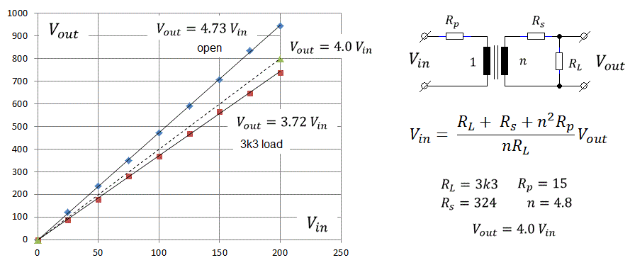
Figure 4.6 Output pulse amplitude versus input pulse amplitude taking losses into account.
In the graph in Fig. 4.6 the output voltage amplitude of the transformer has been plotted as a function of the input pulse amplitude for the case that the output of the transformer is left open and for the case that a 3k3 resistor is connected to the output (solid lines). For the loaded transformer the output voltages are obviously lower due to losses in the transformer. The circuit diagram in Fig. 4.6 shows the equivalent circuit of the transformer as far as DC resistive losses are concerned. The relation gives the output voltage of the transformer as a function of input voltage taking resistive losses into account. The dashed line in the graph gives the predicted input-output relation based in this relation and the measured DC resistances of the primary and secondary windings. We observe that most, but not all of the losses can be explained from the DC resistances of the transformer windings. Other losses can be caused by: discharging of the reservoir capacitor, series resistance of the capacitor, the current sense resistor and other losses in the transformer core and windings.
| to top of page | back to homepage |
When a load is applied to the output of the transformer, the shape of the pulse changes from a nice rectangular shape to a pulse with pronounced leading- and trailing edges (Fig. 4.5). This effect is caused by the leakage inductances of the transformer. These leakage inductances are associated with magnetic field lines originating from the primary winding which are not coupled into the secondary winding and vice versa. In the transformer model they are represented by two separate inductances in series with the terminal leads (Fig. 5.1A). In Fig. 5.1A also the series resistances of both windings have been included. For our purpose we will rewrite the transformer model of Fig. 5.1A into a slightly different model where the secondary leakage inductance and resistance have been referred back to, and included into, the primary leakage inductance and resistance (Fig. 5.1B). As long as Ls is much smaller than Lm, the transformer ratio of the ideal transformer hardly changes so it can still be approximated by n. By the way, a very simple method to measure Ls, is to short circuit the secondary winding and then measure the inductance at the primary winding. Short circuiting the secondary winding will short circuit Lm, leaving only Ls (Appendix C).
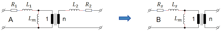
Figure 5.1 Complete model of a transformer including series resistances and leakage inductances.
If we neglect the magnetization current for a moment (which is a valid assumption under significant loads, compare Fig. 4.4 and 4.5), then all the output current has to pass Ls. The leakage inductance in combination with the output resistance forms an L-R combination with time constant τ = L/R. If we estimate from one of the graphs in Fig. 4.5 the time it takes for the current to increase to 63% (1/e) of its final value, we find ca. 200 us, this in combination with the output resistance of 3k3 gives a leakage inductance of L = τ*R = 200us*170Ω = 34 mH, which is for such a simple estimation close enough to the measured value of 22 mH (Fig. 5.2).
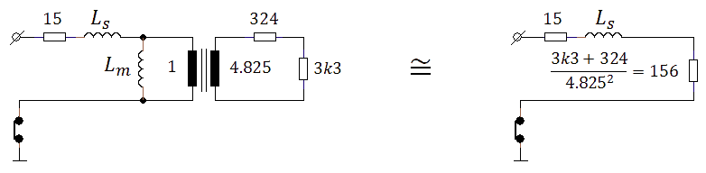
Figure 5.2 Estimation of the leakage inductance from the leading slope of the output pulse.
Note, that although in the measurements of Fig. 4.5 input voltages of up to 200 V were used, so well in excess of the “theoretical” saturation value of 162 V (for a 1 ms pulse), no saturation is observed! The reason is that it is the integral of the voltage over time (the area of the pulse) which counts, and which has to be less than the aforementioned 162 msV. So although it takes more time for the pulse to reach its plateau value, we can compensate for that by increasing the pulse length. The output pulse can be described by a simple first-order system resulting in an exponential behavior (Fig. 5.3). The time constant of this system is determined by the leakage inductance and the total series resistance referred to the primary winding. As long as the integral of the pulse over time is less or equal than the saturation criterion, no saturation will occur.
The leakage inductance results in a significant complication of the whole transformer pulse idea! With increasing load, the slope of the trailing edge of the output pulse decreases. As a consequence the length of the measurement pulse will have to depend on the load. On the one hand the pulse length has to be chosen such that the final plateau value (say to a value of 4τ, corresponding to 98% of the final value) is reached, while on the other hand it should not be chosen too long because otherwise the criterion for non-saturation is violated.
Figure 5.3 The output pulse shows a first-order exponential behavior.
When the MOSFET switch opens again, the current through the leakage inductance wants to remain constant. To achieve this, a voltage across Ls will develop so that the primary current continues to flow through the snubber diode. Gradually, the energy stored in the inductor will be dissipated in the load resistor, and the current will drop, resulting in a trailing edge of the pulse with the same time constant as the leading edge. Note, that when the diode is extended with a zener diode, Ls will have to develop a higher voltage to maintain the same current. The higher voltage will result in a faster “discharging” of Ls (t=V*t/L) and hence a reduced fall time. This at the expense of a significant dissipation in the zener diode and a higher breakdown voltage of the MOSFET.
The measurement of Fig. 4.5 with a constant load resistor connected to the output of the transformer obviously results in an output current which is proportional to the output voltage. A pentode and tetrode however have output characteristics which much more resemble a constant current sink. In this case the pulse circuit has to be able to deliver high currents at low voltages. To investigate how the pulse circuit behaves under true constant output current conditions, a slightly different measurement was performed whereby the circuit was evaluated for a number of different output voltages rather than input voltages. So for each output voltage set point, a load resistor was connected which resulted in a current of either 100 mA or 200 mA, after which the input voltage was adjusted so that the desired output voltage was obtained.
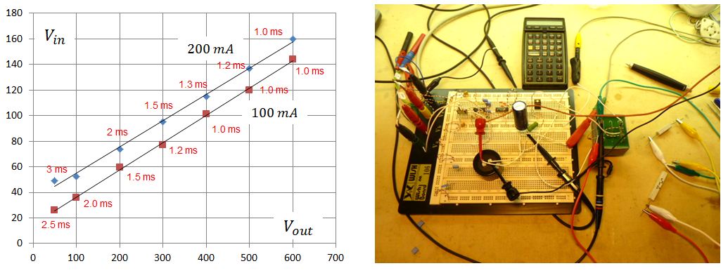
Figure 5.4 Input voltage required to reach a certain output voltage for a current of 100 mA or 200 mA.
Figure 5.4 shows the result of this measurement. Next to each measurement point the pulse length required to reach the plateau value is noted. The good news is that with a simple 10 VA transformer pulses up to 600 V at currents of 200 mA can easily be obtained. The bad news is that both the input pulse amplitude, as well as the optimal pulse length are a function of the load (current) which is not known beforehand. A measurement even will therefore inevitably involve some kind of iterative procedure to obtain the optimal settings.
What seem most challenging are high current pulses at low output voltages. In this case the load impedance is lowest, resulting in a large LR-time constant. The question is whether a plateau value can be reached, while still avoiding saturation. Figure 5.5 shows a measurement where the output voltage was set to 50 volts while the load resistance was decreased resulting in an increase of load current. So for every new measurement with a lower load resistance, the amplitude of the input pulse (noted in Fig. 5.5) was adjusted so that a 50 V output pulse was obtained. Remarkably, the output current could be increased to 500 mA without any sign of saturation. At an output current of 600 mA the onset of saturation can be observed. At that point the input pulse amplitude is 108 V!
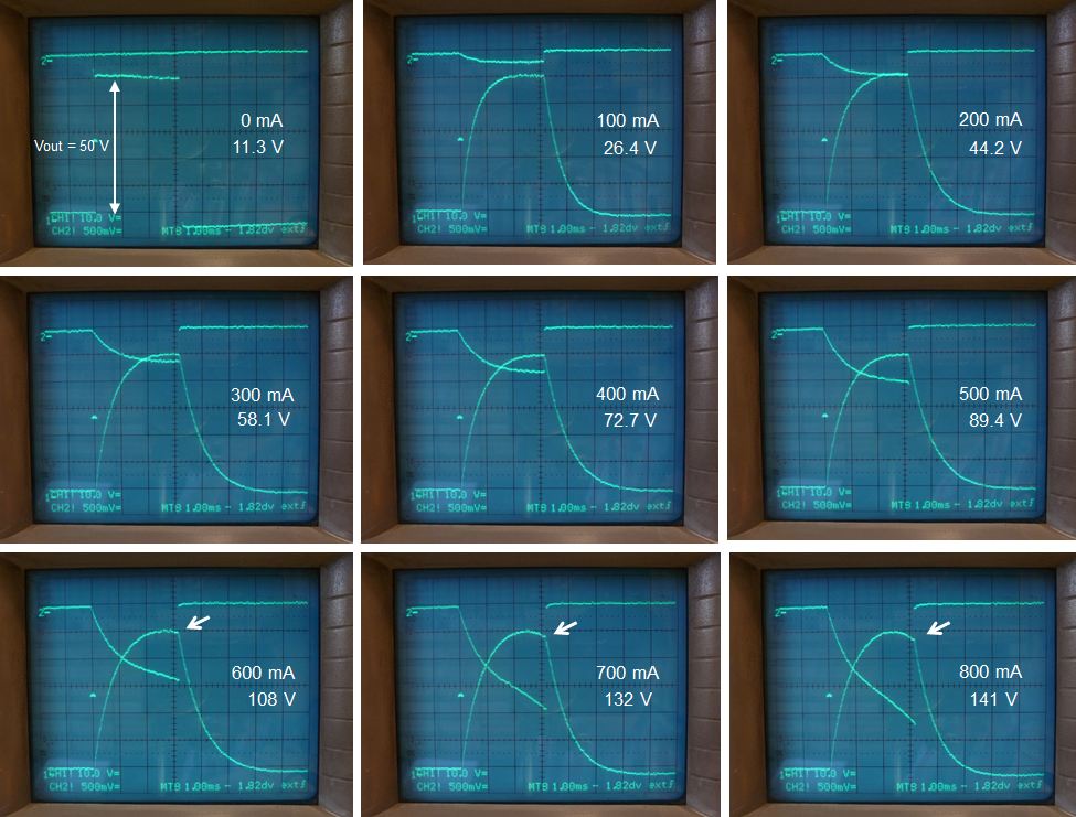
Figure 5.5 “worse case” test with a low output voltage and high output current (low output impedance situation). The output voltage was kept constant at 50 V while the load resistance was decreased.
| to top of page | back to homepage |
Lets try to summarize what we learned so far. A simple mains transformer can be used to “boost” a voltage pulse. When the transformer is unloaded, the output pulse will be rectangular, and the “boost factor” will be almost equal to the ratio of number of turns secondary/primary. To avoid saturation, the area of the input pulse (amplitude times duration) should be smaller than a certain non-saturation criterion which depends on the design of the transformer. When the output of the transformer is loaded, two effects complicate the situation. In the first place the amplitude of the output pulse will drop due to resistive losses in both the primary, as well as the secondary windings. In principle this is not so bad because we can compensate for that by just increasing the amplitude of the input pulse. The other effect is that the leading edge of the output pulse changes from a rectangular shape into more gradual “first order” increase characterized by a time constant τ. This time constant is proportional to the leakage inductance of the transformer, and inversely proportional to the load resistance. As a result higher load currents require a longer measurement pulse duration than smaller load currents. At the same time care has to be taken not to violate the non-saturation criterion. Fortunately nature helps a bit here: the higher the load current, the longer the pulse, but also the more gradual the increase in voltage, and since it is the integral of voltage versus time that counts, the integral also increases at a slower pace. For high load resistances on the other hand the measurement pulse cannot be too short, because we need some time for the electronics to stabilize and for the AD conversions themselves. In short, both the amplitude as well as the duration of the measurement pulse are variables which depend on the actual load being measured, which is in principle unknown!
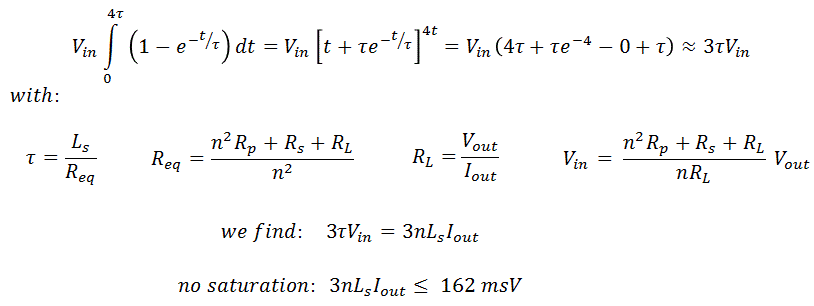
Figure 6.1 Saturation criterion calculation for a pulse length of 4*τ.
In this section I want to have a look at how the optimum duration of the measurement pulse has to be chosen in relation to the output current and voltage. As mentioned, the output pulse behaves like a first order system characterized by a time constant τ (Fig. 5.3). In order for the pulse to stabilize to a certain constant plateau value, I decided that the pulse length should be at least 4 times τ. In that case the voltage has stabilized to within 2% of its final value. In order to avoid saturation, the integral of the voltage over time from 0 to 4*τ has to be less than the saturation criterion (162 msV for our test transformer). Figure 6.1 shows the calculation of this integral, and quite remarkably we find that this integral only depends on the output current, and not on the output voltage. As long as the 3*n*Ls*Iout is less than 162 msV, saturation is avoided.
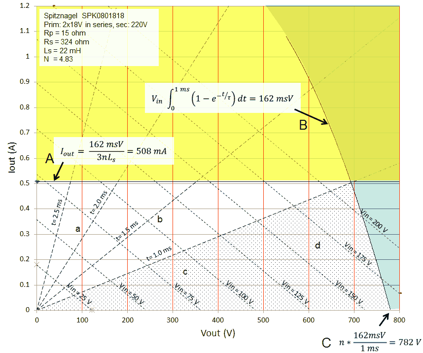
Figure 6.2 Vout / Iout selection plane and boundaries.
Figure 6.2 shows in a (rather complicated) graph the complete output voltage (x-axis) and output current (y-axis) space. In the area below line A, the integral of the voltage over time from 0 to 4*τ is less than the saturation criterion of 162 msV. So the conclusion is that as long as we can scale the duration of the measurement pulse with the time constant τ inversely proportional to Req (see Fig. 6.1), saturation will only occur above a certain current level, regardless of the output voltage. However, the higher the output voltage, the shorter the measurement pulse. Unfortunately, the measurement pulse cannot be made too short. Some time is needed for the electronics to stabilize and also the AD conversions take some time. So let’s say the minimum measurement pulse length is, just as in the uTracer3, 1 ms. How does that then limit the possible output voltage/current values?
Figure 6.3 Saturation criterion calculation for a fixed pulse length of 1 ms.
To find that limit we have to calculate for which Vout/Iout pairs the area of the input pulse for a fixed length of 1 ms equals the saturation criterion (Fig. 6.3). Unfortunately the resulting equation cannot be solved analytically (at least I couln’t), but the numerical solution is shown in Fig. 6.3 by line B. So for a constant pulse length the area right to line B is forbidden. The total operation range is now reduced to the uncolored area below line A but left to line B. The highest output voltage that can be obtained is with an unloaded output, indicated by point C.
Figure 6.4 Calculation of lines with constant pulse length.
The dashed lines in Fig. 6.2 indicate the measurement pulse length corresponding to 4*τ. The calculation of these lines is straightforward and given in Fig.6.4. In the shaded area below the line for 1 ms the pulse length corresponding to 4*τ is less than 1 ms. So in this area a constant pulse length of 1 ms is used as explained above. As a result this area is on the right side limited by line B. Above the 1 ms line the optimal pulse length has to be increased as indicated. Finally, the dotted lines in Fig. 6.2 give the required amplitude of the input pulse for a certain Vout / Iout combination, based on a simple model only including resistive losses.
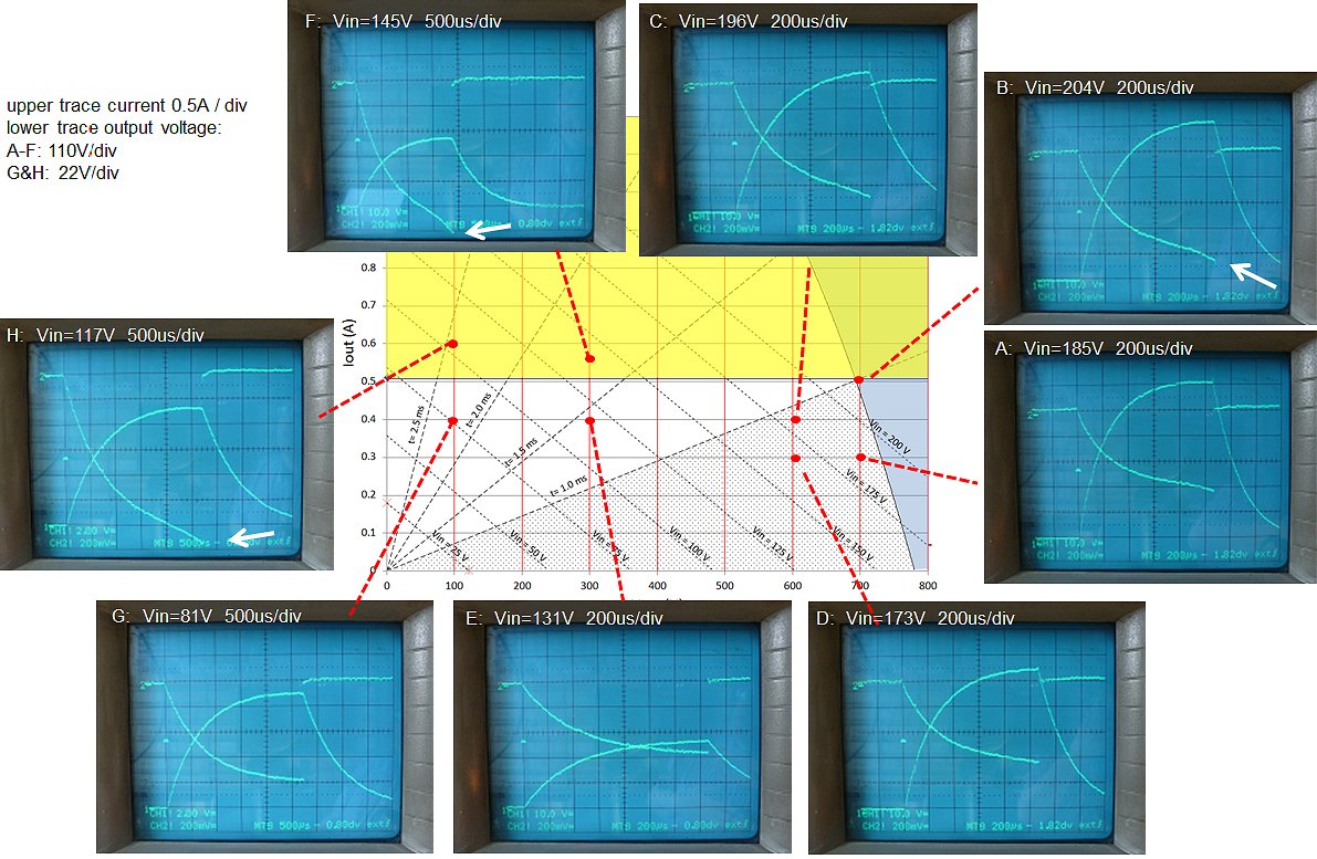
Figure 6.5 Checking the validity of the model.
In Fig. 6.5 the validity of the theory is explored along the boundary of the valid measurement region. For each measurement first a target output voltage was selected and a load resistor was connected which would result in the desired output current. Next the amplitude of the input pulse was increased so that the target output voltage was obtained. The standard time base was 200 us/div, for some measurements the time base had to be increased. In general I would say that there is a very reasonable agreement between the experiments and the simplified model. For all the points in the “forbidden” area, saturation is observed (white arrows), while the points within the white area are saturation free. Also the predicted input amplitude and measurement pulse length are in fairly good agreement.
| to top of page | back to homepage |
The experiments and calculations in the previous sections tend to convince me that the whole “transformer idea” actually might work! But so far we only considered the generation of the pulse itself. However, during the pulse a considerable amount of magnetic energy is built up in both the core of the transformer as well as in the leakage inductances, and as soon as the pulse is over, that energy has to go somewhere! The question more precise is: how can we de-magnetize the transformer in an efficient way, and quickly enough so that it is completely de-magnetized before the next measurement pulse. Because if the core is not completely de-magnetized before the next pulse, the field of the new pulse will add-up to the field already in the core, eventually resulting in magnetic saturation.
What happens after the MOSFET switch opens again at the end of the pulse is far from straightforward, and in a subtle way depends on the measurement conditions, especially the load. In this section we will first look at the situation when there is no load, or when the load is very small (low current). We will then consider the case when a substantial load is connected to the transformer.
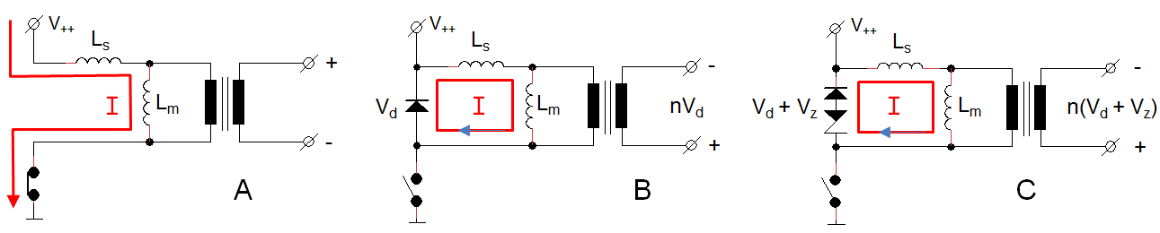
Figure 7.1 Current distribution during and after the measurement pulse in case the transformer is not loaded.
Figure 7.1 shows the current distribution in the transformer during and after the measurement pulse in case the transformer is unloaded. Figure 7.1A depicts the current distribution near the end of the measurement pulse. The MOSFET switch is still closed, and since there is no current through the secondary winding, the only current through the primary winding is the magnetization current through Lm. Since Lm is large, this current is relatively small, in our case something like 100 mA. When the MOSFET switch is opened, the currents through Ls and Lm initially remain constant. To achieve this, the voltage across Lm has to change polarity so that the snubber diode starts to conduct. The voltage drop across the diode is very small, in the order of 1 V. This voltage appears transformed at the secondary side of the transformer, resulting in a voltage of approximately -5 V for this particular transformer. The low voltage drop over the diode also has a disadvantage: remember that the current through an inductor as a result of a constant applied voltage is I = (V*t)/L. In other words the time it takes to (de-)magnetize an inductor to a certain current is: t = (I*L)/V. So when V is small, e.g. 1 V in the case of a simple diode, it takes approximately (0.1*2.3)/1 = 230 ms before the current through Lm has dropped from 100 mA to zero. This is way too long if a number of measurement pulses needs to be fired in quick succession. To reduce de-magnetization time, a zener diode is connected in series with the diode. To maintain a constant current the moment the switch is opened, Lm now has to develop at least the zener breakdown voltage across the transformer terminals. When a sufficiently high zener voltage is chosen, it is possible to de-magnetize the transformer in a few milliseconds.
Figure 7.2 Output voltage at the secondary side of the transformer for the unloaded transformer. The amplitude of the input pulse was 150 V. Column A represents the case only a diode snubber was used. For columns B-C a zener/diode snubber was used with a zener breakdown voltage as indicated.
The pulsing of an unloaded transformer is illustrated by the measurements in Fig. 7.2 which, by the way, were not without difficulties. In all measurements the output voltage of the transformer was recorded with a memory scope. In column A only a single snubber diode was used. In columns B,C and D, a diode/zener combination was used with zener breakdown voltages of 24 V (B), 72 V (C), and 172 V (D). The upper row of photos shows a global picture of the output pulse shape. In the lower row of photographs, both the vertical, as well as the horizontal axis have been magnified to highlight especially the negative voltages occurring after the measurement pulse. For the lower row of pictures, the measurement pulse itself is not clearly visible, but the beginning of the pulse (the trigger moment) is indicated by the small white triangle, while the 0 V line is indicated by the ”1-“ marker.
At first sight, a single snubber diode (Fig. 7.2 A1) results in the cleanest pulse. However, on magnification (Fig. 7.2 B1) we observe a long negative de-magnetization tail with a duration of at least 120 ms. If new measurement pulses were to be issued during this tail, the currents would accumulate, eventually resulting in saturation. The addition of a zener diode clearly results in a negative output pulse (Fig. 7.2 A1,A2,A3). With increasing zener voltage, the amplitude of this negative pulse increases, but the length of the pulse decreases proportionally! For a zener voltage of 172 V, the de-magnetization time has reduced to less than 10 ms (Fig. 7.2 B4).
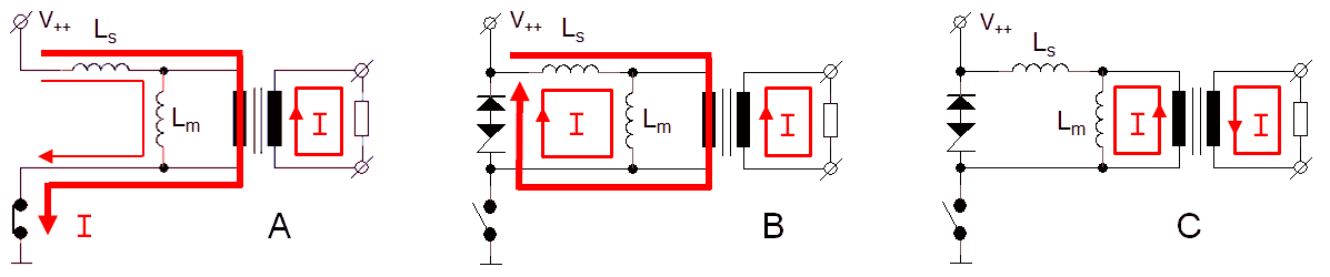
Figure 7.3 Current distribution during and after the measurement pulse in case the transformer is loaded.
The situation changes significantly when the transformer is loaded. Figure 7.3 shows the current distribution in the transformer circuit near the end of the measurement pulse in case a load is connected to the transformer. Next to the current through the magnetization inductance Lm, there is now an additional current caused by the load. Under significant load conditions, this current will be much larger than the magnetization current. If we assume e.g. a transformation ratio of 1:5, and a load of 300 mA, then the current caused by the load will amount to 1.5 A. So, despite the fact that Ls is usually much smaller than Lm, also a significant amount of energy is now stored in the leakage inductance. In fact, under realistic load conditions the amount of energy stored in the core is about equal in magnitude to the amount of energy stored in the leakage inductance. When the MOSFET switch is opened (Fig. 7.3B), the large current through Ls will continue to flow. To achieve this, Ls will develop such a high voltage that the zener/diode combination will open. Since the current through Lm initially also cannot change, the current through Ls remains flowing through the load. A lot of energy is now dissipated in the zener diode, resulting in a linear decrease in current. At a certain point, the current through Ls has become zero. However, since the inductance of Lm is much larger than the inductance of Ls, it will take a much longer time for the magnetization current to drop to zero. After the load current through Ls has become zero, the current still running through Lm can follow two paths: through the zener/diode combination or through the load. The current through Ls had no choice, it had to go through the zener snubber. The magnetization current however, will follow “the easiest” path and rather than developing a high voltage to open the zener, it will (slowly) discharge through the load. Note that to do that the current through the load will change sign!
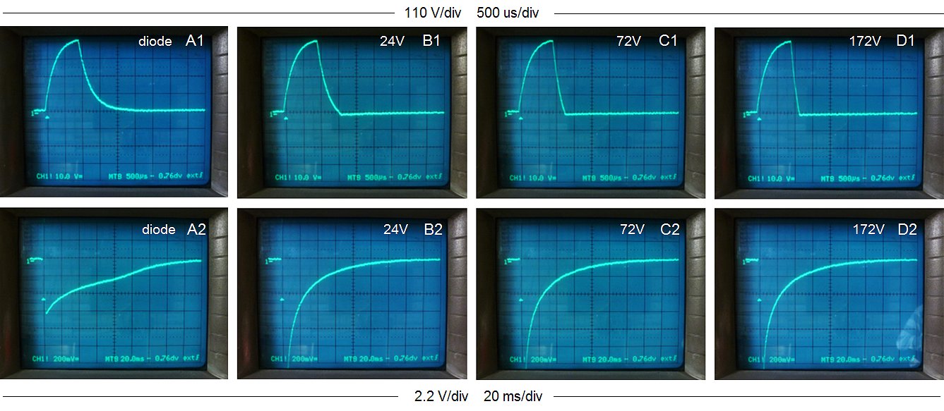
Figure 7.4 Output voltage at the secondary side of the transformer when the output is loaded with a 1.5 kΩ resistor. The amplitude of the input pulse was 150 V. Column A represents the case only a diode snubber was used. For columns B-C a zener/diode snubber was used with a zener breakdown voltage as indicated.
The whole process is illustrated by a series of measurements shown in Fig. 7.4. Again the output voltage of the transformer is recorder with the memory scope, but this time a load resistor of 1.5 kΩ was connected to the output. Just as for the previous measurement in column A only a single snubber diode was used. In columns B,C and D a diode/zener combination was used with zener voltages of 24 V (B), 72 V (C), and 172 V (D). The upper row of photos shows a global picture of what is happening. In the lower row of photographs both the vertical as well as the horizontal axis have been magnified to highlight especially the negative voltages occurring after the measurement pulse. For the lower row of pictures, the measurement pulse itself is not visible, but the beginning of the pulse (the trigger moment) is indicated by the small white triangle, while the 0 V line is indicated by the ”1-“ marker.
When only a single snubber diode is used, Ls can basically only discharge through the load resistance. This will result in a logarithmic decay of the current with exactly the same time constant as the rising edge of the current (see also section 5). When a zener/diode combination is used as a snubber, the voltage across the zener diode will quickly de-magnetize Ls at a rate t = (I*L)/V. The higher the zener diode breakdown voltage, the faster Ls is de-magnetized. As soon as Ls has been de-magnetized, the current flowing through Lm remains. The decay of this current is shown in the lower row of photos in Fig. 7.4. Note the enormous difference in both voltage as well as time scale between the series of measurements. Since Lm only has to develop a tiny voltage to maintain the current, the de-magnetization progresses logarithmically at a very slow pace, of course independent of the zener breakdown voltage. The complete de-magnetization of the core takes at least 160 ms! Fortunately, there is a beautiful trick to speed things up a bit.
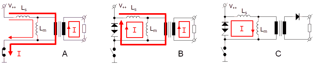
Figure 7.5 Current distribution during and after the measurement pulse in case the transformer is loaded and a blocking diode in the circuit at the secondary side of the transformer is used.
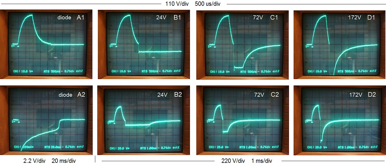
Figure 7.6 Output voltage at the secondary side of the transformer when the output is loaded with a 1.5 kΩ resistor and a blocking diode in circuit at the secondary side of the transformer is used. The amplitude of the input pulse was 150 V. Column A represents the case only a diode snubber was used. For columns B-C a zener/diode snubber was used with a zener breakdown voltage as indicated.
The process is again illustrated by four measurements Fig.7.6 A1-D1. In all four measurements the diode in the secondary circuit was used. The difference between the A,B,C,D measurements was, as in the previous examples, the breakdown voltage of the snubber zener diode. When only a simple diode snubber is used, the de-magnetization of the core proceeds almost the same as in the case when no diode is used in the secondary circuit. However, when a zener/diode combination is used as snubber, the de-magnetization of the core proceeds very quickly. The higher the zener breakdown voltage, the faster the de-magnetization occurs. Note that the area of the negative part of the output voltage pulse is always the same, regardless of the zener breakdown voltage. For a zener diode breakdown voltage of 172 V the core de-magnetizes in only 5 ms.
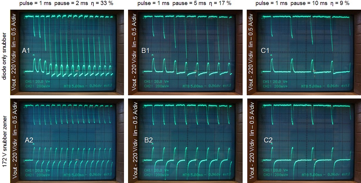
Figure 7.7 The transformers response to a quick succession of measurement pulses. In the upper row a single snubber diode was used across the primary winding while in the lower rom a zener/diode (172V) combination was used. The transformer was loaded with a 1k5 resistor. The input pulse amplitude was 100 V.
Whereas this all may sound very nice, “the proof of the pudding” as the English say, is a test whereby the transformer is subjected to a quick succession of measurement pulses with a minimum delay in between. For this experiment the test circuit of Fig. 4.3 was modified so that the push-button was replaced by a pulse generator. The resulting output pulses and input current was recorded with the memory scope. The circuit was connected to a load of 1k5 and the amplitude of the input pulse was 100 V. The pulse width was fixed at 1 ms, while the pause between two pulses was 2, 5 or 10 ms.
The upper row of three photos shows the input current and the output voltage of the test circuit with only a snubber diode across the primary winding. Observe that for every pulse the amplitude of the current increases. Apparently even a pause of 10 ms is not enough to demagnetize the transformer. At a certain point the amplitude of the current pulses seams to decrease. This is due to the fact that the high-voltage reservoir capacitor (1000 uF, 200V in this case) slowly discharges. Also note that the base line of the voltage at the secondary side drops below zero. With the zener/diode snubber (lower row of photos) the current pulses and output voltage pulses are constant indicating that the transformer is completely de-magnetized, even for a pause of 2 ms!
“That infernal zero!” was what Peter Blanken - a colleague of mine and a transformer expert with whom I’ve had many discussions during the writing of these pages - remarked when he saw the measurements. In the upper row of measurements the base-line of the output voltage drops below zero so that the average output voltage remains zero. In the lower row the negative pulses compensate for the positive pulses. Alas, I again failed to invent the DC transformer!

|
The photo impression to the right has absolutely nothing to do with tube-testers. It is just a personal souvenir to a very nice – though rainy - long-weekend to Vielsalm, the Arden in Belgium in May 2013 where these sections were written. |
| to top of page | back to homepage |
The first time I heard of the term “ruggedness” in the context of electronic circuits was in the mid nighties. At that time I was working at Philips Research on a project aimed at the development of a new generation of RF-power transistors for mobile phones (GSM). Just for the insiders, these were: double-poly silicon transistors, with an implanted base and poly-emitter, a selective collector implant and an Ft of 30 GHz. The most important design parameters for these transistors were the gain and the output power. Another, vaguer design constraint was the “ruggedness.” The transistors had to survive a total miss-match at the output (broken off, or shorted antenna) at the maximum supply voltage (phone connected to charger). This requirement really was a pain in the neck because, as so often in nature, there was a trade of between the gain and the requirements for ruggedness. Now, almost 20 years later, I am confronted with the same problem for the uTracer.
One of the design constraints of the uTracers is that they have to be short circuit proof at maximum output voltage to protect the circuit against operator faults and flash-overs. It was this design constraint which actually made me limit the output voltage of the uTracer3 to 300 V.
In this section the “ruggedness” of the transformer pulse generator concept will be investigated.
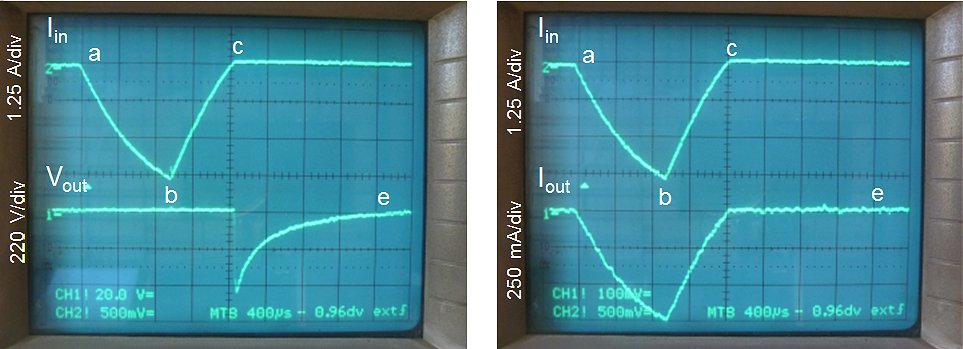
Figure 8.1 Pulsing the circuit with output short circuited @ Vin = 200V.
The first measurement that was performed was to pulse the transformer with shorted output at the maximum input pulse amplitude of 200 V, and a pulse duration of 1 ms. No protection circuit whatsoever was used. The left photo of Fig. 8.1 shows the current in the primary winding (upper trace), and the output voltage (lower trace). The right photo in Fig. 8.1 again shows the current in the primary winding on the upper trace, together with the current through the secondary winding on the lower trace. The peak input current is almost 4 A. The output voltage remains zero until the leakage inductance is de-magnetized, and then becomes negative during the de-magnetization of the core since the de-magnetization diode was used in the series with the load in the secondary circuit. The output current reaches a maximum peak value of 750 mA. This doesn’t seem much, but it represents a peak dissipation in the secondary winding of P = I^2*R = 324*(0.75)^2 = 182 W! The circuit servived the repeated short circuit test easily without the slightest problem.
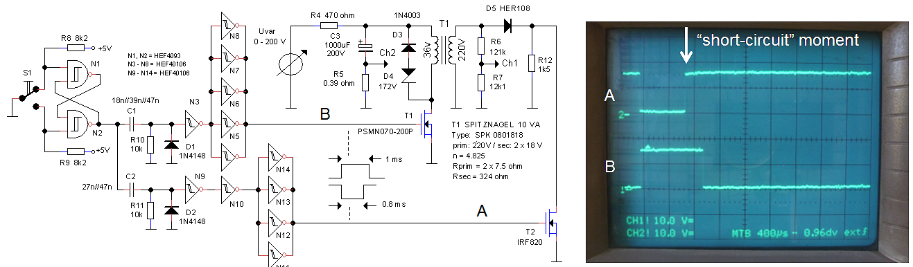
Figure 8.2 Test circuit used to simulate flash-overs.
In reality a short circuit can also occur as a flash-over in the tube during operation. To test the ruggedness of the circuit against flash-overs the test circuit of Fig. 8.2 was used. The circuit contains an additional high voltage transistor T2 which short circuits the output of the transformer at approximately 800 us after the start of the high voltage pulse. The simulated flash-overs are shown in Fig. 8.3. In both cases the input pulse amplitude was adjusted so that T2 just would not go into avalanche. Figure 8.3A shows the flash-over simulation with unloaded output. The input pulse amplitude in this case was 100 V. The upper trace shows the current through the primary winding, while the lower trace shows the output voltage. Point “a” marks the beginning of the high voltage pulse. Since there is no load connected to the output, there is only a small current flowing as a result of the magnetization current through Lm which increases linearly with time (“b”). At point “c” the simulated flash-over occurs, and T2 closes forcing the output voltage to zero. This causes a sharp increase in current as the current starts to built-up in the leakage inductance Ls. At point “d” the high voltage pulse is over, and the core and leakage inductances de-magnetize quickly as a result of the zener/diode snubber.
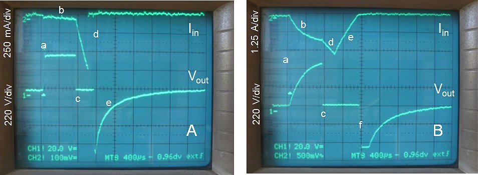
Figure 8.3 Simulated flash-overs. A) under no-load condition @ Vin = 100V , B) under nominal load condition Rload = 1k5 @ 180 V.
Figure 8.3B shows the flash-over simulation in case the output is loaded with a 1k5 resistor, corresponding to a maximum output current of approximately 330 mA. Point “a” again marks the beginning of the high voltage pulse. With the load connected, there is a large current flowing which increases logarithmically due to the leakage inductance Ls (“b”). The output voltage also increases logarithmically until at point “c” T2 closes, resulting in a sharp increase in input current (“d”). At the end of the measurement pulse Ls demagnetizes through the zener/diode combination resulting in a linear decrease of the input current (“e”). After Ls has been fully de-magnetized, the core also demagnetizes through the zener/diode snubber resulting in a negative output pulse (“f”).
In reality the effect of a short circuit is even less serious since the output current is continuously monitored, similar to the over-current protection in the uTracer3. As soon as the output current exceeds a certain maximum value, an interrupt is generated which terminates the measurement pulse within micro-seconds. The fact that a transformer represents a huge inductance thus appears to be extremely beneficial to make the circuit short-circuit proof. Due to these inductances the currents in the transformer change at such a slow pace that, on the time scale of the measurement pulse, they cannot reach dangerous values, let alone when the active over-current protection circuit is used. This intrinsic robustness of the transformer pulse generator circuit is really a huge advantage!
In Summary
At this point it seems a good moment to make up the balance and come to a first tentative circuit for the anode/screen pulsed power supply. First a list of pro’s and con’s:
The pulsed high voltage supply circuit as I have it in mind at this moment is the simplicity itself. On the left we find the software controlled boost converter which is nearly identical to the boost converter for the uTracer3 with the exception of D2 which has been added to allow output voltages down to 0 V. The projected maximum output voltage is 200 V. D3-D5 take care for a quick de-magnetization of the transformer. The output current is measured as a voltage drop over current sense resistor R7. Since this voltage drop is negative it is inverted by OpAmp IC1. The actual output voltage is measured

Nice! An advertisement found on “marktplaats” (the Dutch version of eBay) offering 2 EL34 tubes with test report, taken with the uTracer!
| to top of page | back to homepage |
Sometimes one takes things too easily for granted. It has always been such a given factor to me that the output voltage of a boost converter can never be lower than the input voltage that I never questioned it. It was one of the reasons why in the version 3 uTracer the cathode of the tube is references to the positive supply voltage rather than to ground. For the transformer based circuit I was planning to solve it by inserting a zener diode with a voltage larger than the supply voltage in series with the output of the boost converter (see section 2). This solution has the obvious disadvantage that there is a kind of “dead region” in the output voltage range of the boost converter which has to be compensated for my means of some kind of calibration. Furthermore the voltage drop over the zener diode will not be constant, and vary a bit, especially for voltages just above the zener voltage.
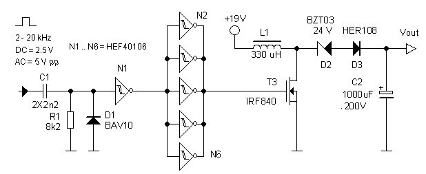
Figure 9.1 Breadboard circuit used to test the “rail-to-rail” boost converter concept.
It occurred to me that a much better solution is to shift the zener diode one position to the left so that it makes part of the boost converter (Fig. 9.1). The breakdown voltage of the zener diode is chosen such that it is higher than the supply voltage. What happens is the following: when the boost converter is off, the zener diode is not conducting and the output voltage is zero. When the boost converter starts working the flyback pulses of the inductor will increase to such a voltage that the zener diode starts conducting, and a current will flow into the reservoir capacitor. Obviously the zener diode takes away some of the reserve of the boost converter since it dissipates some energy. Figure 9.1 shows the test circuit used to test the idea. In this example a very large reservoir capacitor of 1000uF / 200V was used. The input circuit produces pulses of 30 us. Without the zener diode it takes the boost converter seconds to charge the 1000 uF capacitor to 200 V. With the zener diode included this increases to 7 seconds. Both a BZT03C24 as well as the better available 1N5934BG work equally well. The 1000 uF is perhaps a bit of an overkill. In the final circuit perhaps a 470 uF capacitor will suffice. In that case the charging time will be halved.
”Rail-to-Rail” OpAmp?
One of the improvements that I have in mind with respect to the uTracer3 is to get rid of the negative power supply. In the uTracer3 the negative power supply is used for three things: the negative grid-bias circuit, the low-pass filter OpAmp which makes a DC signal out of the PWM generator for the grid bias, and the inverting OpAmps in the current sense circuits. I will deal with the first two later and concentrate now on the inverting OpAmps.
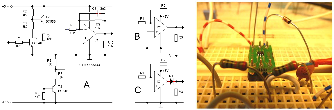
Figure 9.2 Breadboard circuit used to test the “rail-to-rail” OpAmp.
One of the drawbacks of having an enormous stock of components is that these components always tend to be “a bit out of date.” Obviously when a circuit is finally working, there is not a real motivation to go searching for modern alternatives. For the uTracer3 this happily coincided with my plan to use as little SMD components as possible, because most modern components are no longer available in “through hole” packages. The OPA333 is such a component. It is really a beautiful OpAmp with specification which a few years ago would have been unheard of. It is designed for rail-to-rail operation at a maximum power supply voltage of 5 V and an offset voltage of only 10 uV! The latter specification is only possible by using a special auto-calibration technique which zero’s the offset of the OpAmp every 8 us. The only drawback of the raltive small bandwidth (350 kHz) and slewrate (0.16 V/us) which is “on the edge” for this application.
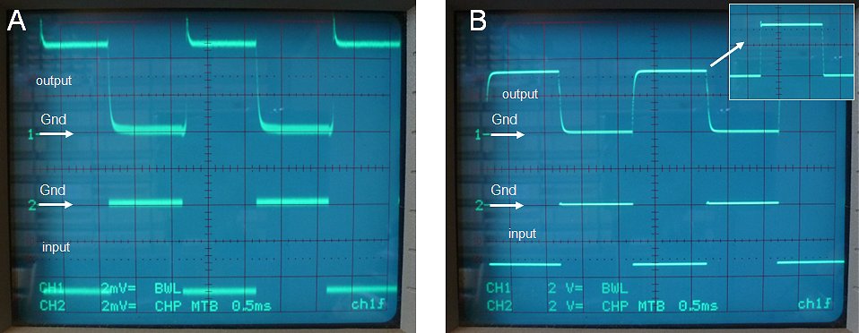
Figure 9.3 Behavior of the inverter circuit for small and large amplitude pulses.
“Rail-to-rail” however appears to be a relative notion. From the datasheet we learn that the specification for the minimum output voltage is approximately 15-30 mV above the lower supply voltage, ground (for a load resistor of 10k). Unfortunately 15 mV is quite a lot. If e.g. like in the uTracer3 we use a sense resistor of 18 ohm, then 15 mV corresponds to 0.0015/18 = 83 uA. The datasheet of the OPA333 explains that by connecting the output of the OPA333 to a negative voltage via a 40k resistor, also ground, and even slightly negative voltages can be obtained (Fig. 9.2B). A negative voltage was however something I was trying to avoid! A solution I had in mind myself was to include a (Schottky) diode in series with the output. The voltage drop over the diode would make it possible to include ground (Fig. 9.2C). A disadvantage is however that the output of the circuit would need a resistive pull-down. As it turned out, the diode circuit didn’t work out at all. I still do not exactly understand why, but with zero input voltage, the output voltage got stuck at about 270 uV?
It turned out that a simple pull down resistor of 10k to ground resulted in an output voltage of only several uV (Fig. 9.2A). To test the OpAmp in a circuit which approaches the real circuit as much as possible, the test circuit of Fig. 9.2A was built. The input of the circuit is connected to a 5V square wave signal source set to 500Hz. The pulse is transferred to T3 which pulses voltage R6/R7 down to -15V. By selecting the proper ratio for R6/R7 negative voltage pulse of any desired amplitude can be obtained. Fig. 9.3A shows both the input of the inverting OpAmp (taken at node R6/R7) and the output for an input pulse of only a few millivolts. The output tracks the input very well. Also for large signal with an amplitude of several volts, the circuit behaves very well. The slow rise and fall times at the output are for the largest part caused by the integrating capacitor C1. When C1 is removed the slopes become much steeper (inset), but the limited slew-rate of the OpAmp can be clearly observed.
”Dynamic on-resistance of the MOSFET switch” OpAmp?
With the transformer test circuit of Fig. 4.3 in place, I took the opportunity to check the on-resistance of the MOSFET switch at the primary side of the transformer. The on-resistance is not particular critical, but obviously it should not be too high, and after my experience with the dodgy IRF840 transistors in the uTracer3 I just wanted make sure I wasn’t overlooking something here. In the transformer experiments so far I used a PSMN070-200P. This transistor has a breakdown voltage of 200 V, which is a bit too low if we want to use the diode/zener snubber. In that case a higher breakdown voltage of at least 400 V is required.
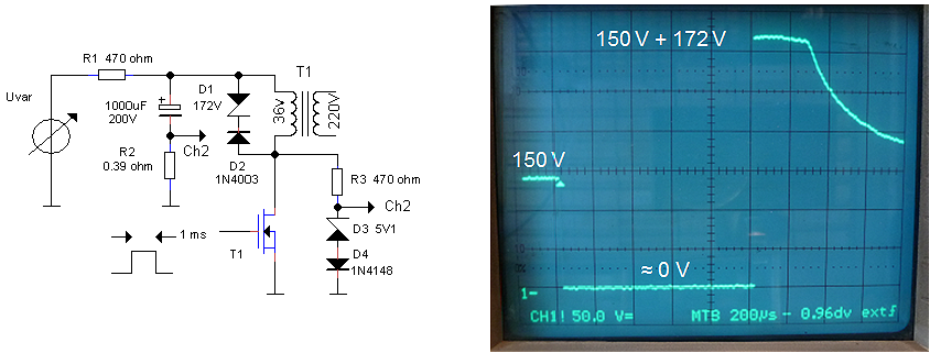
Figure 9.4 Determination of the dynamic on-resistance of the MOSFET switch.
Figure 9.4 shows a detail of the pulse test circuit. It allows for the simultaneous measurement of the current through the MOSFET - which appears as a negative voltage pulse over sense resistor R2 - and the voltage drop over the MOSFET. The ratio of the two gives the dynamic on-resistance during switching. To avoid overload artifacts of the scope, a simple clamp circuit consisting of R3, D3, and D4 was used.
The scope trace in Fig. 9.4 shows the voltage at the drain of the MOSFET with respect to ground. Before the pulse, the drain voltage is approximately 150 V, the supply voltage in this case. During the pulse the voltage drops to (nearly) zero. After the pulse the transformer de-magnetizes by developing a reverse polarity over its primary turn which opens the 172 V snubber zener diode, resulting in a drain voltage in excess of 300 V.
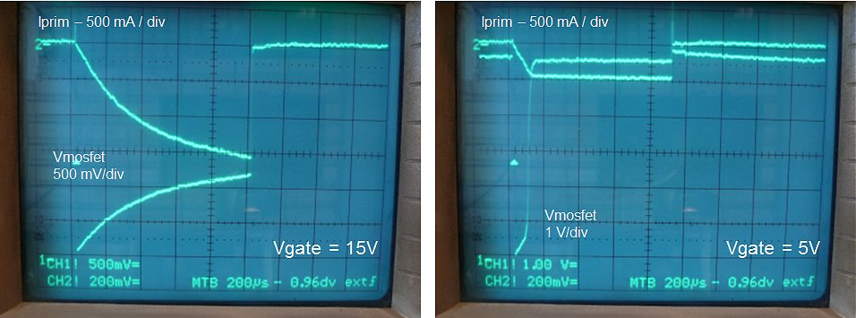
Figure 9.5 Voltage drop over a “doggy” IRF840 at a gate pulse amplitude of 15 V (left) and 5 V (right).
Figure 9.5 shows the same measurement, but in this case the vertical scale has been magnified to 0.5 V/div (lower trace) while the voltage drop over the current sense resistor has been added (upper trace). In the example of Fig. 9.5 one of the “doggy” IRF840 transistors was used. In the left photo a gate voltage amplitude of 15 V was used, while in the right photo a gate voltage pulse amplitude of 5 V was used. Proper operation at 5 V is important because I want to use a single power supply for the next generation tube testers. At a gate pulse of 15 V the transistor works fine with an on-resistance of approximately 1 Ω, which is comparable to the on-resistance of “good” IRF840 or a 07N60C3. However, at a gate voltage of 5 V we see that the current through the transistors saturates at 0.5 A, and that the voltage over the switch explodes, whereas for a 07N60C3 the on-resistance at 5 V is only marginally higher than at 15 V (not shown).
To wrap up, a simple and cheap 07N60C3 has an on-resistance of slightly less than 1 Ω at a gate pulse amplitude of 5 V under a maximum load condition of 1.5 A. The high breakdown voltage of 650 V allows for fast de-magnetization of the core.
| to top of page | back to homepage |
The first module that was built was the CPU module. I designed it into a stand-alone board so that it could be used in different configurations and experiments. The heart is again the 16F874 processor. All 40 pins of the processor can be probed via a female connector adjacent to the pins of the processor. There are three monitor LEDs La,Lb,Lc with amplifying transistors which can be used to monitor the level of any of the 40 pins of the processor.
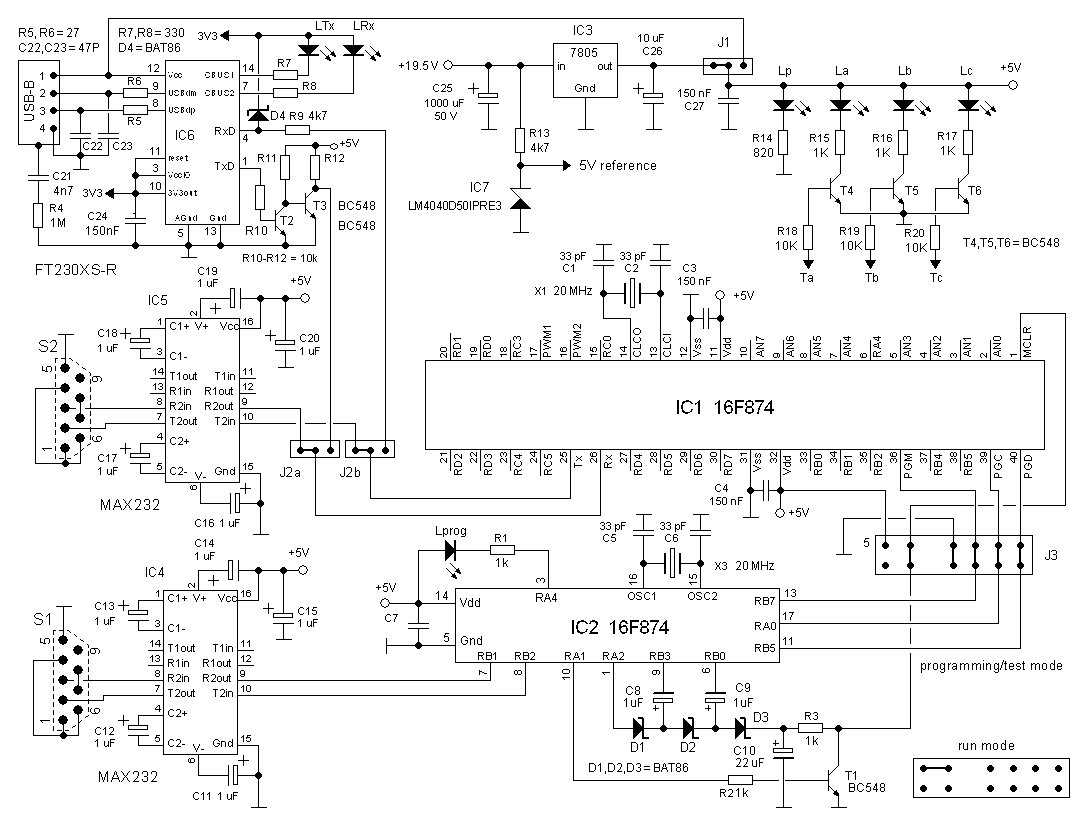
Figure 10.1. Circuit diagram of the CPU board
For the serial interface a standard MAX232 is used. I had never used one of the USB-to-serial chips from FTDI myself, so this board was a good opportunity to experiment with it. I used an FT230XS-R (Mouser: 895-FT230XS-R) from FTD in a tiny SSOP package. The chip is made in 3V3 CMOS. It has however 5V tolerant IO’s for the USB port and can be powered directly from the 5V USB port. In this mode it generates its own 3V3, power supply. Unfortunately the IO’s towards the processor are also 3V3 so that level shifters are needed to interface it with the PIC processor. I used a simple diode clipper consisting of D4, R9 to clip the 5V Tx signal of the PIC to 3V3. Two discrete transistors T2, T3 are used to bring the output level of the FT230 to standard TTL levels. This arrangement appears to work perfectly for my purpose.
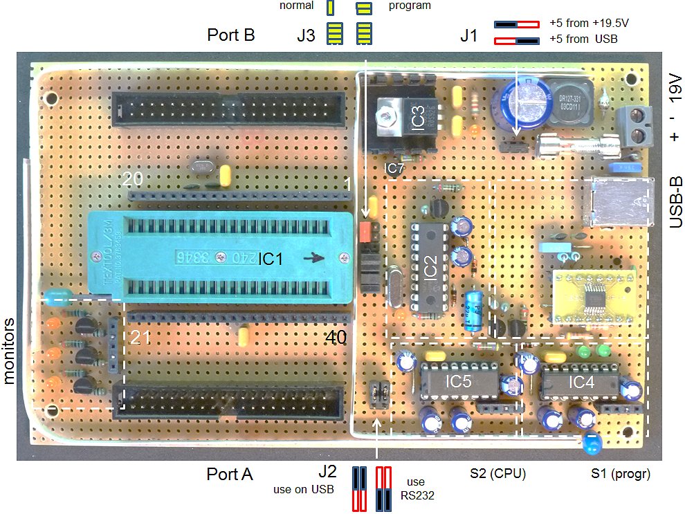
Figure 10.2. The CPU board
For the programing of the uTracer3 I used my trusted “Wisp648” PIC programmer designed by Wouter van Ooijen. I have used this programmer for years to my complete satisfaction. The programmer is so small and simple that I decided to include it onto the CPU board so that it doesn’t need to be connected to the separate programmer all the time. The programmer consists of a 16F648 (IC2) which uses a charge pump to generate the required 12 V programming voltage. The programmer has its own MAX232 (S1) for serial communication. Jumper J3 allows the 16F874 to be connected to the on-board programmer, the plug of my external programmer, or to run in normal mode.
In the uTracer3 a 7805 was used both for the 5V power supply, as well as for the reference voltage. This increased the number of calibrations necessary. For the new design I have included a real voltage reference in the form of an LM4040D50ILPRE50 (Mouser 595-LM4040D50ILPRE3). This is an integrated 5V precision reference in a TO92 envelope which simulates a zener diode. Resistor R13 biases the reference to a current of approximately (19.5-5)/4.7 kΩ ≈ 2.5 mA.
Port A and Port B will connect to two PCBs with the analog electronics, one board containing the anode and screen supply, while the other board will contain the grid and heater supply.

Parts of this page were written during our beautiful 2013 summer holiday to the Dutch coast in Cadzand in the extreme south west of Holland.
| to top of page | back to homepage |
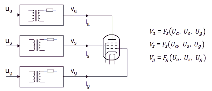
Figure 11.1 Schematic diagram of the uTracer4.
Figure 11.1 shows a schematic diagram of the uTracer4 limited to the essential blocks needed for this section. On the left hand side we start with three input voltages Ua, Us and Ug, with the subscripts obviously standing for anode, screen and grid. These three input voltages are subsequently “up converted” by transformers, resulting in the voltages Va, Vs and Vg which are applied to the tube, resulting in three currents Ia, Is, and Ig. The transformer unfortunately is a lossy component. This means that the ratio of the output voltage Vx/Ux is not constant and only depending on the transformation ratio, but it also depends on the current! The current(s) in turn are depending on the characteristics of the tube (which is unknown), and on the voltages applied to the tube: Va, Vs, Vg. In mathematical form we can write that each of the three voltages Va, Vs and Vg as a function of the voltages Ua, Us, and Ug (Figure 11.1 right). The question now is, which voltage triplet Ua, Us, and Ug needs to be applied in order to obtain the set-point values for Va, Vs, and Vg?
Since the characteristics of the tube are unknown, there is no way to analytically derive formulae for Ua, Us, and Ug. The best we can do is use an iterative scheme whereby the correct values are determined through a series of “educated guesses.” There are several way how this can be done. In this section I want to discuss what I think is the most plausible method at this moment. I am not sure how to continue from here. One possibility is to build the hardware and to test the algorithms, the other possibility is to simulate the hardware using models for the
hardware and the tube, and in this way to study and test the algorithms.
Linearization
To improve the readability of this section we will use a kind of shorthand writing whereby U represents the vector U = (Ua, Us, Ug, and V the vector V = (Va, Vs, Vg). In the simplest scheme, we just try different values for U until the resultant V is close enough to the desired set point value Vset. If we had only one knob to turn, that would not be so difficult, however, in this case we have three knobs to turn (Ua, US, Ug), and each of these knobs influence each other! So we need to have some kind of clever method to reduce the number of “guesses”. A possible suitable method is through linearization of the problem.
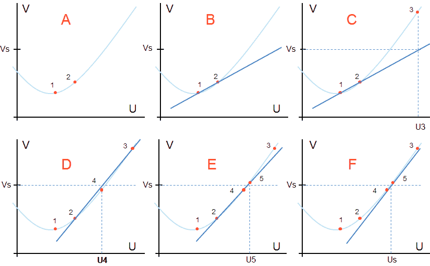
Figure 11.2 Finding your way on an unknown curve in one dimension by linearization.
Figure 11.2 recalls the idea behind linearization. Suppose that we have some kind of transfer curve, indicated by the lightly colored line. We do not know the shape of the curve, but by applying a voltage U to “the device” we can obtain the corresponding value of V. We furthermore know that the curve does not contain any strange features such as discontinuities or singularities. We start the iteration procedure by making two best (“educated”) guesses for U. These points are indicated in Fig. 11.2A as points 1 and 2. Through these two points we now construct a straight line (Fig. 11.2B). With this straight line known we can now derive a better guess for U, and testing this value of U will give a new point on the curve (point 3), which is hopefully a bit closer to the desired set-point value (Fig. 11.2C). The whole procedure is repeated again with the two points which are now closest to the set-point value (Fig. 11.2D). Note that this doesn’t automatically imply the last two points! In Fig 11.2E e.g. the line is constructed through points 2 and 4, resulting in point 5. The procedure is repeated until abs(V-Vset) < error.
This simple example illustrates the linearization method for only one dimension. In two dimensions, a three dimensional landscape of hills and values is approximated by a flat plane. In this case we need three best guesses. Also in three dimensions the same procedure can be used, be it that it is very difficult to imagine “a three dimensional flat space”! Nevertheless, the math works just fine. Note that in this case we need (in principle) four best guesses!
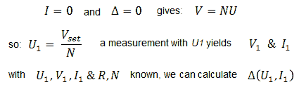
So in the vicinity of the point of interest, we can linearize the unknown equations of Fig. 11.1 as:
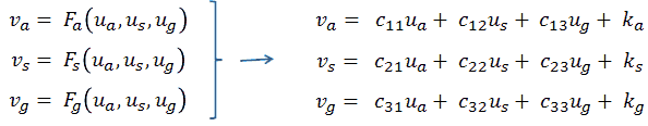
Using the “shorthand” matrix notation:
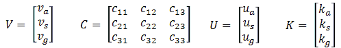
This can be simplified to:
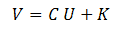
We now use our knowledge of the system to simplify this a bit. We know that when U=0 (Ua=0, Us=0, Ug=0) the output voltages are zero, so V=0. This means that the constants Ka, Ks and Kg in the linearized equations are 0, so K=0. The equation now reduces to:

With the elimination of the constant term, we only need three points to fully determine C. The iteration process therefore starts with a “list of points” containing three “best guess” points = {(U1,V1) (U2,V2), (U3,V3)}. How these points can be obtained will be discussed later.
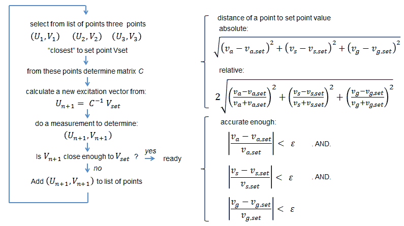
The iteration process is straightforward and closely follows the iteration process for one variable that was outlined above. We start with a list of points. At the start this list will only contain three points: “the best guesses”. During the course of the iteration process, the list of points will grow. From the list of points three points are selected which are “closest” to the set point voltage vector. These three points are used to linearize the transfer function resulting in matrix C. Using the inverted matrix C now a new vector Un+1 is obtained. Voltages Un+1 are set in the hardware and a new measurement is performed resulting in voltages Vn+1. At this point it can be that Vn+1 is already accurate enough. In that case the iteration process is stopped. If Vn+1 is still not accurate enough (Un+1,Vn+1) is added to the list of points, and a new iteration loop is started.
“Closest” is hardly a mathematical term, but the figure above shows how the distance between a certain voltage (vector) and the set-point voltage (vector) can be defined. We can calculate the distance in absolute value, but in that case higher voltages will be dominant over the lower voltages. It therefore is perhaps a good idea to weight the voltages differences by the average values, so that a relative distance is obtained. For the stop criterion we simple calculate the relative error of the three separate voltages. When the relative error of all three voltages is smaller than a certain value, the iteration process is stopped.
Calculating matrix C
Calculation of matrix C from three points is straightforward and really high-school stuff. Nevertheless, just for completeness and documentation here is how determination of C reduces to the solving of three sets of equations which can be solved by a simple Gaussian elimination procedure:

In order for the solver strategy described above to work fast, it is important that the starting points are close to the final solution. There are several ways to generate a suitable set of starting points. One strategy could be to start from the previous measurement point on the curve. We will talk about this possibility later. However, when it is the first point on to be measured, no data at all is available. In that case we can use our knowledge of the system. We know that the output voltage of the transformers with reasonable precision can be written as:
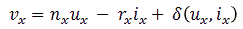
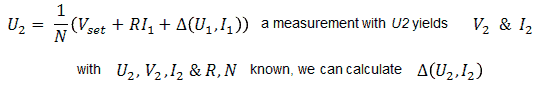
With n the transformation ratio, r the equivalent resistance of the transformer referred to the output, and i the output current flowing to the tube terminal. Unfortunately there is always a small error we make due to non-linearities in the circuit or losses which can not be accounted for by r. In the above equation these inaccuracies are accounted for by the error term δ(u,i), which – as indicated - in general is a function of the bias conditions.

My hesitation stems from the fact that in case the currents are very small, or negligible, especially the last two points will almost coincide because I=0 and Δ was determined during the first measurement, so that the three points are not very suitable as a base for a reliable linearization. On the other hand, it can very well be that in case the currents are very small, the set-point value for V is already reached during the first three guesses. After every guess it is therefore necessary to check if the “guessed point” satisfies the accuracy criterion.
So far we considered the general case where we have three variable voltages Va, Vs, and Vg, which all three have to be set within the specified accuracy. In practice this is not always necessary. First of all obviously when triodes are tested, and no screen voltage is needed. The fact that one variable less has to be optimized will considerably speed up the iteration process. On top of that the grid bias will be negative in most cases so that there is no grid current and the grid voltage can be very accurately predicted!
Next to this there is no need to accurately set the first or “running” variable (this is the variable which is plotted along the x-axis), as long as it is accurately measured. People who have ever worked with a Tektronix curve tracer will immediately understand what I mean. Let’s take the tracing of a set of pentode output characteristics as an example. For a particular curve in the set of curves, it is important that the grid and screen voltages are accurately set, but there is no need to accurately set the anode voltage, as long as it can be accurately measured and plotted in the graph. Suppose e.g. that between 0 and 300 volts 10 points need to be plotted, in that case it is sufficient to more or less guess the voltages so that approximately 30 V intervals are obtained.
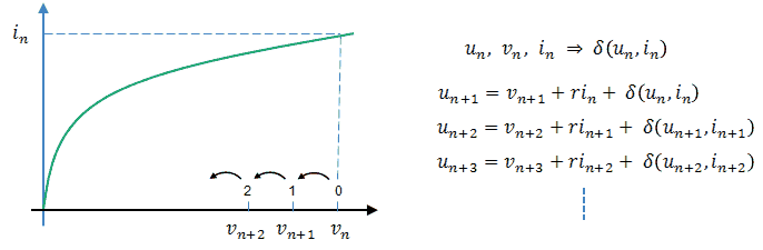
| to top of page | back to homepage |
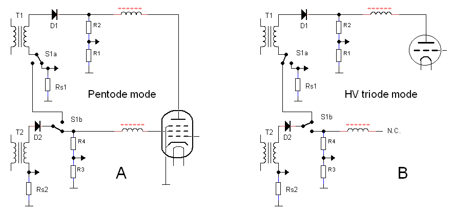
Figure 12.1 In normal “pentode mode” the two high voltage pulse supplies are used independently (A). In the “high-voltage” triode mode the two supplies are stacked so that the double output voltage is obtained (B).
As explained in section 6 each supply is designed to deliver at least 650 V at 300 mA, while the maximum output voltage can increase to 800 V for lower currents. It was also explained that one of the great advantages of using a boost transformer is that the secondary winding of the transformer is floating with respect to the rest of the circuit. This makes it possible “to stack” windings so that the double output voltage can be obtained. Figure 12.1 shows the principle of the circuit I have in mind. In HV-triode mode the output voltage is measured by the resistive voltage divider R1/R2. This divider thus should be able to withstand peak voltages of 2 kV and reduce it to a safe 5 V. A problem is the high voltages switch S1. Although this switch doesn’t have to switch high voltages or currents, it should have a dielectric isolation of at least 2 kV. Perhaps the use of a relais instead of a switch would be a far better solution altogether since this would also eliminate the tricky high voltage wiring to the panel of the instrument. I didn’t do a thorough search for a suitable relais yet, but a simple and cheap relais like the
G5LA-1E 5DC from Omron (Farnell 1455506) already seems to do the trick. For the diodes 2 kV blocking types should be used, or 1 kV types with a high resistive bleeder resistor in parallel to properly distribute the blocking voltage.
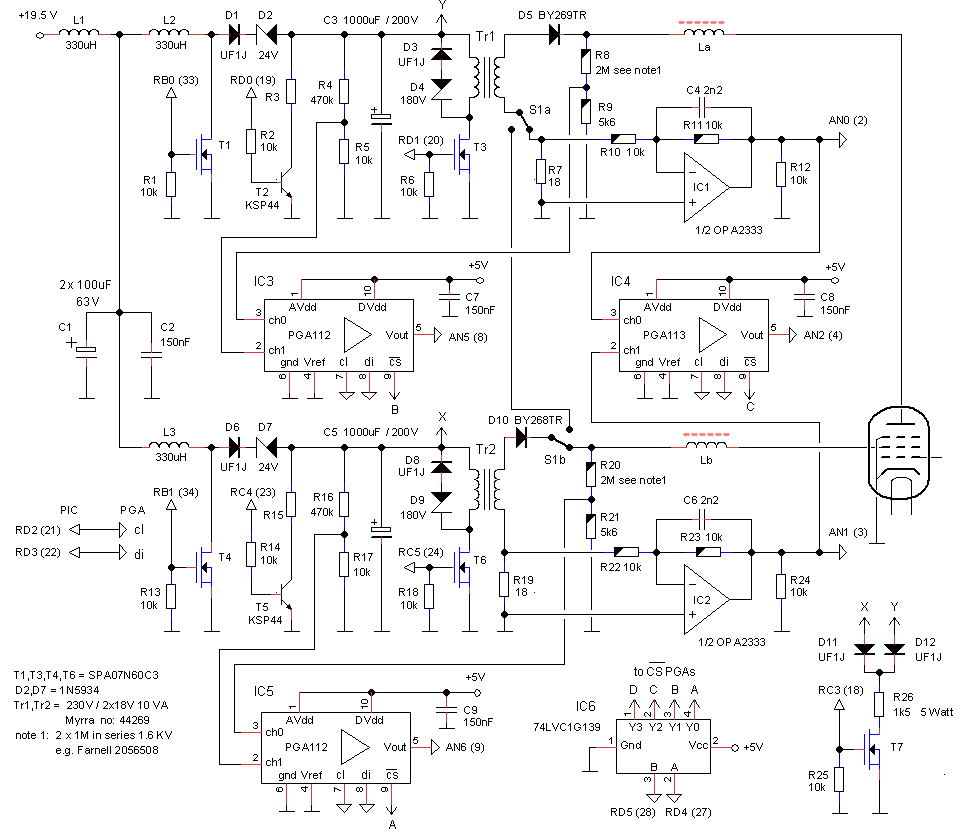
Figure 12.2 Detailed circuit diagram of the anode/screen supply section.
Figure 12.2 shows the detailed circuit diagram of the anode/screen supply section. The circuit basically consists of two identical circuits shown in Fig. 8.4. Looking at the anode section T1, D1, L2 and C3 form the actual boost converter itself. Zener diode D2 only starts conducting when the sum of the supply voltage and the fly-back voltage of L2 exceed 24V. This simple trick allows the voltage across C3 to be regulated down to 0 V. D3, D4 and D5 ensure a quick “discharging” of the transformer after the measurement pulse. For the reservoir capacitor C3 in first instance a 1000 µF / 400 V type is chosen. A disadvantage of such a high capacitor value is that it charges and discharges rather slow. Experiments will point out if a smaller 470 µF capacitor is also sufficient. Transistor T2 in combination with R3 discharge the reservoir capacitor in case the capacitor voltage is too high. The value of R3 is too high to quickly discharge C3 e.g. after a measurement has been completed. Therefor an additional “quick discharge” circuit was added consisting of D11, D12, R26 and T7. This simple circuit discharges the anode and screen reservoir capacitors simultaneously, dumping the energy into a 1k5 / 5 W resistor which can get rather warm in the process!
One of the short comings of the uTracer3 is that especially in the low voltage regime the resolution of the voltage setting is rather poor as a result of the limited resolution of the ADC. This is one of the reasons why for the uTracer4 also Programmable Gain Amplifiers (PGAs) are used for the voltage measurements. Another reason is that the multiple input PGAs increase the number of AD channels which is needed because for the uTracer4 both the input as well as the output voltage of the transformers needs to be measured. During the charging phase channel 1 of IC3 and IC5 is selected while during the measurement pulse channel 0 is selected. This series of PGAs come in four flavors: 2 or 10 inputs and binary gains or “oscilloscope gains” (1x, 2x, 5x, 10, 20x etc.). For the voltage measurements binary gain PGA are used, for the current measurments “oscilloscope gains”.
The reason why two 2-input PGAs were used instead of one 10 input is that this would require extremely fast switching between the inputs during the charging phase when every 100 us another boost converter is sampled.
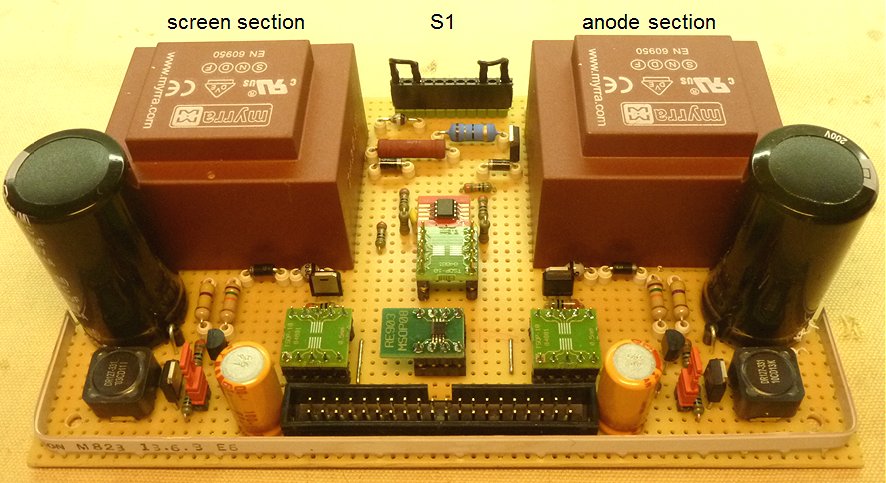
Figure 12.3 The anode and screen power supplies on perf-board.
The current sense circuit is basically the same as for the uTracer3, however in this case a modern single 5 V supply OpAmp is used. The OPA2333 houses two OPA333 OpAmps in a single SOIC package. The OPA333 is a single supply OpAmp with an offset voltage of less than 10 µV. A special feature of the OPA333 is that, with the aid of a load resistor to ground, the output voltage can be as low as several µV which is necessary in this circuit. The only disadvantage of the OpAmp is the relatively low slew-rate of 0.16 V/µs, which is a bit on the low side for this application. With only a single 5 V supply voltage there is much less need for the extensive clamping protections used in the uTracer3, which greatly simplifies the layout of the circuit. On the input side of the OpAmp and PGAs I have chosen to rely on the clamping diodes in the ICs which is perfectly allowed on condition that the current is limited to the maximum current specified in the datasheet (10 mA). Both channels share one PGA113. During the measurement pulse when the currents are measured there is enough time to switch between the different channels. Possibly in the final circuit a single PGA117 with 10 channels can be used to also measure the grid current and some other voltages like the supply voltage.
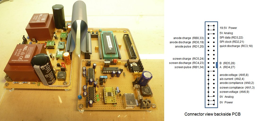
Figure 12.4 The high-voltage supplies connected to the CPU board and the connections to the 40-pin box header connector.
Figure 12.3 shows the build of the circuit on a piece of perf-board. The implementation is rather spacious to allow for easy probing. Compared to the uTracer3 the transformers look huge and heavy, they are! The good thing is that they are readily available and very cheap. What I learned from making the uTracer3 kit was to reduce as much as possible the number of different components. For the MOSFETs again the SPA07N60 was used but, since they do not get warm anyway, this time in a much slimmer TO-262 package. The anode/screen supply board is connected to the CPU board via a 40 pin connector (Fig. 12.4). Components which carry high-voltages were mounted using a ceramic spacer for the sole purpose of warning me of their lethal voltage during debugging and testing. The selection between “pentode mode” and “HV triode mode” is made via a simple wired connector where a pin distance of 5 mm was used to provide the necessary isolation (Fig. 12.5). The problem with this circuit is that is absolutely doesn’t do anything without the proper software. So the next job will be the firmware. This has to be done is steps. The first step will be to adapt the interrupt service routine which charges the reservoir capacitors to the desired set point value.

Figure 12.5 a simple connector is used to select between “pentode” or “high-voltage triode” modes.
| to top of page | back to homepage |
Now that a large part of the hardware of the test setup has been completed, the next job is start bringing it to life, in other words: the firmware. One way or the other it always takes me a day or so to mentally switch from soldering to programming. Fortunately some parts of the firmware of the uTracer3 can be re-used so that I didn’t have to start all over from scratch. The first thing that needed to be brought on-line were the high voltage supplies, in other words: the interrupt routine which controls the boost converters, and the routines which control the interrupt routine.
Let’s shortly recapitulate the working of the high-voltage supplies. When the reservoir capacitor voltage is lower than the set-point value, an interrupt service routine generates every 100 µs a 30 µs pulse which switches-on the transistor in the boost converter. After every pulse a package of charge is “injected” into the high-voltage electrolytic reservoir capacitor increasing its voltage. When the desired set-point voltage is reached the pulse rate is reduced only to replenish the charge that is leaking away so that a constant capacitor voltage is obtained. On the other hand, when the capacitor voltage is higher than the set-point value, the reservoir capacitor is discharged into a resistor by switching on the discharge transistor until the voltage drops below set-point value after which the boost converter is switched on again so that the set-point value is maintained. For a number of reasons the control of the discharging in the uTracer3 was not included in the interrupt routine, but separately implemented in the main program.
For the uTracer4 I wanted to improve the high voltage supplies with respect to three points:
Integrating discharging in the interrupt routine
For the uTracer3 an interrupt driven boost converter control system was developed that can simultaneously control up to eight boost converters running in the back ground of the PIC. The principle (Part I) and the implementation (Part II) of that system are described on the uTracer3 weblog page, and interested readers are referred to those sections for background information.
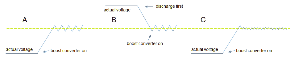
Figure 13.1 When the actual voltage is higher than the new set-point value the reservoir capacitor first has to be discharged (B). Trickle charging (C)
For the uTracer4 I wanted to include the complete control of the boost converters (charging and discharging) into the interrupt routine without the need to worry about boost converter details at all in the main program. Remember that the boost converter control algorithm for the uTracer3 was very simple: pulse the converter when the output is too low, and do nothing when the set-point is reached (Fig. 13.1 A). With the discharging integrated into the interrupt service routine, we have deal with the situation that the initial capacitor voltage can be too high. In this case the reservoir capacitor has to be discharged first, before the normal procedure as described above can be resumed (Fig. 13.1 B). To realize this a new flag (BST_SET) is introduced which has to be set by the main program when a new set-point value has been loaded.
The boost converter interrupt routine is controlled by the main program by means of a number of flags. For example a boost converter is enabled by setting the BST_ENBL flag. The interrupt routine can control up to eight boost converter simultaneously. So conveniently, The BST_ENBL flags have been arranged in one byte. In this way all the control flags are organized in a series of bytes, with a certain bit number corresponding to a certain boost converter.
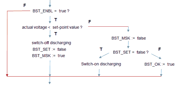
Figure 13.2 Flow diagram of the interrupt service routine with integrated discharging.
The flow diagram for the algorithm controlling a boost converter is shown in Fig. 13.2. When the boost converter is not enabled no decisions are taken what so ever. When the boost converter is enabled, the converter is always pulsed when the output voltage is too low. When the output voltage is too high (or high enough), and a new set-point value was loaded, the reservoir capacitor is first discharged before normal operation is resumed. If a new set-point value was not loaded normal operation is assumed and the BST_OK is set to indicate that the desired voltage is reached. The fragment of assembler code shown in Fig. 13.3 gives the correct sequence by which a new set-point value is loaded into the boost converter. After new set-point values have been loaded the output voltages have reached their set-point values when all BST_OK flags are set. The fragment of assembled given below illustrates the correct way a new set-point value has to be set, and the order in which the flags whch are involved have to be set or reset.
set_anode:	bcf		BST_ENBL,ANODE	;disable anode boost converter
		anode_discharge_off			;just to be sure
		movlw		000H			;set anode supply to 50V
		movwf		BST_AVS_H		;
		movlw		02BH			;
		movwf		BST_AVS_L		;
		call		delay_1ms		;stabilize int. routine (just to be sure)
		bsf		BST_LONG,ANODE	;long boost converter pulses (in this example)
		bcf		BST_OK,ANODE		;reset OK flag
		bcf		BST_MSK,ANODE	;reset MSK flag
		bsf		BST_SET,ANODE	;to signal that a new value has been loaded
		bsf		BST_ENBL,ANODE	;enable anode boort converter
Improving the resolution and accuracy at lower output voltages
The ADC on board of the PIC has a 10 bit resolution. This means that for a total input voltage range of 200 V the resolution amounts to 200 / 1024 ≅ 0.2 V. For high voltages that is quite good; at 200 V for example a step of 0.2 V amounts to 0.1 %. However, for lower voltages the relative resolution dramatically decreases. At 5 V output voltage for example the relative resolution is only 0.2/5 = 0.04 or 4%. For the uTracer3 that was not such problem, however, in the uTracer4 the voltage is up-transformed by a factor of about 7 so that a higher resolution at lower voltages is needed. There are basically two ways to realize this: 1. Use an ADC with a higher resolution, 2. use a Programmable Gain Amplifier (PGA) in front of the ADC to bring the input voltage of the ADC to “full scale.” With the progress in miniaturization of high performance ADC with integrated voltage references the first option is becoming more and more attractive (just have a look at the MCP3421), however, the interrupt based software control of the boost converters requires some tricky and fast interfacing with the ADC which is more easily done when the ADC is “on board.” For that reason I decided to use the second option of using a PGA in front of the ADC.
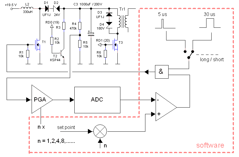
Figure 13.3 Schematic overview of the boost converter control in hard- and software.
Figure 13.3 shows the basic configuration and control loop of a single boost converter, whereby the part within the red dashed line is implemented in software (the discharging part of the software is not shown here). The PGA used here is a PGA112. The gain of this PGA can be set to binary values (1x,2x,4x,….,128x). The idea is that the input voltage of the ADC is always such that it is preferably in the upper half of the input voltage range of the ADC. For the ADC on board of the PIC this means that preferably the input voltage should be somewhere between 2.5 and 5 V (the most significant bit “1”).
The way this is implemented is very simple. In contrast to the uTracer3 where just 10 bits were used to set a voltage, here the full 16 bits are used. Whereas in the uTracer3 the output format of the ADC was “right justified,” in this case the output format is “left justified” so that when the input voltage of the ADC is in the upper half of the input voltage range, the most significant bit of the two bytes (bit 15) is “1”.
	Gain := 1
	Do While (MSB = 0).AND.(Gain =< 128)
		Gain := Gain * 2
		rotate both bytes of SET_POINT left  (multiply by 2)
	End Do
The simple algorithm above checks if the MSB bit of the 16 bit set-point value is “1”. If not, both the gain as well as the set point are multiplied by a factor 2, until either the MSB bit becomes “1”, or the maximum gain of the PGA (128x) has been reached. Multiplying the set-point value by a factor of 2 is easily done by rotating the bits in the two bytes which hold the set-point one position to the left. Note that by multiplying the input signal of the ADC, and the set-point value by the same factor the output voltage remains the same. The formulae below give the relation between the 16 bit two-byte set-point value and the output voltage.
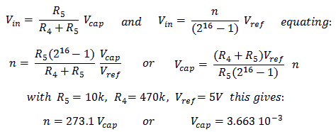
Long and short boost converter pulses & time-out error handling.
The second effect which loweres the accuracy at lower voltages is related to the very nature of a boost converter. Every time the boost converter is pulsed, a package with a constant amount of charge is injected into the reservoir capacitor resulting in an increase of the capacitor voltage. This voltage increment is normally quite small, and depends on the amount of charge already in the capacitor, and the capacitor value (read more about it in the uTracer3 weblog). As described in the uTracer3 weblog, these increments become smaller as the capacitor voltage increases, and for higher voltages they soon become negligible. However, for low voltages the voltage increment of a single boost converter pulse can be quite noticeable. Figure 13.4A shows the capacitor voltage when the output voltage is set to 6.5 V with the standard pulse length of 30 us and a PGA gain of 1x (The DC component was removed by placing a 1 uF capacitor in series with the 1 Mohm input of the scope). As can be seen, despite the fact that a rather large capacitor value of 1000 uF is used, the voltage fluctuations can easily be large as 200 mV.
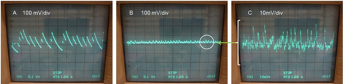
Figure 13.4 AC component of the capacitor voltage using: long (30 us) pulses and PGA 1x gain (A), short pulses (5 us) and PGA automatic adjust (B).
Traces (A) and (B) are taken with 100 mV/div, Trace (C) is identical to (B) but now with 10 mV/div.
The boost converter fluctuations can be reduced by using shorter boost converter pulses. This will reduce the energy build-up in the inductor, and thus the amount of energy (and voltage) increase of the reservoir capacitor. Already in the uTracer3 boost converter interrupt routine a provision was implemented to use both long (for fast charging), as well short pulses (for accurate voltage). In the final program this option was not used however, because it was felt that it was not really necessary because I thought that very low boost converter voltages were not going to be used anyway. “Unfortunately” then somebody had the idea to use the screen supply for positive grid biases and all of a sudden a very accurate output voltage did become important!
Since in the uTracer4 the discharging mechanism was integrated in the interrupt service routines, it became possible to combine long pulses (30 us) for fast charging with short pulses (5 us) for accurate charging in quite a straightforward way. The basic idea is to first call the routine which charges the capacitor with long pulses in the standard way until the set-point value is reached (actually just exceeds). Next, exactly the same routine is used with exactly the same set-point value but now with short pulses. The routine will first perform a very short discharge until the capacitor voltage drops just below the set-point value after which the capacitor will be re-charged, but now with short pulses (Fig. 13.1C).
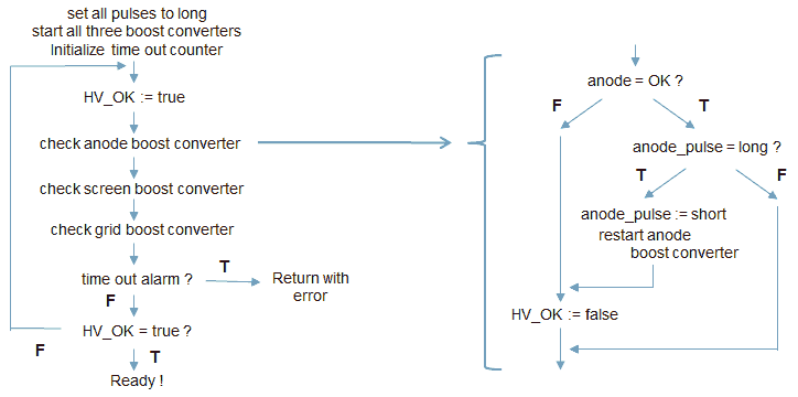
Figure 13.5 Flow diagram of the “set-hv” routine which takes care of the combined long/short pulse charging of the reservoir capacitors.
The flow diagram of Fig. 13.5 illustrates how the complete algorithm is implemented. First the pulse length is set to long, and all three capacitors are charged to their nominal set-point value and the flag “HV_OK” is set true. The charging progress in monitored in a loop in which the charging of the three reservoir capacitors is controlled by three identical pieces of code, illustrated by the flow diagram for the anode. When the “BST_OK” flag becomes set, the algorithm checks if the “BST_LONG” flag was already reset. If not, it resets the “BST_LONG” flag and restarts the charging process, but now with short pulses. Only when the “BST_OK” flag was set while the capacitor was charged with short pulses the “HV_OK” flag is not reset. The loop ends when the “HV_OK” flag is still set after servicing all three capacitors, or when there is a time-out.
The time-out timer is implemented as a simple piece of code at the end of the interrupt service routine which, when enabled, decrements a 16 bits counter upon every call (100 us). When the counter reaches zero an alarm flag is set. The main program sets the counter to 3 sec at the beginning of the capacitor charge routine and enables the timer. When the alarm flag is set before the capacitors are charged (with short pulses) the loop terminates with error code “00010xxx”, in which “xxx” are the three LSB bits from the “BST_OK” byte. In this way we know which capacitor failed “to get on-line.”
On second thoughts …
The material in this sub-section was actually written after the next section was completed. During the testing of the “adaptive pulse length” algorithm discussed in the next section something peculiar was discovered. To test the algorithm, 100 pulses were fired and the amplitude of every pulse was recorded for statistical analysis. Strangely enough, whereas normally all the pulses had the same amplitude within a fraction of a percent, it turned out that the first pulse in a series of pulses was always a few percent lower than the other pulses.
At first I tried to ignore the phenomenon, but soon realized that if this was some kind of a random error, it would play havoc with the iteration algorithm. In the end it resulted in quite an extensive investigation into the source of the problem.
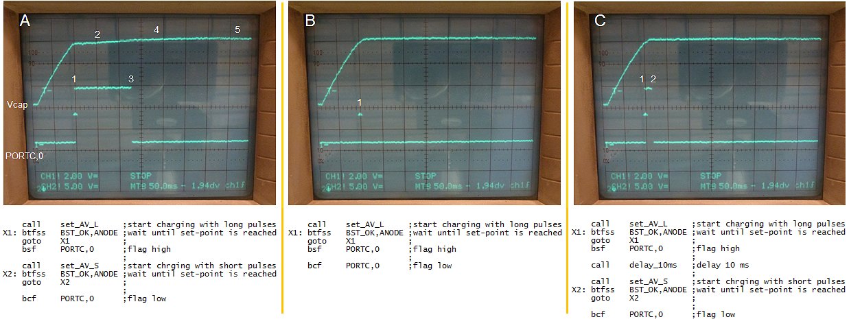
Figure 13.6 Zooming in on the charging problem
The problem only occurred when the reservoir capacitor was charged from a low voltage to a higher voltage. After a lot of searching it turned out that in that case, when the “set-hv” routine indicates that the set-point voltage is reached, it is in fact not! Figure 13.6A shows the phenomenon in its simplest form using the piece of code listed below the photograph. The upper trace shows the reservoir capacitor voltage. The lower trace shows I/O pin PORTC,0 which is used as a flag to keep track of the execution of the code. The code shows the simplest implementation of the algorithm shown in Fig. 13.5. The program first starts by “fast-charging” the reservoir capacitor using long (20us) boost-converter pulses. When the flag “BST_OK,ANODE” becomes high, the interrupt service routine signals that the set-point value has been reached (point 1 in Fig.13.6A). At that point, just to have a reference point PORTC,0 is made high (see lower trace), and the “slow charging” starts. The remarkable thing now is that, although the fast charge routine indicated that the set-point was reached, there is still significant charging during the slow charge phase (point 2 Fig.13.6A). The same thing happens when the slow charge routine signals that the set-point value has been reached (point 3 Fig.13.6A). The interrupt routine now in principle only needs to
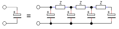 maintain the set-point value, but instead we still observe a continued increase of the capacitor voltage (point 4 Fig.13.6A). Only after several hundreds of milliseconds the final plateau value is reached (point 5 Fig. 13.6A). Confused? Well I was!
Figure 13.6B shows a piece of the puzzle in solving the mystery. In this case the whole slow-charge part of the code was removed. The behavior is now completely different. It seems as if the capacitor is directly charged to its final value as expected. However, close inspection reveals that the interrupt routine already 10-20 milliseconds before the capacitor voltage reaches its plateau value signals that the set-point voltage is reached (point 1 Fig.16.6B = trigger point). It appears that the capacitor voltage immediately after a boost converter pulse is higher than a few milliseconds later. For me the best way to imagine how that is possible is to view an (electrolytic) capacitor as being a distributed device that can be thought of as consisting of multiple capacitor sections connected small impedances (resistive and inductive). The effect of a boost converter pulse will be that it charges the capacitor closest to the terminals, but that the pulse is too short to make sure all the other capacitors are evenly charged. So what will happen in the time in between the boost converter pulses is that the excess amount of charge on the first capacitor will smear out over the others resulting in a drop in voltage at the terminals.
The simplest solution to solve this problem is to build in a delay after the interrupt routine has signaled that the set-point is reached. This will give the capacitor some time to equalize the charge over “all capacitors.” Figure 13.6C shows how the insertion of a short 10 ms delay in between the fast and slow charge routines completely changes the charging behavior (as compared to Fig. 13.6A). As it happens the algorithm for the “set-hv” routine now becomes a lot simpler (Fig. 13.7). The three boost converters are set to long pulses and enabled. The routine now simply waits until all three boost converters signal that the set-point value has been reached. At that moment a delay of 10 ms is inserted. Next the boost converters are set for short pulses and again enabled. When all three boost converters signal that the set-point voltage is reached the system is ready to fire a measurement pulse!
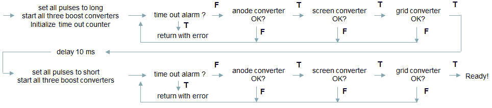
Figure 13.7 Revised flow of the “set-hv” routine.
Error signaling
When the boost converters reach their set point values within the time-out period, the “set-hv” routine exits with the carry flag and W cleared.
When there is a time-out error, C is set, and W = 00010xxx, with xxx the three lower bits of “BST_OK”. When one of these bits is “0”, the corresponding boost converter failed to charge the capacitor to the set-point value.

Figure 13.8 Error signalling.

One of the most pleasant aspects of working one day a week at the Technical University of Delft, is that on my way from the railway station to the University I pass the exact spot from where Johannes Vermeer painted his world famous “view on Delft.” Reproductions and photographs of this painting fail to reproduce the unforgettable impression and sensation it causes when viewed in reality. It is a must see whenever you are in The Hague where it is on view in “Het Mauritshuis.” For a great Dutch site about the painting click here.
| to top of page | back to homepage |
First let’s review some of the theory from sections 4 and 5. When the transformer is unloaded, a rectangular pulse on the primary side of the transformer will translate into a nice rectangular pulse at the secondary side. It was demonstrated that in order to avoid saturation, the maximum pulse length * amplitude product of the input pulse for the particular transformer used in these experiments should not exceed 162 msV. When the transformer is loaded, the situation changes dramatically. As a result of the leakage inductance, the slope of the trailing edge of the output voltage pulse will decrease drastically. Figure 5.5 illustrates the change in shape of the output pulse when the load is increased. Since the voltage drop over the leakage inductance lowers the voltage over the magnetization inductance, the maximum pulse length that can be applied before saturation of the core occurs can now be longer. Using a fixed pulse length doesn’t utilize the full potential of the transformer concept. A short pulse limits the use to low currents because for higher currents it is too short to reach the plateau value. A longer pulse on the other hand is fine for higher currents, but it will cause the core to go into saturation for higher voltages! The answer is an adaptable pulse length algorithm, which adjust the pulse length in such a way that the pulse is terminated when the output voltages reaches the plateau value.
Figure 14.1 The adaptive pulse length algorithm terminates the pulse as the plateau value is reached. The plateau is defined by the stop-criterion shown on the right.
The idea behind the adaptive pulse length is to sample the output voltage of the transformer during the pulse. An algorithm processes the samples and terminates the pulse when the relative difference between two consecutive samples becomes less than a predefined relative error η (Fig. 14.1). All this requires some very serious AD converting and math at full speed! We have found that in practice the pulse length can vary between 0.5 and 3 ms and that such an adaptive pulse length algorithm only makes sense if the samples are taken approximately every 200 µs. In between some – what seems like - floating point math has to be done, and on top of that there is not one pulse generator to consider, but three simultaneously (anode, screen and grid).
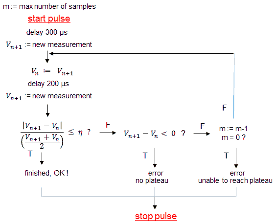
Figure 14.2 The basic elements of the adaptive pulse length algorithm.
The measurement pulse is generated and controlled by a subroutine appropriately called “Fire”! The simplified flow diagram of this routine is shown in Fig. 14.2. Note that the flow diagram for simplicity only illustrates one pulse generator, while in reality three pulse generators have to be controlled simultaneously. The routine first starts by preparing the hard- and software for the measurement pulse: the boost converters are switched off and interrupts are disabled. The PGA’s are programmed so that the output voltage is measured and the appropriate gain is selected. After these preparations the measurement pulse is started.
A fixed delay of 300 µs makes sure that transient and ringing effects associated with the switching on of the measurement pulse MOSFETs are ignored. After the delay the first output voltage sample is taken, and this “new” (Vn+1) sample is copied to “the previous” (Vn) sample value. After a sample delay of 200 µs a new sample is taken and the value of the new sample is compared to the previous sample value. If the relative difference between the samples is smaller than the maximum allowed tolerance, the pulse is terminated in a normal way. When the relative difference is larger than the specified tolerance, the routine checks if the value of the new sample is higher than the value of the previous sample. If this is not the case, it means that the plateau was so small that no stable output voltage could be obtained. In that case the pulse is also terminated but with an error condition. In case the pulse is still rising, the sample counter is decremented. When the counter reaches zero, the pulse has reached its maximum length and the pulse is also terminated with an error code to signal that the maximum pulse length was exceeded before the plateau value was reached.
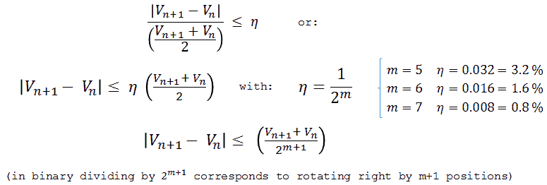
Figure 14.3 Calculation of the stop criterion.
So far everything is pretty straightforward. The calculation of the “stop-criterion” however, required some ingenuity and creativity. At first sight the calculation seems rather complex because it involves floating point arithmetic. However, with some trickery floating point calculations can be avoided, and the whole calculation can be done with only a few assembler instructions! The first step is to get rid of the division, by multiplying both sides of the inequality with the sum of the previous and the new sample values divided by two . The big trick now is to use for the “stop-criterion” η only special values namely the reciprocal of powers of two! So 1/2, 1/4, ..., 1/32, 1/64, 1/128. Note that 1/64, 1/128, 1/256 correspond to an error of 3.5%, 1.6% and 0.8% respectively! Not exactly round numbers, but who cares? The great simplification comes from the property of binary numbers that a division by a factor of two corresponds with shifting the bits in the byte (or word) one position to the right. The whole calculation of the stop-criterion is thereby reduced to additions, subtractions and some bit shifting.
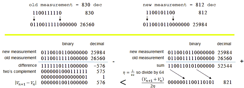
Figure 14.4 Example of the calculation of the stop criterion on bit level using two fictions sample values.
Figure 14.4 Shows in detail a calculation example for two samples with values Vn = 830 and Vn+1 = 812. Note that in this case the new sample value is lower than the previous sample value to demonstrate how the algorithm calculates the absolute value of the difference. The top half of Fig. 14.4 gives the binary presentation of 830 and 812. The ten bits from the ADC are stored in a 16 bit word in the way as shown in the figure. The PIC processor has the option to store the 10 bit result of the ADC left justified in the 16 bit result register. In this example the bits in the word are shifted right on bit, so that addition of two full scale (3FF) ADC results will not cause an overflow. Note that storing the result in this way boils down to multiplying the ADC result with 32! In the left part of Fig. 14.4 the left hand side of the inequality is calculated while the right part shows the calculation of the right hand side. The negative result from the subtraction is detected from the fact that the most significant bit of the result is “1”. The result is negated by taking the two’s complement (inverting all bits and adding one). On the right hand side the sum is shifted right 6 positions to realize a division by 64 (64=2*32, 2 for the average and 32 for %eta;=1/32=0.032).
Note that in this example the relative difference (2%) is smaller than the stop criterion (3.2%) so that the pulse can be terminated.
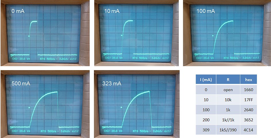
Figure 14.5 The adaptive algorithm at work for a 100 V output pulse under different load conditions.
Figure 14.5 shows the adaptive pulse length algorithm in action. The output of the pulse generator was connected to different loads resulting in pulses up to a current of 320 mA. For every load the boost converter voltage was adjusted so that the plateau value of the resultant output pulse was 100 V. At first sight the algorithm seem to work very nicely. For higher loads the trailing edge of the pulse decreases as expected and it takes longer before something which can be called a plateau is reached.
Figure 14.6 Statistical data of the output pulse under different load conditions and for different set-point values of the relative error η.
To get some statistical data on the performance of the algorithm, the hardware was programmed to fire a pulse every second. A very rudimentary interface between the hardware and the PC was made to record the last and the one but last sample value of every pulse. All data was recorded in a file and the program calculated some statistics which were collected in the table in Fig. 14.5. The purpose of the test was to find out “the actual flatness of the plateau” for a given set-point relative error. The relative error (η) was set to three different values 0.78% (1/128), 1.56% (1/64) and 3.13% (1/32). For each η different loads were applied to the output while the boost converter voltage was adjusted so that the output pulse amplitude remained constant at 100 V. The gain was set to such a value that the ADC was working in the upper half of its input voltage regime. The statistical values were calculated over 100 samples.
Listed in Fig. 14.6 are the average output voltage, the standard deviation of the output voltage, and the minimum and maximum deviation from the mean output voltage. The value of the output voltage itself is not so important because it depends on the boost converter voltage which was set manually. More important is the very small standard deviation and also the small minimum and maximum deviation. From the measured voltages also the relative error was calculated. The average relative error, the standard deviation on the relative error and the maximum relative error are shown in the last three columns of the table. As expected the maximum relative error is in all cases smaller than the set-point relative error. Even better, the average relative error is significantly less than the maximum value. Not surprisingly the relative error tends to increase for higher output currents as a result of the smaller slope of the pulse and the “vaguer” plateau.
Error signaling
It has already been mentioned before that, depending on the load conditions, the “fire” routine can fail to produce a set of stable output pulses. This can especially occur in the situation that the anode is heavily loaded, resulting in a long pulse because of the anode channel, while at the same time one of the other channels which is not heavily loaded goes into saturation. It is not only important that these fault conditions are detected, but also that they are reported back to the GUI. The three error conditions that can occur are:
Figure 14.7 Overview of error codes.
First Lines!
So far all testing was done with single pulses generated by the firmware itself. The next step was to connect the hardware to the GUI. For the time being the communication protocol between the GUI and the hardware was kept as much as possible identical to the protocol used for the uTracer3 so that the same software routines could be used. For the first tests the voltages entered in the GUI are the set-point voltages of the reservoir capacitors. The voltages and the currents displayed in the graph are the voltages measured at the output of the uTracer4. In the absence of a grid driver circuit a series of fixed resistors was used to test the behavior of the circuit over a wide range of voltages and currents.
Figure 14.8 First I-V curves using resistors as load.
Figure 14.8 shows the output current versus output voltage for an input voltage sweep between 5 and 200V. With open output the maximum output voltage is nearly 1000V. As expected the output voltage decreases with increasing load. Since the current sense resistor is 10 ohm, the maximum current that can be sensed is 5V/10 = 500 mA, and we find indeed that the current clips at that value. In the regime between 400 and 500 mA there are some abnormalities which need some further investigation, but below 350 mA the circuit behaves very nicely. At this point I am not sure how the spec the anode/screen output sections: simply define a maximum output current, or define a kind of operating area where the circuit can be used safely. Anyway, a conservative spec of 0-750V @ 300 mA seams quite feasible, while for lower currents voltages up to a 1000V, and for lower voltages currents up to 500 mA can be achieved. All in all a quite impressive for such a simple circuit! Just for myself a list of things to be done for the next steps:
| to top of page | back to homepage |
Most PhD students experience when they are about halfway their PhD project a period of emotional crisis that we sometimes refer to as the “PhD dip.” The initial euphoria over the start of the project and perhaps some initial positive results has subsided and the student finds himself (or herself) confronted with a labyrinth of problems that still needs to be solved, often combined with some pressure from a less empathic professor who is pushing the student to publish results which are not there yet. It is in the middle of such a crisis that I find myself at this moment with respect to this project. There are two events which may have triggered this “crisis.” It started with the realization that the “adaptive pulse length” idea described in the previous section does not really perform as expected. However, my doubt was completely inflamed by an email from Daren Kozey who expressed his doubts about the uTracer4 architecture as I am pursuing it at the moment.
Let’s review the main points that have made caused me doubting the present concept:

In conclusion I decided to stop with the uTracer 4 project for the moment and take the time to consider other options for higher voltages. This doesn’t mean that the transformer option is totally ruled out! It still has some very attractive features, but not in the form as where this project was going. Personally, for example, I would love to build a high-power triode tester, so a tester without a screen supply. That would simplify matters greatly. Please let me know your opinion about such a tester.
| to top of page | back to homepage |
When a constant voltage V is applied to a simple air coil with a certain inductance L a current will start to flow through the inductor. The current will obviously start at zero and then increase linearly according to I = (V*t)/L. Since the inductance of an air coil is usually very low, the current will increase very fast to the point where the current is limited by the resistance of the coil. At that point the current will remain constant at a value I = V/R.
When an iron core is inserted in the coil, the inductance of the inductor will increase by something like three orders of magnitude. What happens is that the magnetic moments of the individual iron atoms start to align with the external magnetic field so that the total magnetic flux is increased dramatically. Since the inductance is increased, the rate of increase in current when a constant voltage is applied will be much slower (I = V*t/L). At a certain magnetic field however, all the magnetic moments of the iron atoms are aligned, so that the metal core no longer can make a contribution to the increase in flux. This point, which is called saturation, occurs in iron at a magnetic field strength of typically 1.5 - 2.0 T. What is basically left after saturation of the core is an air coil with a very low inductance, resulting in a sharp and unwanted increase of the current.
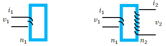
We now add a second coil to the iron core to make a transformer. Again a constant voltage is applied to the first (primary) coil, while the second (secondary) coil is left unconnected. As we have seen, the current and the magnetic flux will start to increase linearly at a rate given by I = (V*t)/L. The increasing flux will induce a voltage in the secondary coil which is proportional to the derivative of the flux increase to the time and to the ratio of the number of turns in the primary and secondary coils according to: V = (n2/n1) * dB/dt (Lenz law). So a constant voltage applied to the primary winding of a transformer will result in a constant voltage at the secondary winding of the transformer. Unfortunately this only holds for as long as the core is not in saturation. As soon as the core reaches saturation, it - from a magnetic point of view – disappears, resulting in a loss of magnetic coupling between the primary and secondary windings which in turn will result in a sharp drop of the voltage at the secondary winding, while the current in the primary winding will show a dramatic increase.
So, if we want to use a standard iron core transformer as a pulse transformer, it is important to avoid saturation of the core. To avoid saturation, the product of the amplitude of the voltage pulse and the duration of the pulse (remember I = V*t/L) will need to be kept below a certain maximum value. This value obviously depends on the inductance of the primary coil, but also on the properties of the iron that is used in the transformer, and on the way the transformer is constructed. Most of these details are unfortunately unknown for most transformers. So is it nevertheless possible to say something about this maximum V*t product? The answer is Yes! The reason is that manufacturers of transformers make their products as small, cheap and light as possible, and therefore design transformers in such a way that in normal use they just operate under saturation! It is this piece of information that we use to calculate the v*t product.
To explain how this can be done a bit of physics and math is unavoidable. The first physics law that we use is Ampere’s Law, which relates the magnetic field to current. In its most general form:
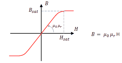
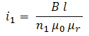
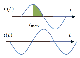
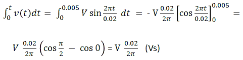

| to top of page | back to homepage |
In a transformer both the primary winding as well as the secondary winding have a series resistance. It is possible to combine these resistances to one equivalent resistance that is placed at either side of the transformer.
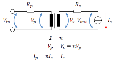
The figure above shows an ideal transformer with a turns ratio np : ns = 1 : n with a series resistance Rp at the primary side and a series resistance Rs at the secondary side. At the secondary side a load is connected to the transformer which “pulls” a current Is. The question now is, “what input voltage Vin do we need to apply to obtain an output voltage Vout.”
We simply calculate the output voltage taking into account the losses:
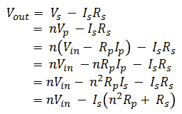
It is thus possible to define an “Equivalent Series Resistance” which is completely related to the secondary side of the transformer:
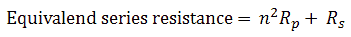
The required input voltage Vin for a given output voltage:
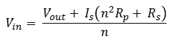
| to top of page | back to homepage |
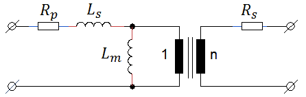
A transformer has many equivalent circuit models which all can describe the electrical behavior of the transformer equally well. The figure above shows a convenient circuit model of a transformer whereby all the inductances have been referred to the primary side. The transformer used in the example here is a SPITZNAGEL SPK 0801818. It is a small 10 VA PCB transformer with one 220 V winding and two 18 V secondary windings which I use in series. Since in this project the transformer is used the other way around as compared to normal I call the 36 V (2 x 18V) winding the primary and the 220 V winding the secondary winding. Measuring the component values is easy:
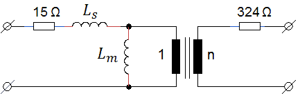
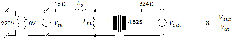
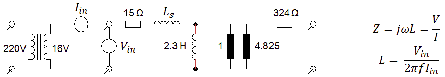
| to top of page | back to homepage |
During the work on section 7 (“The Morning After”) a rather strange phenomenon was encountered. I wanted to have a look at the negative “de-magnetization” pulse following the normal positive high voltage output pulse. The high voltage pulse has an amplitude of approximately 650 V, while the negative pulse which follows it has an amplitude of only a few volts (Fig. D1 A). The simplest way tho have a look at the small negative pulse was to simply increase the sensitivity of the vertical amplifier of the scope. In Fig. D1 B the sensitivity was increased by a factor of 100. The positive pulse is now completely off-scale, but the negative pulse has become visible. The negative pulse however, showed a completely unexpected wave shape.
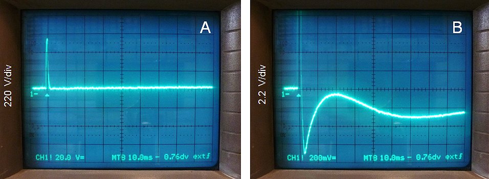
Figure D1 Positive pulse (A) and a magnification of the negative de-magnetization pulse following it (B)
At first I tried to find an explanation in some intricate interplay of the relative large inductances involved in the circuit. However, the absence of a capacitor large enough to explain the low oscillation frequency made this explanation unlikely. Finally, after gazing at the screen of the scope for an hour or so, it occurred to me that it might have something to do with the positive part of the pulse which is now completely off-scale. A simple zener/diode clipper which clips the positive part of the pulse to 5 V, confirmed the suspicion (Fig. D2). It just shows that it doesn’t hurt to always be critical to what instruments indicate.
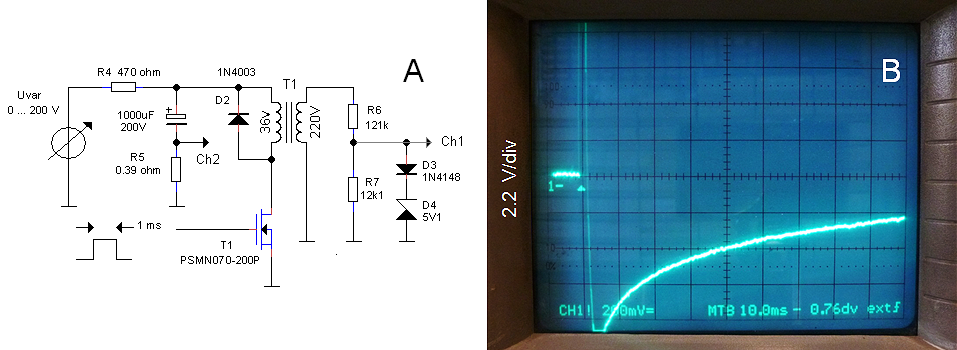
Figure D2 zener/diode pulse clipper (A) and correct representation of the negative de-magnetization pulse (B).
| to top of page | back to homepage |