
If you happened to stumble on this page by accident, a little explanation is in order. This page is a continuation of my first uTracer weblog page which discussed the development of a post-card size curve tracer: the uTracer. That page started of with a concept (the uTracer V1) which was abandoned halfway during the project. The second concept, as you can guess the uTracer V2, was completed to the end, and turned out to be quite a descent instrument. Since it had became rather difficult to find all the relevant information on the project in the weblog page, the project was summarized on a separate page which can be found here.
Although the version 2 uTracer works quite well, there is always room for improvement. I learned a lot from the V2 and identified a number of “weak points” which were summarized at the end of the blog . In the mean time I have a lot of new ideas to resolve the issues identified. This page therefore continues where the first page stopped, and will hopefully lead to the uTracer V3.
| to top of page | back to homepage | to part I |
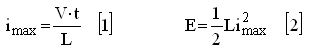
Most of the issues in the version 2 design are related to the way how the anode and screen currents are measured. Figure 2.1A summarizes the current measurement principle used or the version 2 design. The current is measured as a voltage drop over a series resistor in between the reservoir capacitor and the anode of the grid. By using a 1 uF high voltage “dropper” capacitor the pulse shaped drop over the series resistor is level shifted to ground for amplification and AD conversion.
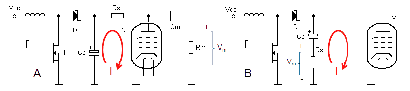
Figure 2.1 The old and the new current sense principles compared.
This construction has two enormous drawbacks. The first drawback is, that apart from the current pulse itself, in this way also the discharging of the reservoir capacitor is measured. Although, as explained in one of the previous sections, it is possible to compensate for this with an additional measurement, it is far from ideal and likely to introduce errors (more info). The second drawback is when the anode (or screen) voltage is increased or decreased; this will also induce a current in the dropper capacitor. It will take some time for the current through the dropper capacitor to return to zero and before the voltage over it becomes constant. So after the boost converter has charged the reservoir capacitor to the desired set point, the boost converter changes to “maintain voltage” mode for a few hundred milliseconds. What I had completely overlooked was that the boost converter pulses in the “maintain voltage” mode can result in significant fluctuations of the reservoir capacitor voltage, especially so for relatively low voltages (more info). This translates back to noise in the current values at low voltages. The solution was to switch the boost converter completely off during the stabilization interval. However, in that case the reservoir capacitor will start to discharge which, although it goes only very slowly, introduces drift. Now of course it is possible to compensate for this, but things become nastier every time. So it became time for a complete revision of the whole measurement principle!
The idea for improved measurement principle discussed in this section was induced by an email from René Schmitz from Germany. The idea is very simple and elegant. It is based on the notion that during the measurement the boost converter is switched off. So the only current flowing through the reservoir capacitor during the measurement pulse is the current through the tube. In that case the current sense resistor can be placed in the ground lead of the reservoir capacitor (Fig. 2.1B). This has the enormous advantage that the voltage over the resistor can now be measured directly with respect to ground without the need for the troublesome dropper capacitor. Additionally in this way only the current is measured and not the discharging of the dropper capacitor! Since the voltage is directly measured with respect to ground it is much easier to amplify the voltage drop over the resistor so that a smaller resistor value can be used. A very attractive idea is to replace this OpAmp with a Programmable Gain Amplifier such as the PGA103 from Burr-Brown of the MAX9939 from MAXIM.
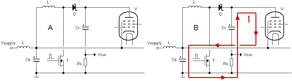
Figure 2.2 By raising the cathode potential to the power supply voltage, the anode to cathode voltage can be varied starting from zero.
Another drawback of the V2 uTracer was that the lowest voltage that the anode and screen boost converters could generate was equal to the supply voltage, so in this case 19.5 V. This means that the output curves (Ia(Va)) can only be taken starting from 19.5 V. At first I didn’t think that this was such a big deal, but looking at the curves, I cannot help thinking that an important part of them is missing. Since the output of a boost converter is directly connected via an inductor and a diode to the input, it is pretty fundamental that the minimum output voltage is equal to the supply voltage (Fig. 2.1A). A simple but nevertheless elegant solution to this problem is to raise the cathode potential by the same amount as the supply voltage. In this way the anode-cathode voltage can be varied from zero to the maximum booster output voltage minus the supply voltage. The simplest way to raise the cathode to the supply voltage is to connect it to the supply voltage (Fig. 2.2A). There is just one small complication: during the measurement pulse the tube conducts a current which, without special precaution, would flow into the power supply, something that most power supplies don’t like. The solution is again rather simple. During the measurement pulse the large buffer capacitor Cb takes up the charge supplied by the tube resulting in a small voltage increase. Since the value of Cb is large, the voltage increase can be kept very small. For example, a current pulse of 200 mA during 1 ms into a capacitor of 1000 uF results in a voltage increase of only (0.2*0.001)/0.001 = 0.2 V. The inductor in series with the supply voltage input keeps the supply current constant during the measurement pulse. The red line in Fig. 2.2B indicates the current flow during the measurement pulse.
Regulation of the Output Voltage
Lets for the moment recall how a boost converter works: when the MOSFET switch closes the current through the inductor will start to increase linearly with time. At a certain point, before the current in the inductor reaches the saturation value, the MOSFET switch opens. The inductor will try to keep the current constant and the only way to do this is to increase the voltage over its terminals to such a value that the diode will start to conduct, and the charge will be dumped into the capacitor, resulting in an increase of the voltage of the capacitor.
So every pulse of the boost converter will result in a step-wise increase of the output voltage. The question now is: how big is this output voltage increment because this will determine the resolution by which we can set the output voltage. The easiest way to answer this question is by using the law of energy conservation: after every pulse the energy which is stored in the inductor will be added to the energy already present in the capacitor (more info).
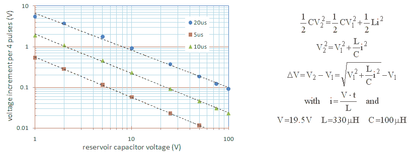
Figure 2.3 Using energy conservation laws it is possible to calculate the incremental output voltage increase per (set of) output pulse(s).
The equations in the Fig. 2.3 rephrase the energy conservation law in mathematical form. In these equations V1 represents the capacitor voltage before the pulse, V2 the capacitor voltage after the pulse, and I the maximum current in the inductor during the pulse. From this the voltage increment can be solved. The voltage increment is obviously in the first place a function of the maximum inductor current at the end of each pulse. This current is as we know directly proportional to the supply voltage and the duration of the pulse, and inversely proportional to the inductance. So the longer the pulse, the higher the current. However, the voltage increment is also dependent on the volage of the capacitor before the pulse. If the capacitor is fully discharged the voltage increment is maximal, and it rapidly decreases when the voltage of the capacitor rises.
Based on the equations it is possible to construct a graph which gives the voltage increment as a function of the capacitor voltage. In Fig. 2.3 this graph is given for three different pulse lengths. In fact the graph in Fig. 2.3 gives the voltage increment per 4 pulses. The reason for this is that the voltage of the capacitor is only measured once every converter 4 pulses due to speed limitations of the AD converter and the software. So the decision to give another set of pulses can only be taken every 4 pulses, so that the minimum voltage increase can also only be due to 4 converter pulses. What we notice from Fig. 2.3 is that for the standard pulse length of 20 us, the voltage increment when the capacitor is completely discharged can be quite large (7-8 V), although it drops quite rapidly when the capacitor becomes a bit charged. In order to increase the voltage resolution for very low output voltage, a bit arbitrarily voltages below 50 V, it is therefore better to reduce the pulse length to 5 us. In that case the output voltage increment (per 4 output pulses) will never be more than 0.5 V.
The high voltage divider
Sometimes very small and subtle changes can have a big impact. This was also the case with the resistive voltage divider network which reduces the 0 – 400 V output voltage of the anode and screen boost converters to a for the AD converter more acceptable 0-5 V. The story starts with the observation that the datasheet of the 16F874 specifies that the maximum impedance of a voltage source connected to any analog input of the controller should not exceed 2 k. This rule of thumb on one hand has to do with the settling time of the sample and hold, and on the other hand with the fact that the current drawn by an analog input is about 500 nA.
The voltage divider I used in the Version 2 uTracer, and that I also want to use for the Version 3, has an impedance a bit less than 6k8 and thus violates this rule somewhat (Fig. 2.4 left). The values for R1 and R2 are in fact a compromise between maximum source impedance to the AD converter and on the other hand current drawn by the voltage divider. Already with R1 + R2 = 560 k the current through the divider at maximum output voltage is in the order of 1 mA. This does not seem much but at 400 V it represents 400 mW resulting in longer charging times and unwanted discharging of the reservoir capacitor during the measurement pulse, so I certainly didn’t want to decrease the resistance values.
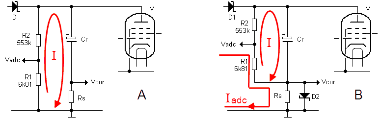
Figure 2.4 Connecting the high voltage divider
At first hand, the left hand drawing in Fig. 2.4 might seem the most obvious and logical way to connect the high voltage divider: between the high voltage node to be measured and ground. The problem with this configuration is that in this way the load current of the voltage divider itself, adds to the current to be measured! In some cases it can even be a substantial part of the measured current, especially so for high voltage / low (screen) current measurements. In fact the current through the voltage divider is one of the major causes of drift and offset in the version 2 uTracer. A very simple but effective way to solve this problem is to connect the voltage divider in the way shown in right hand schematic of Fig. 2.4. In this way the voltage divider current does not flow through the current sense resistor Rs.
This way of connecting the voltage divider is only possible if the voltage drop over Rs is very small. This is certainly the case, normally the only current flowing though Rs is the input current of the analog input of the microcontroller (Iadc) which is in the order of 500 nA. Since Rs typically has a value of 10 – 1000 ohm, the maximum voltage drop caused by this current does not exceed 0.5 mV worst case. The only other case when the voltage drop over Rs can be significant is during a boost converter pulse. This pulse is however very short and even when the AD converter happens to sample the input exactly at this moment, Schottky diode D2 will limit the voltage drop to 0.2 V.
Testing Directly Heated Cathode Tubes
One of the major drawbacks of the version 2 uTracer is that it is impossible to test tubes with a directly heated cathode using the internal supply for the filament. The reason is that the anode current has to follow a path through the NMOS transistor in the filament supply to reach ground.
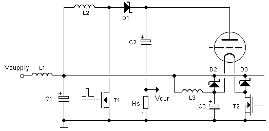
Figure 2.5
| to top of page | back to homepage | to part I |
For some time I have been looking for a suitable box for the uTracer project. As with all my project I don’t like to just buy or order a box from a catalogue or the internet. Part of the fun is to find something old which has been discarded and then try to give it a new life again. For some time I had my eye on an old “automatic printer port switch.” The box was just large enough to hold the electronics, while the top of the box had enough area for a variety of tube sockets. But the box was made out of metal, and metal working is not one of my favorite jobs.
Then a colleague of mine (“Klaus”) moved out of our building to another site on the Campus. People on the move in laboratory environments always offer great opportunities to electronic hobbyists, since people tend to go through their stuff and throw away a lot of interesting things! In the mean time people know me quite well so it happened that Claus came to me with a very pretty plastic box with the question if I had any use for it? Although the front and back plates were missing it was ideal for this project!
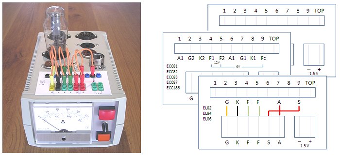
Figure 3.1 A box for the uTracer. Different cards show how to connect the most commonly used tubes. Click here to download the PowerPoint template.
The box is of a particular sturdy German quality, strong enough to hold the tube sockets in it’s top surface. The holes for the sockets were easily made with my good old fretsaw. In Dutch a fretsaw is called a “figuurzaag,” and I have to admit that before writing this
 section I had absolutely no idea what the English word for it was, which just shows that writing these pages is not just a wast of time. My Fretsaw is one of those almost obsolete pieces of equipment that I wouldn’t like to miss although I only use it a few times a year.
To configure the uTracer for a certain tube, I used the very straight forward wiring method using miniature banana plugs. The plugs in the top row (Fig. 3.2) are connected to the pins of the sockets. The plugs in the bottom row are connected to the terminals of the uTracer electronics. Normally such a method to connect the tubes is not recommended because of the inherent safety problem. When disconnected during measurement the wires can carry a lethal voltage. However, in this case when using pulsed measurements the danger is a bit less as compared to the case when the wires would have carried a DC voltage. On top of that there is a big red light flashing on the front panel when a measurement is in progress. Different plug colors were used for different terminals: red for the high voltage anode and screen connections, black for the cathode, yellow of the control grid and green for the filament. There is a double row of bottom plugs so that it is possible to connect more than one tube pin to the same terminal, e.g. in the case when the suppressor grid of a pentode is not internally connected to the cathode. On the right side there are two separate plugs which are connected to a 1.5 V battery. These are used for very fragile battery tubes e.g. from the Dxx96 series.
The position of the plugs in the bottom row was chosen such that for the most commonly used noval tubes a straightforward wiring scheme can be used, e.g. most noval tubes have the filament between pins 4 and 5 so the connections for the filament in the bottom row have been positioned opposite to the plugs for those pins. In PowerPoint a simple template was designed which - when cut out - fits neatly around the plugs. The idea is to design a series of cards for the most commonly used tubes. Just so that I don’t lose the file myself, if can be downloaded here.
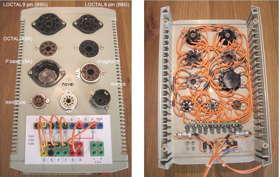
Figure 3.2 The tube sockets and their wiring.
A major concern was the adequate suppression of oscillations in the tube circuit. Martin Forsberg from Sweden kindly pointed me to some of the tricks the designers of AVO used to suppress oscillations in their legendary AVO MARK IV tube tester. First of all they connected the wires connecting the different tube sockets in loops. For example a wire starting from banana plug no. 1 is connected to pin 1 of the first socket, then to pin 1 of the second socket etc, and finally ends again on banana plug 1. Secondly, they made abundant use of EMI suppression beads. These beads are made out of a lossy ferrite and they can be shifted over a wire. They don’t affect the DC resistance but introduce losses at RF frequencies. The aim is to introduce so much losses at RF frequencies that oscillations are prevented. I used 6-hole ferrite beads in series with the wires going to and coming from the banana plugs. I don’t know exactly what type they are, but they must be similar to these from Weurth. At three different places in the tube wiring loops small RF suppression beads from Wuerth (product number 74270015) were shifted over the wires (available from Farnell). I don’t know if all these precautions actually made the difference, but it is a fact that the whole tube socket assembly in combination with the uTracer v2 hardware is oscillation free for all the tubes I have tested so far.
On the front panel of the box there is a big analog meter and selector switch so that it is possible to monitor the voltages of the boost converters and the filament. The push button on the top is an emergency stop button I want to implement in the version 3. It will also contain a lamp which will flash when a high voltage is present at the terminals. When the circuits in the box have their final positions, I will post some more pictures!
| to top of page | back to homepage | to part I |
Until now the firmware boost converter control is only partly interrupt based. A loop in the “main program” continuously measures the output voltages of the boost converters, compares the measured values against their respective set points and then, depending on the outcome of the comparison, sets or resets a control bit which signals the interrupt routine to start or stop with generating boost converter pulses. The interrupt routine itself is called every 100 us, corresponding to a 10 kHz repetition rate. It first checks the control bit of each boost converter. If the control bit is set, the boost converter pulse output is made high (transistor on). The routine then waits for 20 us (the nominal pulse length), and then makes all pulse outputs low (transistors off). After this the routine returns to the main program. Note that in this way the interrupt routine consumes 20% of the cpu time which is mainly spend on waiting (more info).
Working on and with the uTracer2 I realized that this way of controlling the boost converters is far from ideal. The main problem is that when the main program in between measurements needs to spend some time on something else like communications, the boost converters need to be switched off. As a result the output voltages of the converters drops with as one of the main consequences that the negative supply voltage drops, completely upsetting the analog circuitry, sometimes even resulting on a sort of latch-up in the grid-pulse circuit. All in all a good reason to think about how things can be arranged in a more sensible way. Additionally, in the previous section it was concluded that in order to accurately control the output voltage of the anode and screen boost converters in the low-voltage range, the boost converter pulse needs to be reduced to 5 us for voltages below 50 V. So to summarize the requirements for the new boost converter control firmware:
The most straight forward way to implement these functions in the interrupt service routine would be to first measure on each call the output voltage of each of the boost converters, to then decide which output voltage is below the set point, and finally to pulse only those boost converters whose output is too low. Unfortunately life is not that simple. In the datasheet of the 16f874 we find that the AD conversion time consists of two components. The first component is the “A/D Acquisition Time, Tacq,” it is the time needed to charge the sample and hold capacitor after a new AD input channel has been selected. The datasheet specifies the minimum Tacq as 20 us. The AD conversion itself takes a minimum of twelve Tad cycles, with a minimum Tad of 1.6 us resulting in a minimum 10 bit conversion time of 12 * 1.6 = 19.2 us. So in total one AD conversion takes approximately 40 us. Obviously the straight forward method will not work since already the four conversions take up at least 160 us, which is longer than the 100 us interrupt service routine repetition time.
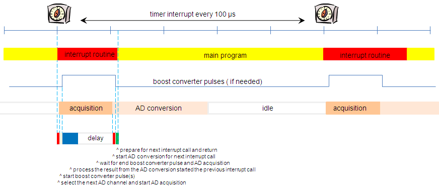
Figure 4.1 Interleaving of the pulse generation and the AD acquisition / conversion in the interrupt service routine.
One solution to overcome this problem is to measure only a single boost converter every interrupt call. This implies that each boost converter is only evaluated every fourth interrupt call, which still amounts to 2500 samples per second! Automatically this means that the boost converter pulses can only be issued in multiples of four. This is also the reason why in Fig. 2.3 I have given the voltage increment of the buffer capacitor per four converter pulses. Actually a single AD conversion sequence aligns surprisingly well with the boost converter timing. Figure 4.1 illustrates how the AD conversion and the evaluation can be interleaved with the boost converter pulse interrupt routine. The top bar represents the time axis and the timer interrupt every 100 us. After an interrupt, the service routine first selects a new analog channel for the evaluation of the next boost converter to be evaluated. Immediately after that the routine starts a new boost converter pulse. This boost converter pulse takes exactly 20 us, the same time needed for the AD acquisition. After these two time critical steps have been taken, the routine has about 20 us of time to evaluate the AD results obtained during the previous interrupt call. During this evaluation the actual boost converter voltage is compared to the set point and based on that a flag is set to indicate that during the next call to the interrupt service routine a boost converter pulse for this particular converter needs to be issued. After about 20 us the boost converter pulse(s) are ended and the actual AD conversion is started. After this the routine exits and execution of the main program is resumed. The AD conversion itself is therefore performed in parallel with the execution of the main program. The timing parameters for the AD conversion need to be set such that the AD conversion is ready before the next interrupt call.
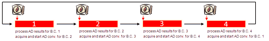
Figure 4.2 Every call to the interrupt service routine the boost converters are pulsed (if needed) but only one AD conversion is started and evaluated.
The whole process is also illustrated in Fig. 4.2 for the case when there are four boost converters. Every time when the interrupt service routine is called, the results from the previous AD conversion are digested while an AD conversion for the next call is started. After four calls the loop starts all over again. To do all this in just one routine would require quite some overhead (speed) in the form of “IF call=1 THEN … ELSEIF call=2 THEN … ELSIF call=3 THEN … ELSE …” statements. To avoid this, four different routines are used, each one only having a single branch in the form of “IF call=1 THEN this_routine” statement at the beginning.
Mask bytes
Actually the whole situation is a bit more complex. We not only need to generate boost converter pulses of 20 us, but in some cases also pulses of only 5 us. We have seen that for accurate regulation of anode and screen voltages below say 50 V, a boost converter pulse of only 5 us gives a much better control of the output voltage. One way or the other this has to be implemented in the interrupt service routine.
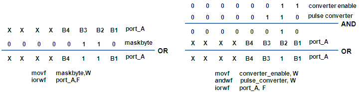
Figure 4.3 The use of “mask-bytes” to switch the boost converters on.
The biggest problem here is speed: in the interrupt service routine there is not enough time to do extensive branching and or computation, so the algorithm which has to decide if a pulse needs to be 20 us or 5 us has to be implemented as efficiently as possible. The good news is that the information about the pulse length is already known at the beginning of a measurement cycle.
The implementation I have used here uses “mask bytes.” To explain how it works we assume that the boost converters 1 to 4 are connected to PORT_A,0 to PORT_A,3 (Fig. 4.3 left). So when PORT_A,0 is made high, boost converter 1 is pulsed. Now, the information which boost converter needs to be pulse is stored in the “mask byte” (Fig. 4.3 left). By now simple “OR-ing” the mask byte with PORT_A, and storing the result in PORT_A, the boost converters whose corresponding bit in the mask byte was set high is pulsed. The bits in the mask byte in turn are set or reset by the AD conversion part of the interrupt service routine itself.
In reality it is even a bit more complex because also the main routine must be able to enable or disable each individual converter. That information is stored in byte “converter_enable” (Fig. 4.3 right). The results from the AD conversion evaluation are stored in byte “pulse_converter”. A logical AND between the bytes results in a “1” for the converter that needs to be pulsed, so “OR-ing” this result with PORT_A will activate the appropriate converters. In this way up to 8 converters can be controlled simultaneously using only three instructions (= 600 ns).
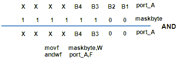
Figure 4.4 The use of “mask bytes” to switch the boost converters off.
A similar trick is used to decide which converter needs to be switched off after 5 us. Again a mask byte is used which is programmed by the main program already before the start of a measurement cycle. When a particular converter needs to be switched off after 5 us, the corresponding bit in the mask byte is made 0 while all the other bits are “1” (Fig. 4.4). By simple “AND-ing” the mask byte with PORT_A and storing the result in PORT_A again, the corresponding converter pulses are terminated. The whole procedure takes only 2 instructions (= 400 ns). After in total 20 us all converter pulses are terminated by “AND-ing” zeros for all the converters into PORT_A.
Confused? So am I, but it is all very efficient and fast!
| to top of page | back to homepage | to part I |
People who have followed this uTracer project from the start, will no doubt recall that in version 1 of the uTracer the tube was pulse by switching the anode and screen voltages on with a “high side” transistor switch. This concept caused a lot of problems, mainly because it is very difficult to find an affordable high voltage pMOS transistor and because it was difficult to implement a reliable over-current protection. Additionally, the direct coupling between the high voltage and the low voltage controller electronics posed the thread that in case of a mal function the controller electronics can easily be destroyed, as it did in one occasion. Basically these are the reasons why in the version 3 uTracer the switching function is done by the tube itself which is a very rugged switch which can be easily overloaded. However, this concept also has several drawbacks:
The high voltage switch (again)
I spend quite a long time thinking about a circuit topology which uses an nMOS transistor to switch the anode and screen voltages. As expected that is not so easy. The only circuit topology that I came up with is the standard solution which uses a pulse-transformer. However, the pulse length is on the long side for a pulse transformer, resulting in high inductance values so that I probably would end up using a custom made transformer, something which would make me very unpopular with my readers.
So almost unavoidably we are stuck with either a pMOS or a pnp transistor. I made a search for a good high voltage pMOS. It is really surprising how few discrete pMOS devices with a breakdown above 300 V are on the market. One of the few devices I could find is the STD3PK50Z from ST, and even this device is only available for evaluation purpose only. The reason for this is surprising and something I need to dive into one of these days. The situation is a bit better for pnp devices, although also here the choice is rather limited. One of the most common medium power pnp devices available is the MJE350 with a BVceo of 300 V. This transistor is offered at prices less than 1 euro by e.g. Farnell. A similar transistor with a BVceo of 350 V is the BF588 of NXP. Unfortunately this transistor is less commonly available.

Figure 5.1 BVceo measurement of an MJE250 compared to a BF588
Figure 5.1 shows a measurement of the BVceo (openbase collector to emitter breakdown voltage) for both an MJE350 (left) as well as an BF588 (right). The vertical axis shows the collector current while the collector-emitter voltage is sweeped and displayed on the horizontal axis. The bottom curve is for Ib = 0 while for every next curve the base current is incremented with 5 uA. For the MJE350 we find a BVceo of ca. 420 V and for the BF588 ca. 500 V. Read more about breakdown voltages in diodes and transistors Here. Although the BF588 has a somewhat higher BVceo and also a higher HFe, I will try to use the MJE350 because it is so commonly available and very cheap. Considering the BVceo of 420 V it will be best to limit the test voltages to 350 V.
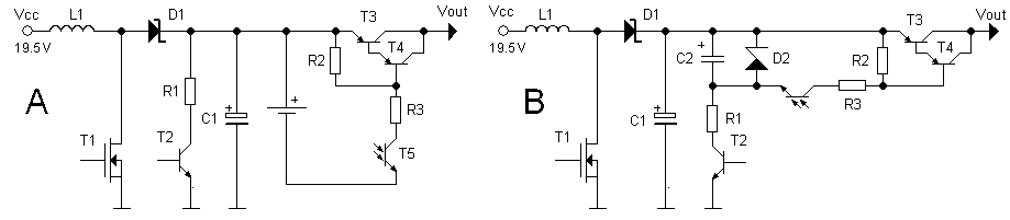
Figure 5.2 Principle of the “opto-coupled” high voltage switch (left), and the circuit implementation of the floating battery with a capacitor (right)
Figure 5.2A shows the concept of a “high-side” pnp switch which is controlled by an opto-coupler. T1, D1, C1 and L1 represent the high voltage boost converter. Transistor T2 and R1 form the discharge circuit. Recall that when the new set-point value for the boost converter is lower than the current output voltage, the discharge circuit first discharges the buffer capacitor C1 to a value below the set-point before it is charged again to the new set-point. The pnp switch has again been implemented as a Darlington to be able to completely pull T3 deep into saturation with a minimum of base current. In this conceptual diagram the base current for T4 is provided by a separate battery which is floating with respect to ground. R3 and R2 are selected such that when phototransistor T5 starts to conduct, Darlington T3/T4 will be driven into saturation.
So far so good, but how to implement a floating battery? I have to admit that it took me quite some thinking to figure out an elegant solution. The trick I came up with in the end is explained in Fig. 5.2B. As can be seen the battery is replaced by the small capacitor C2. The capacitor holds enough charge to be able to drive the pnp Darlington for 1 ms. But how to ensure that the capacitor is always charged? A simple resistor wouldn’t work because that would charge the capacitor to the maximum voltage which can be as high as 350 V, way too high for the opto-coupler. A simple zener diode of say 10 V limits the voltage, but causes a leackage current which would unnecessary load the boost converter. The simple trick was to replace the resistor with the discharge circuit consisting of T2 and R1. The value of R1 is relatively low (ca. 10k) so that C2 is very quicky charged. The beauty of the thing is that in this way the discharge circuit serves two functions: to discharge C1 before a charge cycle, and at the same time to quickly charge C2.
A few back of the envelope calculations confirm the validity of the concept. Suppose we take for C1 a capacitor of 1 uF. We don’t want to use an electrolytic capacitor because they possibly might have a too high self-discharge rate. With a zener diode of 10V, the longest charging time occurs when C1 is at its minimum voltage of Vcc = 20 V. In this case the minimum charging current is (20-10)/10k = 1 mA. So to charge C2 to 10 V in the worst case requires: (V*C)/I = (10*1E-6)/1E-3 = 0.01 s. Suppose on the other hand that a base current of 2 mA is used to drive the pnp Darlington. The drop in voltage of C2 in that case amounts to: (I*t)/C = (2E-3*1E-3)/1E-6 = 2 V, which is of course very acceptable. In short the idea might very well work!
The current amplifier & over current protection
In the version 2 concept the current range switching was performed by switching between two different series resistors using a mechanical relay. These relays are not only relatively large, but also pose a reliability issue since the current can be quite large, and additionally they can introduce noise. With the current sense resistor in the concept 2 version on one side firmly connected to ground, the main source for drift and offset has been removed. It now becomes feasible to use an active amplifier to switch between the different current ranges. Experimenting with the version 2 uTracer I found that the two measurement ranges 0-20 mA and 0-200mA were a bit too limited at the low current side. It would be very nice if a 0-2 mA range could be added.
A great deal of time was spent in reviewing different circuit topographies to achieve this. The first idea was (as always) to use as much as possible standard of-the-shelf components. However, the three measurement ranges would at least require three low-offset OpAmps and some analog MUX since the number of analog inputs on the microcontroller is limited. Standard OpAmps require a -/+ 15 V power supply so that quite some diodes and resistors are needed to protect the 0-5 V ADC input of the microcontroller. All in all not a very elegant conclusion. After looking at the pros and cons of the different concepts I came to the conclusion that really the best and most elegant solution was to use a modern Programmable Gain Controlled Amplifier (PGA). The PGA113 is such a device made by Texas Instruments. It uses a single 5 V power supply with 0-5 V input range. It is controlled by a simple digital serial SPI interface which allows for the selection of one of the following gains: 1,2,5,10,20,50,100,200 (Scope gains)! On top of that it has extensive features for drift and off-set calibration. Even better is the price which is only 3 euro, even at Farnell., while the component is also available for free sampling from TI directly! Really its only drawback is that it only comes in one of these impossible 10 pin super-small outline packages (SSOP). The IC is really impossible small, but fortunately I have a few adapter PCBs to bring the pinning to standard DIL dimensions, but I am not looking forward to the job of placing it on the PCB.
Figure 5.3 Schematic circuit of the current sense amplifier and the over-current protection.
Figure 5.3 shows the principle of the current sense amplifier and over-current protection as I have it now planned. The current is measured over resistor R1. The value of R1 is a bit of a compromise. On one hand the value should be so low that even at the maximum current range the voltage drop over it is small compared to the anode voltage. On the other hand making R1 too small will make it impossible to accurately measure the low current range. With respect to the first requirement it can be argued that this argument is less serious since it is always possible to correct for the voltage drop over the current sense resistor since both the value of the resistor and the current are known. So for an AD converter with an input voltage range of 0-5 V, R1 is selected such that for the maximum current of 200 mA the input voltage is about 4 V, so R1 = 20 ohm.
Due to the direction of the current flow during the measurement pulse, the voltage drop over R1 is negative with respect to ground. OpAmp A1 inverts this voltage drop with an amplification of A=-1. Diodes D2 and D3 protect the OpAmp for any accidental over-voltage condition. The diodes D4 and D5 in combination with the current limiting resistor R4 clip the output voltage of the OpAmp to the analog power supply range to protect the PGA. The circuit around the PGA is very simple. The gain is controlled by a two wire serial SPI bus which is directly driven by the microcontroller. The output of the PGA is directly connected to one of the analog inputs of the PIC. Since the output voltage of the PGA can only be within the analog supply voltage range (0-5V) no input protection for the PIC is needed here.
The over-current protection is implemented in a very simple but elegant way. There are two ways to implement an over-current protection. The first way is to limit the current to a certain maximum value. Such an over-current protection circuit doesn’t make much sense here. Suppose that the buffer capacitor is charged to 400 V and that the current in case of a short circuit is limited to 200 mA, even in that case the momentary dissipation in the high voltage switch is 80 W. This is about 4 times the maximum specified dissipation for an MJE350. Although the measurement pulse is very short, it can very well be that this is ok, but it is on the edge of what is safe. Another over-current protection method is to immediately shut down the high voltage switch as soon as an over-current condition is detected. The measurement will be out of range and invalid anyway! My first idea was to implement such a circuit using a discrete comparator and some flip-flops. I then realized (de Wedert, Valkenswaard) that the PIC has two comparators on board which had not been used so far. Even better, the reference to these comparators is to some extend programmable so that it becomes possible to implement a programmable over-current protection. To make the response of the controller very fast, the over-current handling has to be interrupt driven, but that is no problem since the (interrupt based) control of the boost converters is suspended during the measurement pulse anyway! In this way it should be possible to respond to an over-current situation in less than a few micro-seconds, which will be small in comparison to the response time of the opto-coupler. All in all I was very pleased with this elegant solution, if I say so myself.
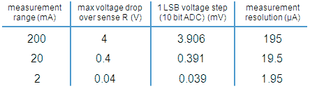
Table 5.1 Some system specifications based on a current sense resistor of 20 ohm.
With the gain of the PGA at 100X, the lowest measurement range is 0-2 mA. Assuming a current sense resistor of 20 ohm, this corresponds to a maximum voltage drop of 40 mV (Table 5.1). For a 10-bit ADC this results in a voltage increment per LSB of slightly less than 40 uV! This implies that the total offset of the measurement system should also be less than 40 uV, quite a challenge! The main sources for offset errors are the inverting OpAmp A1 and the PGA. For the OpAmp I am planning to use a cheap OP177. This precision OpAmp has a typical offset of 20 uV and a maximum offset of 60 uV. The PGA 113 has a typical offset of 25 uV and a maximum offset of 100 uV. So typically the offset error should be about 1 LSB, but it can add up to about 6 LSB. The OP177 has the possibility for an external offset compensation and I just will have to see in how far it is possible to compensate for the total system offset.
What is missing in this section are of course measurements and experiments. Well, the weather has been just too good and besides that my “lab” was in such a terrible state that I really had no appetite. But the mess has been cleaned up (to some extends) and the first experiments have been carried out!

| to top of page | back to homepage | to part I |
I have to admit that I had to over win quite an emotional barrier to start working on the high voltage switch again. I still vividly remember the experiments with the high voltage switch for the version 1 uTracer, which in the end turned out to be such a disappointment that the whole concept of high voltage switches was abandoned in favor of the version 2 concept which uses the tube itself as the current switch. However, after having convinced myself that the new concept as described in the previous section should represent a huge improvement over the previous high voltage switch I set to work.
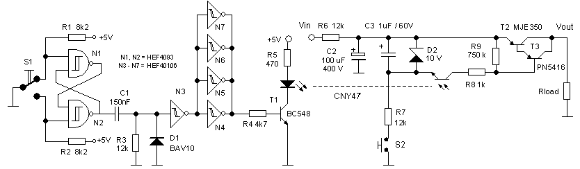
Figure 6.1 Basic test circuit used to test the new-concept high voltage switch.
Figure 6.1 depicts the basic test circuit that was used in this new series of high voltage switch experiments. Regular readers of these pages will undoubtedly recognize the pulse circuit from the original test circuit. It is obvious that the pulse circuit on the left is completely galvanicly isolated from the high voltage switch. Pressing of S1 generates a pulse of approximately 1 ms. The high voltage buffer capacitor C2 is charged via a resistor of 12 k to limit the current during an accidental short circuit. The discharge transistor is emulated by switch S2. Shortly pressing S2 will charge capacitor C3 to 10V. In the experiments the configuration around the high voltage transistors T2 and T3 was varied to optimize the properties of the switch.
Limiting the current
The current limit provision consists of two mechanisms. The first mechanism was discussed in the previous section. It consists of a sense circuit which measures the current and in case of an over-current situation completely switches off the current. This part of the over current protection is completely implemented using the comparators and the interrupt mechanism of the micro-controller. However, this protection takes some time to react. First of all because the microcontroller needs time to execute the proper interrupt code, secondly because the opto coupler needs some time to completely switch off. In total the latency can add up to 20-30 us! To limit the current during this time it is necessary to implement some kind of fast current limiting mechanism.
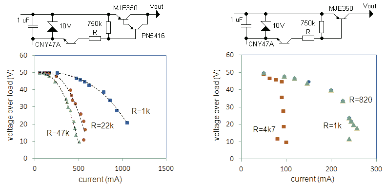
Table 6.4 Experiment to investigate if it is possible to limit the output current by limiting the base current of the switching transistor.
The standard solution to realize this is to include a small series resistor in the emitter of the Darlington and an additional transistor which “pulls away” the base current of the Darlington when he voltage drop over the resistor becomes about 1.0 V. However, before adding another transistor I thought it was perhaps possible to do it in a more clever way. The idea was to make use of the fact that for high currents the current gain of a bipolar transistor collapses due to what we call high-injection effects. So suppose that due to a short circuit the collector current increases to values in this high injection regime. As a result the base current will more than proportionally increase due to the hFE drop-off. By simply selecting the base resistance to such a value that it can no longer supply this current, it should be possible to limit the base- and stabilize the collector current.
To test this idea the circuit of Fig. 6.1 was used with a decade resistor as load. The output voltage pulse was recorded with a memory scope and from the pulse height and the resistance value the current was calculated. The results for three base resistance values are recorded in the left graph in Fig. 6.2. We clearly see that the effect as predicted can be clearly observed. For increasing base resistance the maximum current decreases. However, it appeared that in order to reduce the maximum current to a value of ca. 250 mA, such a high base resistance is needed that for currents well below 200 mA the saturation voltage of the Darlington pair increases to an unacceptable value. Just to satisfy my own curiosity, I also tried the same idea with only the MJE350 (Fig. 6.2 Right). Here the effect was even worse. So I am afraid that reliable current limiting can only be obtained at the expense of an additional transistor.
Response time for power shut-down
As discussed previously the microcontroller shuts-down the high voltage switch when an over-current condition is detected. Obviously it is important to minimize the response time here as much as possible. The response time consists of three components: the slew-rate of the inverting OpAmp which inverts the negative voltage drop over the current sense resistor, the response time of the microcontroller, and the response time of the high-voltage switch itself. As far as the OpAmp is concerned, that’s basically just a matter a selecting a type with a very low offset and a reasonable slew-rate. The OP27E for example has an offset of 10 uV (typically) combined with a slew-rate of 3 V/us, resulting in a response time of only a few microseconds. As stated before the response time of the microcontroller is also in the order of 1 to 2 microseconds, which probably leaves the high voltage switch itself as largest contributor to the total delay.
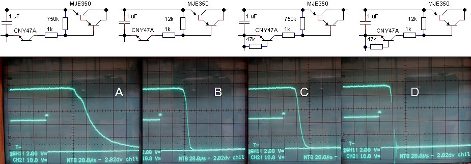
Table 6.3 The speed of the high-voltage switch can be significantly improved by adding an additional current path to the emitter-base junctions of the transistors.
Figure 6.3A depicts on the upper trace the output voltage of the high voltage switch as measured over a 200 ohm resistor. The input voltage was set at the still relatively save value of 50 V so that the current amounted to 50/200 = 250 mA. The lower trace depicts the pulse signal driving the switch (outputs inverters N4-N7). The total pulse length was 1 ms, and the memory scope was set to trigger on the falling edge of the input pulse. Observe that the output voltage of the switch remains high for ca. 40 us and then decays with a tail of about 100 us.
The delays are caused by the fact that all the transistors in the circuit are driven deep into saturation. This means that both the emitter-base and the collector-base junctions are forward biased and are injecting large amounts of minority carriers in the base. For the transistor to switch off, these carriers first have to recombine. The “problem” is that today the quality of the transistors is just too good. By perfecting transistor technology, the recombination rate in the base has been made very small. On one hand this results in a nicely linear hFE, but on the other hand it increases switching speed. By providing an additional current path to the base, it is however possible to improve matters a bit. In Fig. 6.3B the emitter-base resistance of the Darlington was lowered to 12k. This almost completely removes the switching tail of the curve. Alternatively in Fig. 6.3C a resistor was added between the emitter-base of the photo-transistor of the opto-coupler. This simple measure decreases the high time of the output voltage from 40 to 20 us. Finally, in Fig. 6.3D both measures were implemented resulting in a nice sharp switch-off ,and a delay of only 20 us. Good enough for the time being.
The saturation voltage
The saturation voltage of a single bipolar transistor can easily be as low as 100–200 mV. Unfortunately that is different for a Darlington. As soon as the collector-base voltage of the power transistor becomes zero (the definition of the point of saturation) the collector-base junction of the driver transistor becomes forward biased thereby pulling away base current of the power transistor. The saturation voltage of the darlinton pair as a whole can therefore never be lower than approximately one build-in junction voltage (0.6-0.8 V).
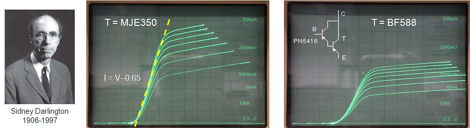
Figure 6.4 Ic-Vce curves of a Darlington constructed with an MJE350 (left) and a BF588 (right).
For more information on Sidney Darlington (click here).
Figure 6.4 shows the Ic-Vce curves of a Darlington constructed with an MJE350 (left) and a BF588 (right). Note that the MJE350 Darlington, despite the significantly lower hFE as compared to the BF588, not only requires a substantially less base current for the same collector current, but also has a lower saturation voltage. The reason for both observations is presumably the fact that the high injection point for MJE350 starts at a somewhat higher current.
The relatively high saturation voltage is not really ideal. In a perfect world we would have preferred a switch with a zero voltage drop. Fortunately the voltage drop is limited to a value less than 1 V, and on top of that the voltage drop is a simple almost linear function of the current. The dashed line in Fig. 6.4A approximates the saturation voltage as a function of current and is described by I = V-0.65. So in other words the saturation voltage is given by V = I+0.65. With this simple formula the GUI software can easily compensate for the voltage drop over the transistor, as well as of course for the voltage drop over the current sense resistor and the current limit resistor.
Short-circuit proof
From the previous experiments it became clear that limiting the output current just by limiting the base current was not feasible. So a “real” current limiting circuit was implemented in exactly the same way as for the version 1 uTracer. Figure 6.5 depicts the circuit diagram of the high-voltage switch including the current limiting circuit and the current sense resistor and amplifier. The current limit circuit consists of R10 and T4. When the voltage drop across R10 reaches ca. 1 V transistor T4 is switched on thereby limiting the current through the Darlington pair. With a value of 2.7 ohm the current is limited to ca. 240 mA.
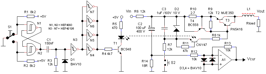
Figure 6.5 Test circuit for the high-voltage switch including the current-limiter circuit and the current sense resistor and “amplifier”.
With the current limit circuit implemented short circuit tests were performed. My initial hope was that when the current is limited, an MJE350 would survive a short circuit pulse at 350 V. With a maximum current of 250 mA the instantaneous power dissipation then amounts to 350*0.24 = 84 W. The absolute maximum dissipation for an MJE350 at 25C is specified as 25 W, but I had the hope that under pulsed conditions the dissipation could be somewhat higher. Alas, this was not the case.
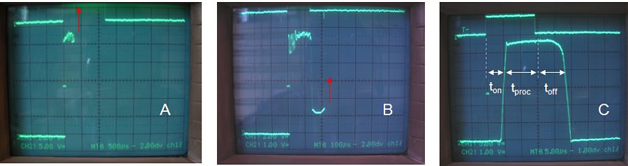
Figure 6.6 A (200 V) and B (300 V) show the breakdown of the MJE350 under short circuit conditions (see text). C shows that for short pulses the switch holds up to 350 V.
Figure 6.6A depicts a measurement where the high voltage switch was pulsed for the nominal time of 1 ms at a voltage of 200 V with the output shorted. The upper trace is the pulse signal itself which is used to trigger the scope. Observe that the pulse length is about 1.2 ms. At first the switch holds and limits the current to ca. 240 mA. Then after about 300 us it breaks down (red arrow) resulting in a shorted MJE350. None of the other components were damaged. This demonstrates that the over-current switch-off loop that I want to implement using the controller is no luxury, but an absolute necessity! The problem is that this protection loop requires some time to respond. To see how far things could be stretched, the pulse length was reduced to 120 us by reducing C1 to 8.6 nF (3x 2n2). The switch again failed, but now at 300 V. Figure 6.6B shows the actual measurement. Observe that initially everything works fine and that the Darlington is switched off, then just before the Darlington is fully switched off the MJE350 breaks down.
Again the pulse length was reduced, this time to 15 us (Figure 6.6C). The delays “t_on” and “t_off” are associated with the response time of the opto-coupler, the Darlington and the inverting OpAmp. The delay “t_proc” simulates the response time of the microcontroller. So in this case we suppose that the microcontroller needs about 10 us. In reality the microcontroller will respond much faster so that this represents a worse case situation. The switch now holds for a full short circuit condition for voltages up to 350 V, possibly higher, but this was not tested.
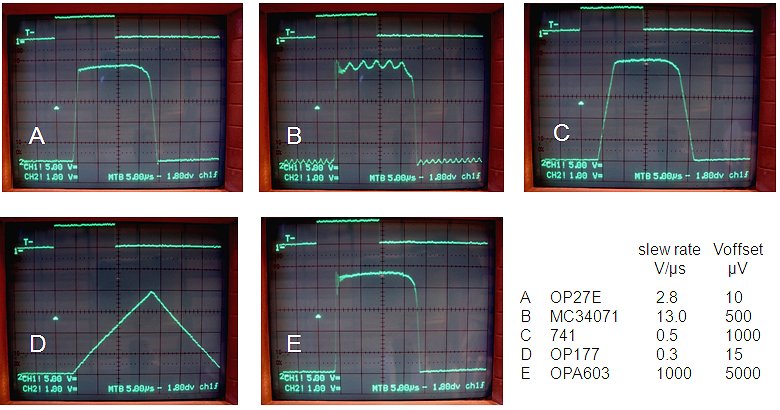
Figure 6.7 The measurement of Fig. 6.5C repeated with different OpAmps for the current sense amplifier.
The delay caused by the inverting OpAmp is one of the more important components in the response time of the microcontroller control loop. For the selection of the OpAmp it is thus important that it has a low-offset voltage (order of 25 uV) and a high slew-rate. Just to see the difference between different OpAmps, I repeated the measurement of Fig. 6.5C with 5 different OpAmps that I happened to have “on stock.” Note that the OP177 I had originally in mind would have been way too slow. An OP27E is a much better choice with respect to speed for the same offset voltage.
Testing with real tubes
Finally the high voltage switch was tested on two real tubes, an EZ81 double diode and an EL84 power pentode. Basically the circuit of Fig. 6.5 was used, but Rload was replaced by the anode of the tube, while the cathode was grounded. The filament, and the grid in case of the EL84 were supplied from an external power supplies. The current was measured by measuring the voltage drop over the 18 ohm current sense resistor using the memory scope.
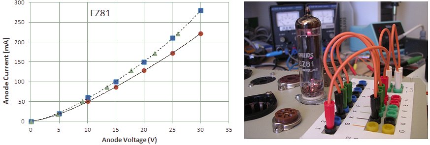
Figure 6.8 Anode current versus Anode voltage for an EZ81 double-diode.
Figure 6.8 shows a measurement of one of the diodes in the EZ81. The circles and the continuous line show the anode current versus the anode voltage as set by the “high-voltage” input of the test circuit. The squares and the dashed line give the anode current versus anode voltage from the graphs in the original Philips datasheet. As seen there is quite an offset between the curves. Especially for higher current part this offset is caused by the voltage drop over the current sense resistor which can amount to up to 4 V. Since the exact current, as well as the value of the sense resistor are known, it is straightforward to compensate for this voltage drop. In this way it is not possible to exactly set the anode and screen voltages (there will always be some deviation dependent on the current) but at least it is possible to calculate the exact anode-cathode voltage for the graphs. The measured data compensated for the voltage drop over the sense resistor is represented by the triangles. Amazingly enough the measured data now more or less overlays the graphs from the datasheet.
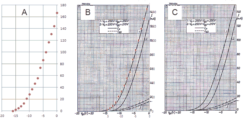
Figure 6.9 Anode current versus grid bias for an EL84 (Vanode = 250 V, Vscreen = 250 V).
Figure 6.9 shows an anode current versus grid bias measurement for an EL84 power pentode. The curve seems to be build up from three different parts, each part corresponding a different vertical scale setting of the scope. The left graph depicts the measured data as is, the right graph is taken from the original Philips datasheet. In the center graph the measured data graph was scaled so that the axes overlay with the datasheet graph. Again the measured data almost coincides with the graph in the datasheet. It is absolutely amazing that these tubes after being switched on again after 60 years exactly reproduce their original behaviour!
| to top of page | back to homepage | to part I |
The grid bias generator has to convert a 0 - 100% Pulse-Width Modulated (PWM) 0 - 5 V square wave from the microcontroller into a 0 to -50V voltage for the control grid of the tube. It consists of three parts:
Just as in the case of the grid-bias circuit for the version 2 uTracer, it took quite some puzzling to come to a circuit which does the job, and at the same time is simple and does not require the use of exotic components. The requirements of this grid bias circuit compared to the version 2 circuit differ in the sense that in this case the cathode of the “tube-under-test” is connected to the (unregulated) 19.5 V power supply, rather than to ground (see Section 2). So also the negative grid bias needs to be generated with reference to the 19.5 V power supply voltage. Since a new circuit needed to be designed anyway, I thought it was a good moment to review the complete circuit and make some improvements where needed:
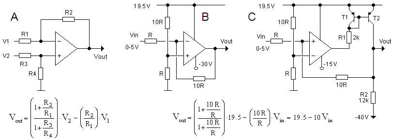
Figure 7.1 A) basic differential amplifier circuit, B) principle of the grid bias circuit using an ideal OpAmp, C) principle of the grid bias circuit using a realistic OpAmp and a high voltage output stage.
The core of the new grid bias circuit is the well known “substraction” or differential amplifier circuit (Fig. 7.1A). Usually in the formulas given for this circuit it is assumed that R1 = R3 and that R2 = R4 resulting in the well known equation Vout = (R2/R1)*(V2-V1). However, in the more general case R1, R2 R3 and R4 all have different values. In that case the
 relation between the output voltage and the input voltages is given by the equation given in Fig. 7.1A. We now tie input V2 to the 19.5 supply voltage (the cathode potential) and alternatively assume R2 = R3 = 10*R1 = 10*R4 (Fig. 7.1B). The formula for the output voltage now reduces to the equation given in Fig. 7.1 B. We define the grid bias as the voltage difference between the cathode (positive supply voltage) and the grid itself. In that case for zero input voltage the output voltage of the OpAmp is 19.5 V, or in other words: zero grid bias. When the input voltage is increased to 5 V, the grid bias linearly increases to -50 V, exactly what we need.
The circuit in Fig. 7.1B assumes a rather unrealistic OpAmp. In the first place because of the enormous supply voltage of V+ = 19.5 to V- = -30V. In the second place because the circuit assumes that the output voltage of the OpAmp can swing from the positive supply rail down to the negative supply rail. For most OpAmps, especially the ones with a somewhat large supply voltage range, this is not the case. So in the circuit of Fig. 7.1C a special output stage is added which converts the limited output swing of the OpAmp to a much larger output swing which can even go below the negative supply voltage of the OpAmp.
The special output stage basically consists of a pnp current mirror tied to the 19.5 V supply voltage rail. In principle the current flowing though T1 is mirrored through T2. The current through T1 is determined by the output voltage of the OpAmp and the value of R1. When the output of the Opamp is high, the current through R1 is low, so also the current through T2 is low, so the output voltage is low. Alternatively when the output voltage of the OpAmp is low, the output voltage is high. With R2 > R1 the output voltage swing of the circuit can be larger than the output voltage swing of the OpAmp. Since the output voltage of the circuit is fed back to the input of the differential amplifier circuit, the exact relation between the input and output voltage is completely determined by the resistors in the OpAmp circuit, just as in Fig. 7.1B. Note that since the output stage inverts, the positive and negative inputs of the OpAmp have been exchanged in Fig. 7.1C.
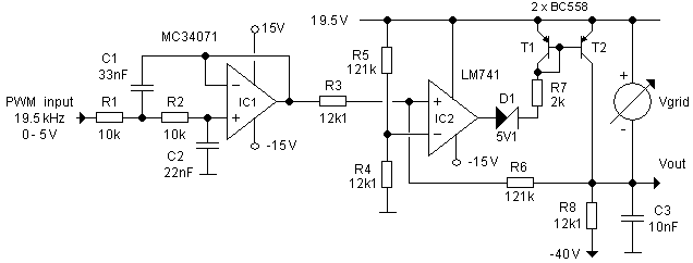
Figure 7.2 Test circuit used to evaluate the new grid bias circuit.
Figure 7.2 shows the circuit that was used to test the new grid bias circuit including the low pass filter that is used to convert the PWM signal to an analog signal. The filter was not used in all the measurements but instead for the graphs shown in Fig. 7.3 only a variable DC voltage was applied to R3. The left graph in Fig. 7.3 and the small insert show the grid bias – so the voltage difference between the cathode (the 19.5 supply) and the output of the circuit (the grid) – as a function of the input voltage. Note that there is a nearly perfect 10:1 relation between the input voltage and the output voltage. Below a grid bias of 1 V the output transistor T2 is driven into saturation. This causes a small deviation from the ideal 10:1 behavior as shown by the insert. The right graph in Fig. 7.3 shows for the same input voltage range the output voltage of the OpAmp.
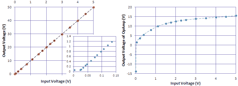
Figure 7.3 Left: grid bias versus input voltage (insert showing detail for very low grid bias values), Right: output voltage of the OpAmp versus input voltage for the test circuit depicted in Fig. 7.2.
With respect to the final circuit diagram shown in Fig. 7.2 a few points need to be mentioned (before I forget them):
About Grid Current
A few times the grid current was mentioned in this section, but actually in normal operation – with the grid at a negative potential – the grid current is usually very small. It originates from electrons being emitted from the cathode which “accidentally” are collected by the grid (Fig. 7.4). Note that the direction of the current is pointed “into” the grid. The value of the grid current is very small. Only for very low grid bias values it has a value of any significance. For negative grid biases the grid current very quickly reduces to practically zero. Also for increasing anode voltage the grid current decreases. The maximum grid current is therefore measured zero grid-cathode bias and zero anode voltage.
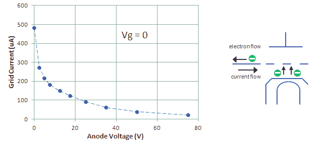
Figure 7.4 Control grid current at zero grid bias as a function of anode voltage voltage for an EF80.
The value of the grid current strongly depends on the type of tube. Obviously the smaller the distance of the grid to the cathode, and the smaller the distance between the turns of the grid, the higher the grid current. As an illustration the grid current was measured for several tubes at zero anode and grid bias: EL84 Ig=-41 uA, EF80 Ig=-470 uA and ECC83 Ig=-200 uA. Figure 7.4 (left) shows the decrease of grid current for increasing anode voltage for the EF80.
| to top of page | back to homepage | to part I |
In an instrument like the uTracer, which handles voltages of several hundreds of Volts at currents of several hundreds of mA, it is obvious that an error or malfunction can easily result in the destruction of (a part of) the circuit, especially so since the uTracer is build up from sensitive semiconductors. I vividly recall how a malfunctioning high voltage switch in the version 1 uTracer resulted in a complete destruction of all the semiconductors in the circuit! Although I was under the impression that I had pretty well covered the issue of robustness in the current version 3, a remark made by one of the faithful readers of these pages, Martin Forsberg, caused me to re-think the whole robustness issue, and to make several important modifications.
Let’s first start by analyzing the potential problems:
Figure 8.1 shows in a simplified circuit diagram the most important components of the safety features that have now been incorporated into the present uTracer V3 to improve its robustness. In block 1 we find the boost converter itself. Although this is not a safety feature in itself, the fact that the amount of energy stored in the capacitor is limited obviously greatly helps. But nevertheless, at a maximum voltage of 350 V, the energy stored in the 100 uF capacitor is 0.5*C*V^2 = 6.1 J. Although this is just enough energy to raise the temperature of 1 cc water 1.5 degree, it can easily destroy a whole board of semiconductors! Block 2 in Fig. 8.1 is the high voltage switch. In this block three safety features have been implemented which have already been discussed in one of the previous sections. In the first place a current limiter limits the maximum anode / screen current to 250 mA. In the second place when an over current is detected, the microcontroller shuts-off the high voltage switch in ca. 50 us. Finally, the complete high voltage switch is galvanically isolated from the rest of the circuit by means of an opto-coupler. This isolates the micro-controller from the high voltage switch in case of a malfunction or breakdown of the high voltage switch itself.
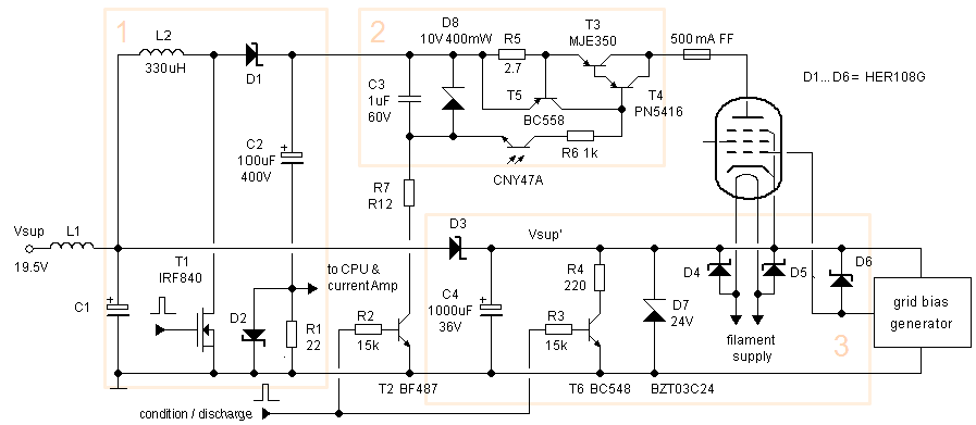
Figure 8.1 Overview of the safety features included in the version 3 uTracer.
Block 3 in Fig. 8.1 needs some explaining. In section 2 of this page it was explained that by referencing the cathode to the supply voltage rather than to ground it becomes possible to apply anode voltages down to zero. We have already seen that it is very simple to protect the filament driver circuit against high voltages by clamping the filament terminals to the cathode with two diodes (D4,D5), or in other words to the supply rail. Similarly the grid bias circuit can also be protected with a simple clamp diode (D6). The consequence is however that both during normal operation, as well as when the protection diodes are activated, the current is dumped into the supply rail rather than to ground! Potentially this can “lift” the supply rail and in that way cause damage to the rest of the circuit or even the power supply.
In the further discussion of the consequences we consider two cases. In the first case the high voltage switch and current limiting circuit function as they should. This means that the maximum current is 250 mA
 for a pulse duration of 1 ms. Under these normal circumstances it should be sufficient to simply decouple the power supply with a large capacitor of say 1000 uF. A pulse of 250 mA for 1 ms in a 1000 uF capacitor will result in a voltage increase of only (0.25*0.001)/0.001 = 0.25 V. However, let’s now assume that for one reason or the other the high voltage switch fails, so that the complete charge of the boost converter reservoir capacitor is dumped in the power supply rail. If no special precautions are taken, this may result in very high voltages on the supply rail indeed!
To be absolutely sure that even under these unusual circumstances no damage is done to the rest of the circuit, that part of the supply rail which is connected to the cathode and the protection diodes is isolated from the main supply rail by means of diode D3. The voltage on the isolated part is limited to 24 V by means of zener diode D7. This special surge protection diode is especially designed to handle short pulses of high currents. When D7 starts conducting, the current will very quickly increase, “blowing” a fast acting 500 mA fuse to prevent further damage to the capacitor.
The last thing that needs explaining is the function of transistor T6. As explained, during normal operation every measurement pulse will inject current into the supply rail. Since now the supply rail has been isolated by means of D3, these current pulses may cause a charging of C4. Although some of this charge will leak away through the grid bias circuit, T6 was added to be sure that C4 is reset before every measurement pulse. The same 10 ms pulse which drives the transistor that charges C3 is used for this purpose. A simple bleeder resistor could also have been used, but since C4 is quite large it is difficult to select a resistor value so that the resultant time constant is small enough without causing too much dissipation.
| to top of page | back to homepage | to part I |
The uTracer V2 has two inverting boost converters generating two negative power supplies. The first one just generates the “unregulated” -20 V negative supply voltage for the analog electronics. The second boost converter is adjustable between -20 V and -65 V depending on the grid bias range. At the time of the design of the V2 it already seemed a waste to use two boost converters. Why not use only the variable -20 V to -65 V supply and derive the -15 V power from that one? Well, the gap was just too big. Using a single linear regulator is difficult because the maximum voltage difference they can bridge is usually less than 40 V (32 max input voltage for a 79XX, and 40 V difference for an LM337). Using additional components would reduce the benefit of having a single boost converter while the waste of power would also be significant.
On the 16th of November (2011) I happened to be at a conference in Berlin which was not particularly interesting, so that I had some time to scribble some circuit diagrams on a piece of paper, waiting until I had to give my own presentation. Playing with the idea to simplify the negative power supplies, it occurred to me that, because the measurement principle in the uTracer V3 design is different from the V2, the negative grid power supply is now only -40 V and fixed! This changes things completely because now a single simple LM337 (the negative sister of the well known LM317) can be used to generate the required -15 V for the analog electronics thereby eliminating a complete inverting boost converter!
None of the boost converters in the uTracer have been designed for delivering any substantial amounts of power. The first question therefore was: can a single boost converter generate enough power to supply both the grid bias circuit, as well as the analog electronics, in total an estimated amount of 40 mA worst case? I know that 40 mA doesn’t sound like a lot, but at 40 V it nevertheless amounts to 1.6 W. I still find it amazing that for a relatively “tricky” circuit like a boost converter it is so easy to calculate the maximum output power.

The proof of the pudding is of course always the experiment. Two versions of the negative power supply were tested to see if, giving the timing signals already established, they could deliver 40 V at least 40 mA. The first versions again uses a simple BD138 (BD140 will also work) as a switch, the second version uses a IRF9540 p-type MOSFET. The reason why I prefer to use a bipolar transistor here and not a MOS transistor has a very practical reason. An inverting converter requires a pMOS device rather than an nMOS device and pMOS devices are just not that common. I only have a few of them, but I do have a whole pile of BD138s!
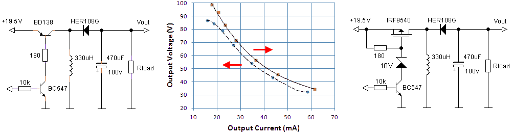
Figure 9.1 Testing of a bipolar and MOS version of the negative power supply.
Figure 9.1 shows the two converter circuits tested. The timing signal driving the BC547 transistor was generated by my pulse generator set at a pulse width of 20 us at a repetition rate of 10 kHz and an amplitude of 0 – 5 V. These conditions are identical to the output pulses of the micro-controller when it is driving the converter for maximum output voltage. The circuit with the bipolar transistor is identical to the circuit used in the V2 uTracer. The version with the pMOS transistor is almost identical with the exception that a zener diode was added to limit the maximum gate-source voltage to 10 V. The circuits were tested by applying different load resistors and recording the corresponding output voltage and current.
As expected the circuit with the pMOS transistor performed slightly better than the circuit with the BD138 (Fig. 9.1 center). Especially at lower currents (higher output voltage) the MOSFET version was significantly better. However, for an output voltage of –40 V the difference was so small that I will just stick with the bipolar version, especially since efficiency is not an issue here. Note that I replaced the 1N4148 diode from the original uTracer circuit with a fast switching HER108G diode. It didn’t give any improvement, but I think the HER108G is a bit more robust in this circuit, while it is still one of the cheapest diodes of its kind available.
Monitoring the grid bias
Apart from the fact that skipping a whole boost converter saves a lot of “real estate” on the PCB, it also releases one of the analog AD-converter inputs from the microcontroller so that it can now be put to better use! One of the options is to really monitor the grid bias during the measurement pulse. You will recall that in the present design the grid bias is set by programming one of the PWM generators on board of the controller. We then have to rely on a proper functioning of the electronics to make sure that the correct grid bias is really set. It would be nice to have a way to check the proper functioning of this circuit.
The AD converter input covers a voltage range of 0 to 5 V. If we take the ground of the microcontroller as a reference, then the grid bias ranges from 19.5 V to -40 V. The reason for this is of course that the cathode of the tube is referenced to the power supply voltage. So we need a circuit than can map an input voltage of -40 V to 20 V to 0–5 V. It appears that three resistors can do the job.
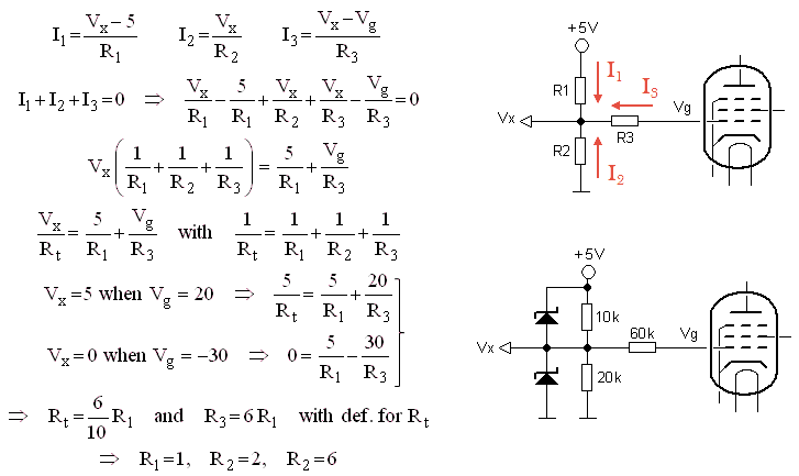
Figure 9.2 Design of a three branch voltage divider circuit to monitor the grid bias
The top circuit in Fig. 9.2 shows a three branch voltage divider circuit. One branch is connected to +5V, one branch to Gnd and the third branch is connected to the grid. Note that the circuit which takes care of actually generating the grid bias is not shown in this figure. The central node denoted here by Vx is connected to the AD input of the micro controller. Without R3, R1 and R2 will set Vx so some value between Gnd and 5 V. The question now is how to pick values for R1, R2 and R3 in such a way that when Vg is 20 V, Vx will be pulled up to 5 V, while when Vg is -40 V, Vx will be pulled down to Gnd. First the currents I1, I2 and I2 flowing through the resistors are calculated for a certain Vg and Vx. According to Kirchhoff’s Law the sum of all the currents flowing to a certain node has to be zero. From this we can derive an equation which gives Vx as a function of Vg in which R1, R2 and R3 are “unknowns”. We know two Vg and Vx pairs which have to satisfy the equation: (Vg,Vx)=(20,5) and (Vg,Vx)=(-40,0). Substituting these datapoints into the equation we find two relations which give R2 and R3 when R1 is known. We can now simply pick a value for R1 that will set the current levels in the voltage to an acceptable level e.g. R1 = 10k, we then find R2 = 20k and R3 = 60k. Finally two Schottky diodes are added to protect the micro-controller input from any over or under voltage conditions which might arise from improper functioning of other parts of the circuit. At this moment I am not sure if I am going to implement the grid bias monitor, perhaps I want to use the analog input for something else. Nevertheless I added the calculation here for my personal documentation.
| to top of page | back to homepage | to part I |
One of the most important tube parameters is the transconductance. The transconductance tells you something of the intrinsic capability of the tube to amplify signals. The transconductance is defined as the ration of the variation in anode current as a result of a small variation in grid voltage at a certain bias point. The unit in which the transconductance is expressed should be A/V or S (from Siemens). Typical transconductance values range from 0.001 to 0.015 A/V. I have noticed that in Europe the transconductance is usually specified in mA/V, so that typical values range from 1 to 15 mA/V. In the US it is more common to express the transconductance in “mho”, which is “ohm” written backwards. So 1 A/V = 1 S = 1 mho. Rather than expressing the transconductance in millimho’s is has become custom to express it in micromho (1000000 micromho = 1 mho) so that the typically transconductance range becomes 1000 – 15000 micromho.
There are basically two ways to measure the transconductance. In the first method the anode current as a function of the control grid bias is measured and plotted. To find the transconductance at a certain bias point, the tangent line to the curve is constructed at that bias spoint.
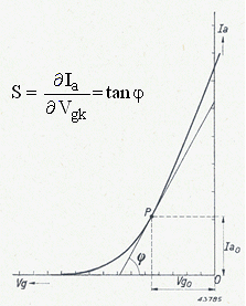 The transconductance is the slope of the tangent line. It is actually this method that I had planned to use for the uTracer V3. The Idea I had was to measure the Ia(Vgk) curve, interactively fit a best polynomial through the measured data, and then analytically determine the slope of the curve in every point. In this way any measurement noise is suppressed and a nice smooth transconductance curve is obtained.
In the second method the transconductance is obtained under real AC conditions. A small AC signal is added to the grid bias and the corresponding AC anode current is measured. The transconductance is found by dividing the amplitude of the anode current by the amplitude of the AC grid voltage. An example of a transconductance tester which works this way is the RAT tube tester designed by Steve Bench. Now, certainly for frequencies which are so low that inter-electrode capacitances, and the time it takes for the electrons to travel through the vacuum of the tube can be neglected, both methods should yield exactly the same result. However, in the world of electron tubes exact science very often has to compete with emotions and feelings. So it is therefore not surprising that there is a large school of people who definitely swear to especially the AC method. Although I am myself convinced that indeed both methods should yield exactly the same result, I nevertheless spend the past weeks thinking if and how an AC transconductance test could be included in the uTracer V3 as an option. I summarize the main ideas here in this section for my documentation. The circuits presented in this section were not tested, they are at this moment just “paper ideas.”
Before drawing schematics, let’s look at some figures. As mentioned the transconductance of most tubes varies between 1 mA/V and 15 mA/V. On the lower side we find e.g. some of the battery tubes: DL91 1.57 mA/V @ 8 mA, or the DL96 with 1.4 mA/V @ 5 mA. On the higher side we find many of the popular audio amplifier tubes: EL84 11.3 mA/V @ 48 mA, EL34 11 mA/V @ 100 mA and the EL38 with 14.3 mA/V @ 100 mA. But these are transconductances at the optimal bias point. To measure a full transconductance curve the tester should be able to measure also transconductances which are considerable smaller, say at least a factor of 10, so down to 100 uA/V, preferably smaller. On the high side we will assume a maximum transconductance of 30 mA/V. The amplitude of the AC voltage that is applied to the control grid has to be sufficiently small to assume small signal operation. A common value that is used is 100 mV(pp) (top-top). This means that the amplitude of the anode current will range from 10 uA(pp) to 3 mA(pp).
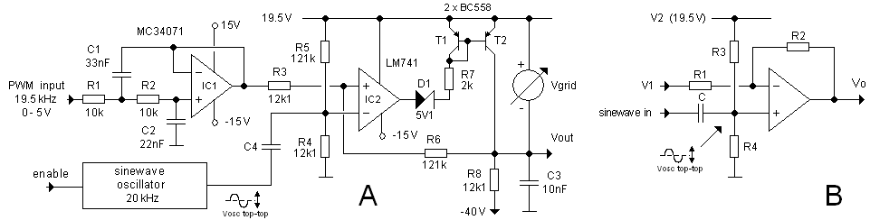
Figure 10.1 Injection of the AC signal into the grid bias circuit.
Before we look at the problem of how to measure the AC component in the anode current, we first have a look at how the AC voltage can be added to the control grid. The first question that needs to be answered is what frequency to use for this AC signal. Most commonly a 1 kHz signal is used. However, in the utracer the length of the measurement pulse is 1 ms which would amount to one period of the AC signal. The frequency of the AC signal should be as high as possible, but still in the audio range. I thought 20 kHz would be still an acceptable value. At that frequency exactly 20 periods of the AC signal fit into the length of a single measurement pulse. My first idea was to let the microcontroller generate a 20 kHz square-wave signal and then use an active 20 kHz bandpass filter to turn it into a sinusoidal signal. A much simpler solution is to use a simple fixed frequency single transistor phase-shift oscillator that can be turned on and off by the microcontroller.
Figure 10.1A depicts how the sinusoidal signal is injected into the control grid bias circuit. The advantage of injecting the signal at the negative input of the OpAmp is that at this point we have a constant and well defined impedance of 12.1k//121k = 11k so that the amplitude of the AC signal is independent of the control grid bias. To calculate the amplitude of the signal we have to inject to obtain an amplitude of 100 mV on the control grid, the equivalent circuit of Fig. 10.1B is used. Here the high voltage driver stage consisting of T1/T2 are assumed to be part of the OpAmp. Since this stage the inverting and non-inverting inputs of the OpAmp in Fig. 10.1B are exchanged compared to Fig. 10.1A. We find the relation between the output voltage and the input voltages by firsts finding the relations for the voltages at the inverting and the non-inverting inputs of the OpAmp and then equating these relations:
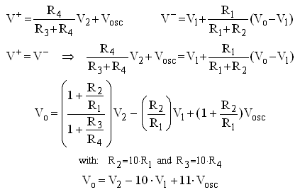
Observe that the amplitude of the AC component in the grid voltage equals 11*Vosc. So for 100 mV amplitude grid bias a signal with an amplitude of 100 mV / 11 = 9 mV has to be injected.
Measuring the AC component of the anode current during the measurement pulse is less trivial. Figure 10.2A depicts the most straightforward approach. As recalled, the DC anode current is measured across a small resistor between ground and the high voltage buffer capacitor. Naturally also the AC component of the anode current will appear across this resistor. The AC component may be obtained by simply decoupling it from the DC component with a suitable capacitor. Some rudimentary showed that this option will work, however the magnitude of the AC signal is very small. The reason is that the value of Rs is fixed by the DC measurement requirements. Assuming a maximum current of ca. 150 mA, the value of Rs will be ca. 30 ohm to obtain a full scale input for the AD converter. With an AC anode current as small as 10 uA(pp), this will give an AC voltage as small as 300 uV(pp). Measuring a signal with such a small amplitude in a 1 ms time frame is possibly not un-do-able, but it is far trivial.
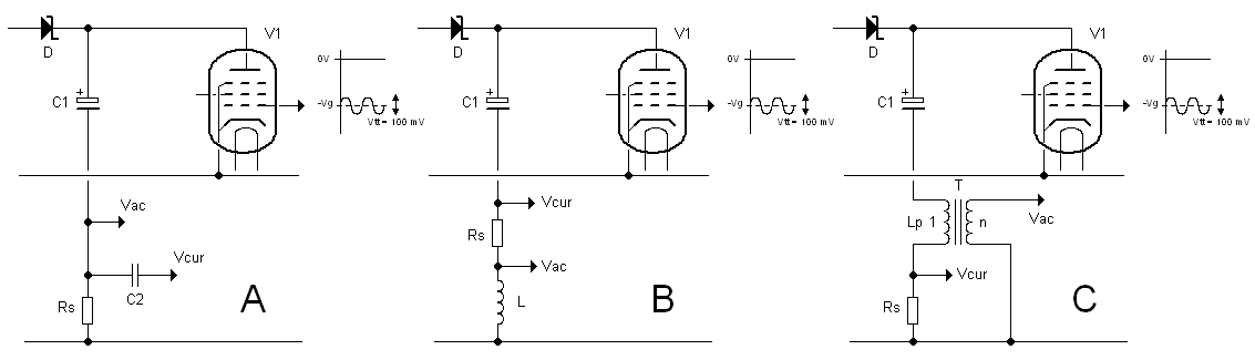
Figure 10.2 Three ways to retrieve the DC and AC components from the anode current.
It would be great if there was a way to obtain a larger AC signal. The simplest way to do that is to measure the AC component across an inductor (Fig. 10.2B). The impedance of 1 mH inductor at 20 kHz for instance is already 2*pi*f*L = 125 ohm. This is already a factor 5 improvement. However, there are (at least) two arguments against pursuing this route. In the first place one has to realize that the inductor also has to “digest” the transient from the measurement pulse itself. The larger the inductance value, the more time it will take for transient voltages to settle. The other argument is more serious: using a setup as shown in Fig. 10.2B the measured AC signal will be the sum of the DC and the AC signal. Although it may be possible to disentangle them again, it is messy and reminds me of all the offset and drift problems I had with the V2 uTracer.
By far the best solution is to replace the inductor by a transformer (Fig. 10.2C). This has two huge advantages: by connecting one side of the secondary turn to ground, both the (pulsed) DC as well as the AC components of the current can be decently measured with respect to ground. Secondly by using a turns ratio >1 an offset free “amplification” of the AC voltage is obtained! I know that transformers are extremely un-popular among amateur (and I guess also many professional) electronics enthusiasts. However things are not as bad as they seem. The German company Wuerth Elektronik produces a large range of flyback transformers among them some very suitable types. An example is the LT3748 (Wuerth manufacturing code 750311486), which can be ordered from Farnell (Farnell product number 1895729). This tiny transformer has a primary winding of 100 uH which saturates at 2 A. It has secondary windings which each have a turns ratio of 10 with respect to the primary winding. So by placing the secondary windings in series a 1:20 turns ratio can be obtained. The impedance of the 100 uH primary turn at 20 kHz is 2*pi*f*L = 12.5 ohm, the transformer will “up-transform” the voltage drop over the primary inductance by a factor of 20. A 10 uA(pp) anode current will now appear as a 2.5 mV(pp) signal which starts to appear do-able. Before looking more into detail in the working of the transformer, let’s first have a look at how the rest of the measurement circuit could look like.
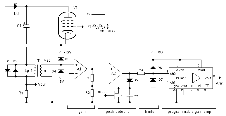
Figure 10.3 Detection of the AC anode current.
One of the simplest ways to measure the amplitude of the AC signals is probably to use a simple peak detector. Figure 10.3 represents the basic layout of such a circuit. First the still rather small signal from the transformer is amplified by the high input impedance amplifier circuit around A1. The circuit around A2 is basically a combination of a peak detector and a sample and hold. When T1 is open, OpAmp A2 continuously compares the voltage on the capacitor with the input voltage. When the input voltage is higher than the voltage on the capacitor the capacitor is charged via D5 until both voltages are equal again. When the inout voltage is lower than the voltage on the capacitor, the output of the OpAmp becomes negative. Diode D5 is now blocking so that the voltage on the capacitor will remain constant. By switching on T1 the capacitor can be discharged. The idea is to leave T1 switched on well into the measurement pulse until we are sure that all the transients as a result of the measurement pulse have died out and then to open it so that the peak values of the signal can be obtained. Since the measurement frequency is 20 kHz, we know for sure that after 50 us the peak value is stored. AD conversion should take place within the measurement pulse to skip the transients at the end of the measurement pulse. The peak value
Obtained this way is further amplified with the same Programmable Gain Amplifier that was used to measure the DC current, but this time using the second input channel. Assuming that the maximum transconductance to be measured is 20 mA/V, and using a 100 mV(pp) AC grid signal, an AC anode signal of 2 mA(pp) is obtained. Using the 100 uH 1:20 transformer this will result in a voltage at the input of A1 of 500 mV(pp). With a gain of about 10x this would just result in a full scale readout of the AD converter. Assuming an input offset voltage of 15 uV for OpAmp A1 this will result at an output offset voltage of 150 uV, which is a factor 10 lower than the minimum expected input signal, in other words not too serious. A transformer with a somewhat higher primary inductance and higher turns ratio would have helped enormously to further reduce the offset in the lowest measurement range. Unfortunately I could not find such a transformer as an of-the-shelf component, but perhaps when all this works so far, I will make one myself.
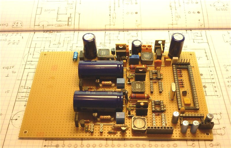
Figure 10.4 Christmas 2011! This project is now underway for exactly a year. The project is actually one of the most interesting projects I have ever undertaken. It combines everything: analog / digital electronics, assembler and high-level programming, and above all vintage radio-tube technology. For me personally it has been a turbulent year, but this project has brought some sense in my life and kept me going. The past weeks have been spent cleaning up my “laboratorium” as I always call my hobby room at home, and I am now spending a very quiet en peaceful X-mass holiday assembling the version 3 uTracer, which is making excellent progress!
| to top of page | back to homepage | to part I |
In section Fully interrupt based boost converter control
(Part I) it was explained how the boost converters can be controlled by an interrupt routine which runs completely in the background. In this way we don’t have to concern ourselves with the control of the boost converters in the main program, and they can remain “on-line” all the time thereby eliminating some of the problems encountered in the version 2 of the uTracer. In the mean time the routine has been written and is functioning satisfactory. It has become however a rather complicated piece of programming and I know that if I don’t document it now immediately, I will have the greatest difficulty “re-inventing” it later on. So therefore, mostly for my own documentation, a description of the working of the routine and the variables that interface with it.
Figure 11.1 Mapping of the boost converters on the I/Os of the micro-controller.
Since the writing of “Part I” things have changed in the sense that we have one negative power supply less to deal with, although that not really makes a difference since the “boost converter interrupt routine” can deal with up to eight converters simultaneously. From the point of view of the software, a boost converter is nothing more than a black-box
with a digital pulse input and an analog output voltage. When the analog output voltage is below a certain set-point, the pulse input needs to pulsed until the output voltage is above the set point. The pulse width I use here is 20 us (although I might change it to 30 us in a later stage) and the repetition frequency of the pulses is 10 kHz. The analog voltages are measured by the AD converter on the microcontroller. Each boost converter thus requires a separate analog input. The output pulses are
 available on one of the I/O ports of the PIC controller. As a result of how the software is organized these pulse outputs have to be located on the same output port. For the uTracer 3 I have chosen to use the lowest 3 bits of PORTB, since most of the higher bits of this port are already in use for the in-circuit programming interface. Fig. 11.1 summarizes the connections to the PIC for the three boost converters.
As mentioned before control of the boost converter is performed by an interrupt service routine which is called on a timer 0 overflow every 100 us (the 10 kHz repetition rate). It will be recalled that also in the version 2 uTracer the boost converters were controlled by an interrupt routine, however, in that case the interrupt routine only generated the pulses; the decision whether or not pulses need to be generated (so the AD conversions and the comparison of the AD results with the set-points) was done by the main program since at that time I thought it would be impossible to also do that in the interrupt routine. This caused a lot of problems. In the “Part I” section on this topic, I explained how the AD acquisition can be inter-weaved with the pulse generation. What it boils down to is that the pulse time (20 us), which is time actually consumed by the interrupt service routine and which in the version 2 software was “burnt” in a delay loop, is now used to let the AD converter settle to a new input selection and to do the comparison of a previous AD conversion to the set-point value. Next to this the time in between the pulses, which is time used by the main program, is used to do the AD conversion for the next boost converter. The interweaving of the pulse generation and the processing of the AD results requires that the routine is optimized for speed. This means that several tricks have been used e.g. to eliminate unnecessary branching. Another difference with the version 2 software is that the routine which discharges the boost converter capacitors has been disentangled from the boost converter routine. In the end that made more sense, is more transparent and requires less overhead.
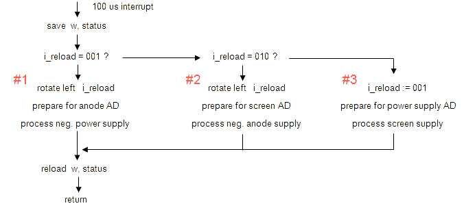
Figure 11.2 High level overview of the interrupt based boost converter service routine.
Figure 11.2 gives a high level overview of the boost converter interrupt routine. As mentioned it is called very 100 us. The first thing which is done is that the W and STATUS registers are saved. Next one of three pieces of code (a cycle) is executed. In this case there are three cycles since there are three boost converters to service. A counter ensures that upon every call to the interrupt routine a new cycle is executed. For this counter I used a rather out-of-the-way construction. Instead of incrementing an integer and performing a comparison of two numbers at the beginning of every cycle I used a shift register construction. The shift register I_ROTATE is loaded with 00000001 at initialization and the 1 is shifted one position to the left after every cycle. In this way only a simple “btfss” instruction is required to check if a cycle has to be executed or not. In the end it turned out to be a bit more complicated since we have to make sure that the carry bit is cleared before every shift operation. Perhaps if I had to rewrite the routine I would use a normal counter, but anyway it is functioning very satisfactory this way.
The different cycles resemble each other in the sense that in each cycle the outputs are pulsed if needed. However, in every cycle a different AD conversion is started while also in each cycle the data for a different boost converter is processed. At the start of cycle 1 e.g. the AD conversion result for the negative power supply is available (the AD conversion was started the previous cycle) so that the result can be compared to the set-point. In parallel to this the AD converter is already prepared to sample the anode supply.
The boost converter interrupt routine communicates with the main program via a number of variables. In the first place the main program has to store the 10-bit set points for the negative power supply, the anode supply and the screen supply in variables (NP_SET_H:NP_SET_L), (A_SET_H:A_SET_L), and (S_SET_H:S_SET_L) respectively. Next the boost converter is controlled via four control bytes:
The correct procedure for setting the anode- or screen boost converters to a new set-point should comprise the following steps: first make sure the boost converter is disabled by resetting the corresponding bit in BST_ENBL. Next modify the set-point value. Since the buffer capacitor can have been charged to a value higher than the set-point during a previous measurement, we now first have to discharge it until we are sure the buffer capacitor voltage is lower than the set point (click for more info). This has to be done by the main program, but it can use the information in BST_MSK to see if the voltage is higher of lower than the set-point. There is a snag here: as mentioned it takes at least three cycles to make sure BST_MSK is properly updated. The optimal procedure is that the main program issues a 1 ms discharge pulse regardless of the status of BST_MSK. The discharge pulse is used to charge the pulse capacitor but also serves as the delay to ensure BST_MSK is updated. After the 1 ms discharge pulse, the main program should continue discharging the buffer capacitor until the proper bit in BST_MSK becomes reset. Next the BST_OK bit is cleared and the converter is enabled by setting the bit in BST_ENBL. When all BST_OK bits become set again, all boost converters have reached their set-point and a measurement pulse can be issued.
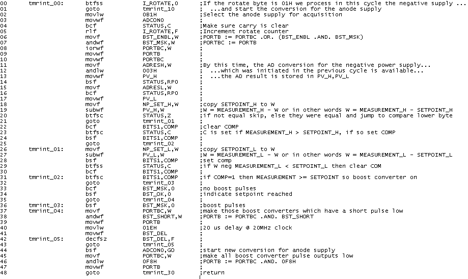
Figure 11.3 Cycle 1 code example.
Finally, for the purpose of documentation let’s analyze the code of one of the “cycles.” Figure 11.3 gives the assembler code for the #1 cycle which controls the negative power supply.
| to top of page | back to homepage | to part I |
Finally I have arrived at the stage where the whole thing can be assembled and tested. It has been a busy year, and the Christmas holiday (2011) was the perfect moment to unwind myself a bit by filling a perfboard with good-old through-the-board components. Personally I think that SMD components are just horrible. They make experimenting extremely
 difficult and take all the fun out of the hobby. Fortunately I have spent the last 20 years building up a stock of “normal” components that will hopefully last until my hands will shake so much that only thing left will be reading these pages. I have already argued that with a rather big project like this, it is better to build and test the circuit in parts. Especially the interplay between hardware, firmware and user interface makes the chances for a huge disappointment when the whole project is tested at once almost 100%. The first parts that were built were the processor with ICP and RS232 interfaces and the filament driver. The filament driver was tested using a separate pulse generator as input. It functioned perfectly as before, and had no problem at all in regulating a 6.3 V, 1.5 A filament, corresponding to an EL34. Also the negative power supply was tested using an external pulse generator. As expected it presented no problems.
The next circuits to be assembled were the high voltage boost converters and the high voltage switches. Before they were tested, first the new interrupt service routine which controls the boost converters was written (see previous section). This was a tricky bit of programming and took a few days, but without too much problems worked very satisfactory.
The discharge circuit
The next part to be tested was the discharge circuit. It will be recalled that whith respect to the V2 uTracer, the firmware which controls the discharging of the buffer capacitors was removed from the interrupt routine and included in the main program. A charge cycle now contains the following steps:
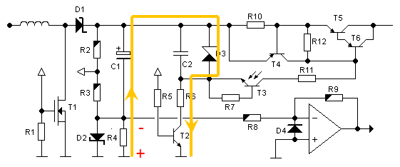
Figure 12.1 Voltage drop over the current sense resistor as a result of the discharging of the buffer capacitor.
During the testing of this sequence a rather curious problem was encountered. When a sequence of voltages was programmed e.g: 50, 100, 150, 50, 100, 150, it appeared from the values returned by the uTracer that during the second series the first voltage was a bit higher than the set-point, e.g.: 58 V instead of 50 V. It was always the second and subsequent series which returned a too high value. A few hours were spend searching for the cause of this strange problem. Obviously at first the software was suspected. Checking the firmware line-by-line and adding numerous breakpoints eventually revealed that when the buffer capacitor voltage was measured during discharging, the discharging was stopped at a too high voltage. I was so convinced that this was a software problem that I didn’t even consider the possibility that the cause could also have been located in the hardware. And that in the end turned out to be the case! When the discharge transistor T2 (Fig. 12.1) is switched on, the discharge current will obviously flow through the current sense resistor R4. This will cause a voltage drop over R4 with a polarity as indicated. The voltage drop will lower the voltage measured by the high voltage divider circuit (R2 and R3). The buffer capacitor voltage will therefore appear to be lower than it really is.
This was something I had absolutely overseen. Fortunately the problem could be solved completely in software. The solution is simple: switch off the discharging on the exact moment the voltage is measured. It was simply implemented by inserting an instruction in between lines 01 and 02 in the code listed in Fig. 11.3 which switches of the discharging. To continue the discharging after execution of the interrupt routine, the discharging is continuously restarted in the loop in the main program which coordinates the discharging process.
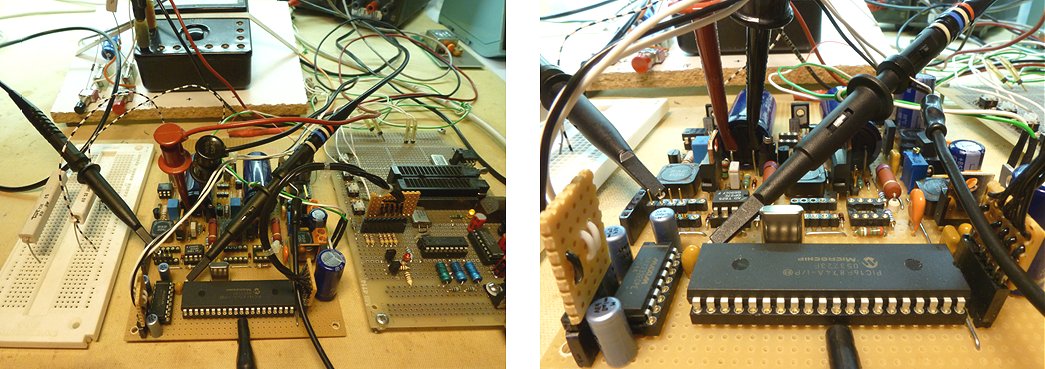
Figure 12.2 Boost converters “under-test.”
Testing the over-current switch-off circuit.
In sections 5 and 6 it was explained that “the short circuit protection,” or more in general “the over-current protection,” consists of two components. In the first place a simple hardware circuit which limits the current to approximately 250 mA. But even when the current is limited and the measurement pulse is only 1 ms, this still results in a destructive dissipation in the high voltage transistor. A second protection mechanism therefore switches off the high voltage the moment an over-current condition is sensed. The mechanism consists of a comparator on board of the micro-controller which compares the voltage drop over the current sense resistor with a programmable voltage reference which is generated on-chip (Fig. 5.3).
Figure 12.3 Manipulation of interrupts around the measurement pulse generation part.
As soon as the comparator detects an over-current condition, an interrupt is generated which switches off the high-voltage. Normally timer0 generates an interrupt every 100 us so that boost converters can be serviced. As it happens, the boost converters are shut-down during the actual measurement pulse to minimize the noise in the system. During the time the boost converters are off, the interrupt is redirected so that the high voltage switches are switched off. This requires some fiddling with interrupts which is illustrated by the code example in Fig. 12.3. The code is pretty straightforward. A change of the output of one of the comparators causes an interrupt. To reset the interrupt generating condition a dummy read to CMCON is needed. Flag INTSEL is set to communicate to the interrupt service routine that the interrupt was caused by a change of output of one of the comparators.
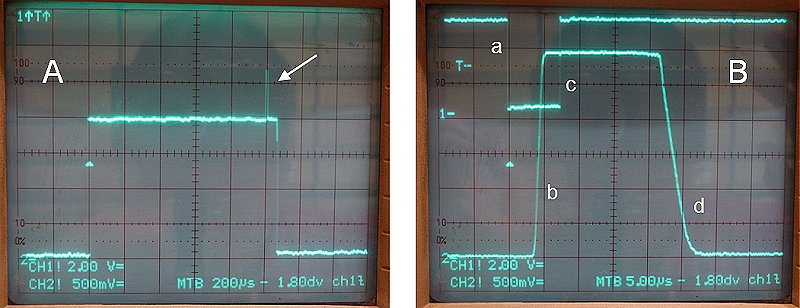
Figure 12.4 Spikes on the measurement signal as a result on ADC MUX switching (left), current protection circuit in action (right). See also text below.
During testing of the circuit a rather unexpected phenomenon was encountered. During the first test the anode current was measured halfway during the 1 ms measurement pulse. Referring to the code example of Fig. 12.3, the difference was that the call to AD_AC, which samples the anode current, was performed in between two 0.5 ms delay loops. For currents well below the set compliance current everything worked as expected. However, as the measured current approached the current limit, the measurement pulse was sometimes halved! This obviously had something to do with the analog sampling of the anode current. What happened was when the analog input MUX was directed to the anode current input, this induced a spike on the input voltage, due to the charging of the sample-and-hold capacitor. The effect was rather pronounced as a result of the relative high impedance of the external circuit due to R4 (Fig. 5.3). Figure 12.4 (left) shows how the spike was captured on the memory-scope. It also appears in the movie below at 3’4”. To solve the problem the current measurement was moved to the end of the pulse which was reduced in length to 0.5 ms (Fig. 12.3). This also reduced the discharging of the buffer capacitor for high currents. Additionally the current protection was switched off during the actual current measurement by disabling interrupts (line 16). So during the last 20 us of the total measurement pulse, the over current protection is off; since this is very short it should not pose a problem.
Figure 12.4 (right) shows the current protection circuit in action. The upper trace shows the signal used to drive the LED in the opto-coupler of the high-voltage switch, while the bottom trace is the input voltage to the current protection OpAmp on-board of the micro-controller. At point (a)the microcontroller switches on the high-voltage switch on. About 4 us later the high voltage switch responds, and a current starts to flow (b). Immediately an over-current condiction is detected and within 2 us the controller switches of the high voltage switch (c). It then takes ca. 15 us for the high voltage switch to respond and the current is interrupted (d). These results are in perfect agreement with the results obtained with the breadboard circuit.
The circuit so far worked so beautiful that I could not resist posting a short movie showing the testing of the over current protection.
Testing the Programmable Gain Amplifier.
Working with the version 2 uTracer, I quickly experienced that one of its most irritating limitations was the lack of a comfortable measurement range selection. We are all spoiled by working with oscilloscopes where our wise forefathers have found it convenient to scale measurement ranges as: 1-2-5-10–20–50–100-… In section 5 the PGA113 “programmable amplifier” from TI was introduced. Normally I prefer to design my circuits using “easy” components which I can just pull from my rather extensive stock of components. However, in this case it would have been foolish not to make an exception. The PGA113 is exactly the perfect component to realize “oscilloscope type” ranging for the uTracer, and on top of that it only costs a few euro. Its only drawback is that it only comes in an impossible small package!
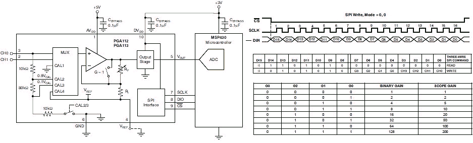
Figure 12.5 Functional diagram of the PGA113 and SPI protocol.
Figure 12.5 shows the block diagram of the PGA113. The circuit has rail-to-rail inputs and outputs (well almost). When Vref is tied to ground, the circuit basically behaves as a non-inverting amplifier with a transfer function given by Vout = G*Vin, with Vout and Vin measured with respect to ground. The gain can be set to 1,2,5,10,20,50,100 and 200. Programming of the gain is done with a SPI (Serial Peripheral Interface). The protocol is very simple, first the chip select (CS) line is made low to select the PGA113. Next 16 bits are clocked into the PGA113 on every rising edge of the clock input, the most significant bit first (Fig. 12.5). When the first byte is 2A Hex, this signals the PGA113 that the next byte will set the gain and the selected input channel. Figure 12.5 summarizes how a gain can be selected. The PGA113 has two input channels. Normally channel 1 is used. Channel 0 can be used as an additional input channel, or is can be used in an on-chip offset calibration procedure. I do not use the offset procedure, but have reserved input channel 0 for the dynamic transconductance measurement option. The microcontroller has an on-board SPI interface, but I preferred to write a small routine which “bit-bangs” the SPI bits to an output. Routine “spi_anode” writes “2A + SPI_ANODE” to the anode PGA113, while “spi_screen” writes “2A + SPI_SCREEN” to the screen PGA113.
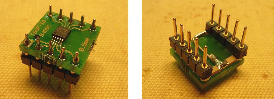
Figure 12.6 An adaptor PCB connects the SMD world to the more standard “DIL dimension” world. Two 100 nF SMD capacitors are used to decouple the both the analog and the digital supplies of the PGA113 as close as possible to the actual device.
Fortunately there are adaptor PCBs so that it is still possible to use these tiny components on a normal perfboard. I have worked with SMDs before, but this was really the first time that I had to use a microscope! Nevertheless, the whole circuit worked like a dream. In the initial tests, a 27 ohm current sense resistor was used. This implies that at a gain of 200, 5 V full scale input to the AD converter corresponds to 5 / 200 = 25 mV voltage drop over the current sense resistor corresponding to 0.025 / 27 = 926 uA! For this range the signal appeared to be a bit noisy (Fig. 12.7 left). In retrospect this is not surprising. Even my very nice PM2534 Fluke multi-meter is “noisy” in this measurement range when no averaging is used.
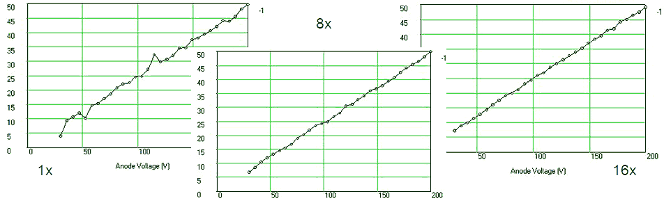
Figure 12.7 First measurements using the PGA113 set to a gain of 200X. The load was a 800k resistor to that the current at 200 V amounted to 250 uA (values on the y-axis have no meaning). I the left figure no averaging was used, in the center figure the measurement was averaged 8X in the right figure 16X.
Basically there are (at least) two ways to tackle the noise problem: averaging and bandwidth reduction. The simplest method is averaging which can be completely implemented in software. As it turned out it was even very simple to implement it. The measurement routine which normally writes the (10 bit) current measurement to two (high/low) output bytes was modified so that it added the measurement to the output bytes rather than just copying it to it. So by calling the measurement routine e.g. 8 times, the output bytes contain the sum of the eight measurements. Figure 12.7 shows three exactly the same measurements in which: no averaging was used (left), or the measurement was averaged 8x (middle) or 16x (right). The current values along the y-axis are arbitrary because the GUI was not modified yet for the new hard- and firmware. However, since a 800k resistor was measured, full scale corresponds to 200 / 800.000 = 250 uA.
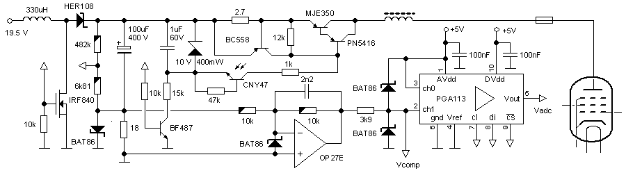
Figure 12.8 The addition of a small 2n2 capacitor across the feedback resistor over the OpAmp greatly reduces the measurement noise.
The other method to reduce noise is to limit the bandwidth of the measurement system. In first instance no bandwidth limiting measures were taken so that the overall bandwidth must have been quite large (I don’t know exactly how large). All the noise over this band contributed to the observed the current fluctuations which were observed. However, there is no need at all for such a large bandwidth. The only requirement is that the current reaches its steady state value well within a millisecond. The simplest way to reduce the bandwidth is to shunt the resistor in the return path of the inverting OpAmp with a capacitor to give it a low pass characteristic. With my simple MicroCap circuit simulator I verified that with 2.2 nF the rise time of the current is such that it settles within 0.3 ms.
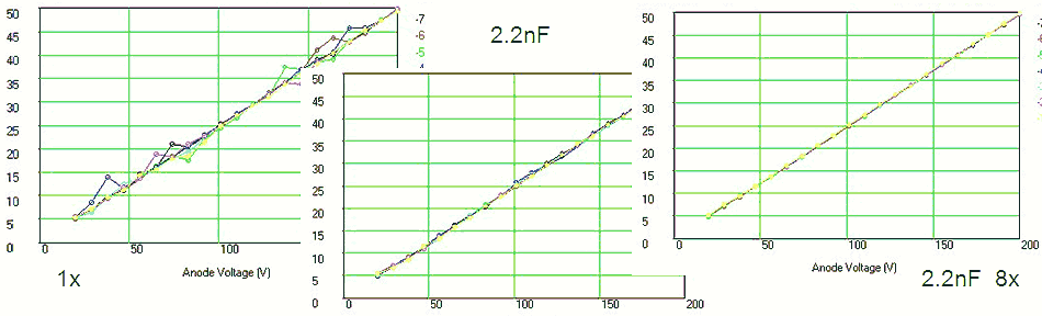
Figure 12.9 Measurements using the PGA113 set to a gain of 200X. The load was a 800k resistor to that the current at 200 V amounted to 250 uA (values on the y-axis have no meaning). I the left figure no averaging or bandwidth reduction was used, in the center figure the bandwidth was reduced by adding a 2n2 capacitor over the feedback resistor of the OpAmp, in the right figure next to the bandwidth reduction also the measurement was averaged 8 X.
The addition of the small capacitor resulted in a very significant improvement of the noise behavior of the circuit. The left graph in Fig. 12.9 shows 7 consecutive I-V measurements of a 800k resistor without the 2.2 nF capacitor. In the center graph of Fig. 12.9 the capacitor was added. Finally, in the right graph of Fig. 12.9 the same measurement was repeated but now the measurement was 8 times averaged. The curves are so identical that the light color of the last one nearly obscures the first 6 measurements. All in all not a bad performance for such a simple circuit!
Bits and Pieces
The last parts to be tested were the filament supply, the grid bias circuit and the “cathode” circuit. The cathode circuit is the new construction which allows measurements down to zero volt anode and screen bias. Several safety features were included into the circuit to protect the uTracer against short-circuits and flash-overs.
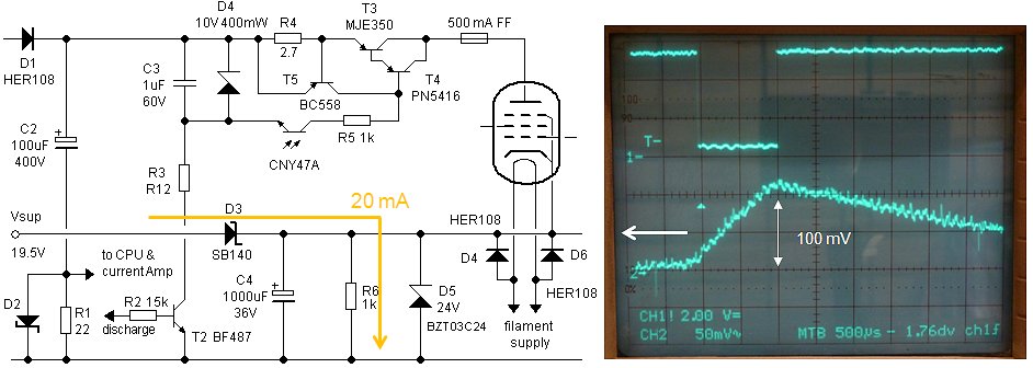
Figure 12.9 The modified cathode circuit and a measurement of the cathode potential rise as a result of a 100 mA current measurement.
In the original circuit depicted in Fig. 8.1 transistor T6 was used to discharge buffer capacitor C4 which stores the charge released during a measurement pulse or a flash-over. In the final circuit shown in Fig. 12.9 (left) the transistor was replaced by a fixed 1 k resistor (R6, Fig. 12.9). The resistor draws a constant current of at least 20 mA. This current discharges C4 at a rate of 20 V/s (20 mV/ms). Additionally, the constant current ensures a minimal voltage drop over isolation diode D3 for low cathode currents. The upper trace in the oscilloscope image depicted in Fig. 12.9 shows the measurement pulse signal generated by the micro-controller. The falling edge of this pulse was used to trigger the memory-scope. The lower trace shows the cathode potential with repect to ground. In this measurement the anode current was 100 mA. The expected voltage increase is: V = (I*t)/C = (0.1*0.001)/0.0001=0.1 V, exactly what is measured. Observe that also the discharging of C4 very nicely corresponds with what we expect (20 mV/ms).
Figure 12.10 (left) shows a voltage-current measurement using a 2k resistor as load. The voltage was swept in this case between 2 and 200 V. There is a very practical reason that the lower limit for the anode voltage was set to 2 V instead of 0 V: when for a new voltage sweep the buffer capacitor is discharged, the voltage measured by the controller is subjected to an inaccuracy caused by tolerances in the resistive voltage divider and the 5 V power supply which is the reference for the AD converter. It is therefore not unthinkable that the controller measures a voltage which a fraction too high. For voltages well above the power supply this is not a problem, it just causes a small offset. However, for voltages very close to the power supply it can happen that the controller wants to continue to discharge the capacitor (because it measures a slightly too high voltage) while this is not possible because the buffer capacitor voltage cannot decrease to a value below the supply voltage. It appears that a margin of 2 V is enough to solve the problem. Despite the fact that there is a small problem for voltages lower than 2 V, it is quite straightforward to discharge the capacitor to the point that it is clamped to the supply voltage. This can be done by simple adding a second or so to the discharge cycle. What I think I will do in software is simply map all voltages between 1 and 2 V to 2 V, and all voltages between 0 and 1 V to 0 V.
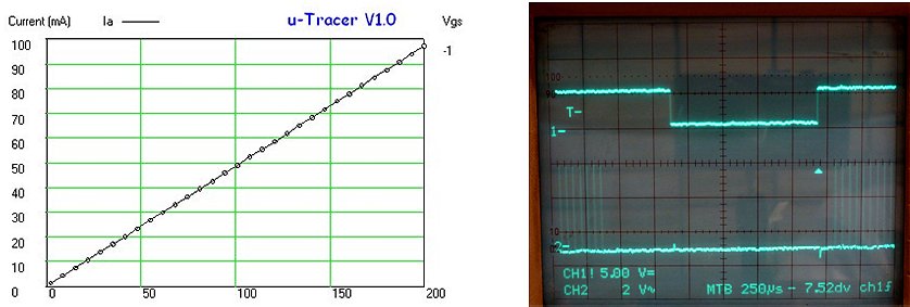
Figure 12.10 (left) I-V curve 2 – 200 V of a 2k resistor, (right) the PWM signal which drives the filament circuit is disabled during the measurement pulse.
There is little to say about the grid-bias and filament driver circuits except that they functioned as expected. Figure 12.10 (right) shows on the upper trace the measurement pulse and on the lower trace the PWM signal which drives the filament supply. The PWM pulses are quite small (11%) since in this case the filament voltage was 6.3 V. To minimize the noise during the measurement pulse, the filament driver is shut down for the duration of the measurement pulse. This is simply done by making the PWM output temporarily an input.
| to top of page | back to homepage | to part I |
After all this planning and testing the final circuit diagram is slowly getting its final shape. Figure 13.1 shows the most recent version, and even in this version some things, such as the connections of the various parts to the IO ports of the micro-controller have not fully crystallized yet. When there is a new version of the circuit diagram I will update the circuit diagram with the date on the circuit diagram serving as a version number.
Figure 13.1 Most current version of the circuit diagram of the analog part of the uTracer version 3.
At first sight the complete circuit might look a bit intimidating. However, in reality it is not more than a hand full of discrete components and a few ICs. Most components have been selected for low-cost and availability (from Farnell). Despite the fact that the circuit occupies significantly less (perf-board) real estate compared to the version 2 uTracer, it offers a significantly better performance and has many added features, such as programmable sensitivity and programmable over current protection.
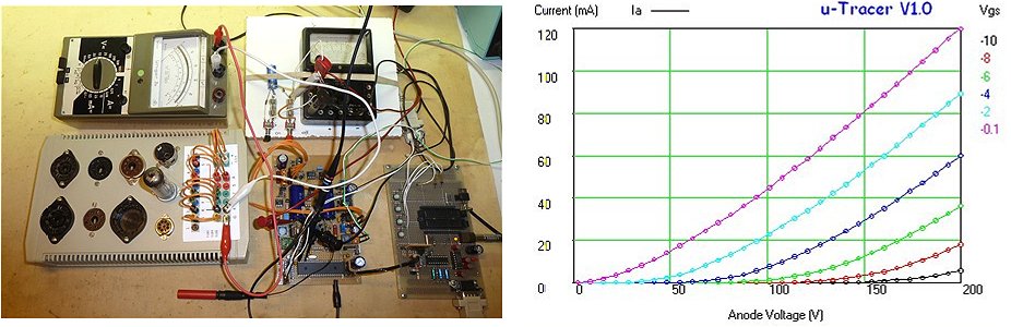
Figure 13.2 (right) The very first measurement of a tube (EL84) with the uTracer version 3 (Friday 27th Januari 2012). In the test setup (left) grid and anode voltages are monitored.
After testing of the grid-bias circuit, the unavoidable moment arrived when a real tube could be connected to the V3. Figure 13.2 shows the measurements setup during that memorable moment and a screen-shot of literally the first measurement, an Ia(Va) measurement of an EL84 for different grid-biases. Compared to the V2 uTracer the measurement is drift and offset free and starts from 0 V. Although every part of the circuit was carefully tested individually, such a first complete test is always an exciting moment and indeed a very rewarding one when after months of preparation all the pieces fit together perfectly.
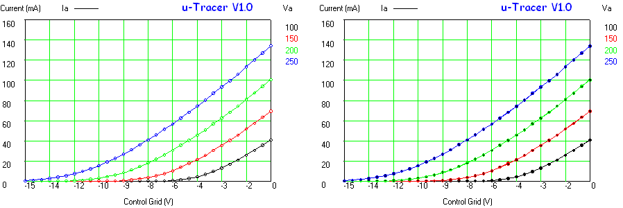
Figure 13.3 Ia(Vg) set of curves for an EL84 (left) the same measurement overlaid with a new measurement (right) showing the excellent reproducibility and absence of drift and offset (as compared to the version 2 uTracer).
Compared to the version 2 uTracer, the reproducibility of the measurements with the version 3 is excellent. Figure 13.3 (left) shows an Ia(Vg) set of curves for different anode voltages of an EL84. In the right graph in Fig. 13.3 this measurement was overlaid with a new measurement using the store and retrieve option of the GUI. As can be seen the two measurements overlay perfectly! Since the version 3 does not require stabilization cycles as in the version 2 the measurements are also much faster.
A typical measurement as shown in Fig. 13.3 takes about 25 seconds. About half of this time is spend on charging the buffer capacitor of the boost converter, giving the constraints of the design this is unfortunately unavoidable. The other half of this time is spend on discharging the buffer capacitor for the measurement of a new sweep. In retrospect the choice for a discharge resistor is not so clever. The lower the voltage, the more time it takes to discharge the capacitor. A current source would have been a much better idea. I will first finish the circuit as is, and I think I will then replace the resistive discharging for a current source discharge circuit. Anyway, 25 seconds may seem long, especially compared to some of the other tube curve-tracer designs which have been proposed, but it is the price for its simplicity and by the way, the waiting for the filament to reach its operating temperature also takes about 30-60 seconds!
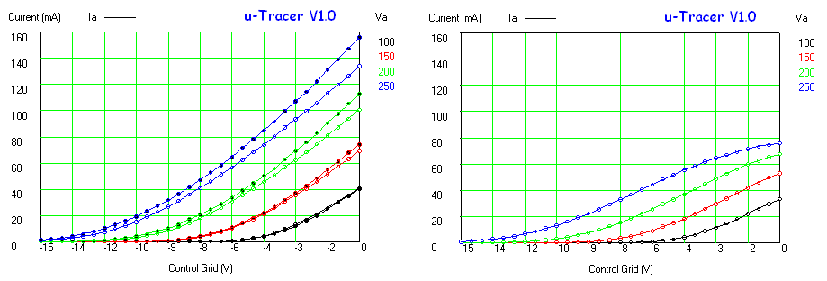
Figure 13.3 (left) variation between two EL84 which both would qualify as good, (right) an EL84 with an emission problem.
The first experience with the version 3 is that it is a pleasant instrument to work with. The measurement could have been somewhat faster, but it is not at all irritating. The store and retrieve option is especially useful in comparing tubes. Figure 13.3 shows the tube-to-tube variation between two EL84 tubes, both from Philips. I spend 15 minutes in sorting out my EL84 stock and found several bad ones which showed an emission problem especially at higher current levels (Fig. 13.3 right).
Testing Magic Eyes (for free)
Like so many other admirers of vacuum tube technology, I have “a weak spot” for Magic Eyes. I find them fascinating tubes, but then again I have a passion for every tube which in one way or the other emit light. Testing of a magic eye in the sense of taking its I-V curves usually doesn’t make much sense. The big question usually is: are the phosphors and the emission of the cathode still sufficient to produce a nice image?
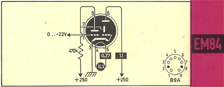 To produce the green patterns displayed by a magic eye basically a high voltage power supply, a negative grid bias supply and a filament supply are needed. We have all of those in the uTracer, but unfortunately the anode supply is pulsed so that the image will be (I guess) invisible.
Testing the boost converters it occurred to me that the boost converters obviously also can generate a useful continuous current. To get an idea of how much current the boost converters can generate a 100 k resistor was connected directly across the buffer capacitor of the boost converter. It appeared that the converter could easily generate 300 V in continuous mode which corresponds to 3 mA. With a 50 k resistor the maximum voltage reached was 250 V, corresponding to 5 mA. More than enough to drive all the magic eye tubes I know. Beautiful and so simple! We only need an additional connection to the positive terminal of the buffer capacitor and a modification of the firmware and the GUI and the uTracer can also be used “to play with” magic eye tubes. It is also possible to connect the “triode” section of the magic eye to the anode terminal and the “CRT” section to the screen terminal of the uTracer. In that way both voltages can be set independently while additionally the current can be measured. Although I do not directly see what the advantage could be, of course also “low current” normal tubes can be measured in this continuous mode.
What’s up next
Fortunately there is still enough work to be done on this project. At the moment the temporary wiring between the micro-controller and the analog electronics on the backside of the PCB is a mess that needs re-wiring in its final layout. Other changes are: reducing the value of the current sense resistors to 18 ohm, implementing the HV-on indicator and emergency stop button, adding the bandwidth reduction capacitors and replacing the discharge resistors with a current source. Also the screen supply has not been tested yet. After this the hardware will be basically ready so that I can devote my attention to upgrading the firmware and the GUI to implement: (auto) ranging, (auto) ranging, averaging, current compliance setting and measurement of the transconductance and output resistance.
| to top of page | back to homepage | to part I |
At the writing of these words the hardware of the uTracer V3 is finished and fully tested. I am happy to say that it is working better than I could have dreamed! All testing so far has been done with the V2 Graphical User Interface (GUI). This means that most of the new hardware features such as ranging and compliance setting are only accessible by modifying the firmware in the microcontroller. Nevertheless, I could not resist making a small movie which shows the basic operation of the uTracer. After some searching on the web, I found the “Free Screen Recorder,” a nice small tool which allows you to capture and record part of the screen and record spoken comments. Near the end of the movie the sound and the images are a bit out of sync, which is something I will have to look into. In the mean time I have been working hard on both the firmware in the microcontroller as well as the GUI to make the new features available in the GUI. At this moment all the features related to (auto)ranging, (auto)averaging and compliance setting have become available, and work like a dream. It was quite a bit of tricky programming, and in this section I will describe some of the details of its working, again mainly for my own documentation. I am afraid it will be quite a lengthy and boring story, but I promise that in the next section I will show some nice examples of the uTracer in action.
Setting the compliance
Rather surprisingly this section starts with a discussion on the details of the current compliance mechanism. The reason is that this part of the circuit determines the selection of the value for the current sense resistor, which is at the heart of the measurement system. It will be remembered that the uTravcer V3 has two mechanisms to protect it against over-current and short-circuit conditions. In the first place there is a very fast current limiting circuit implemented in hardware (circuit around R10 and T4 in Fig.6.5). This simple provision limits the current to ca. 250-300 mA. However, it does not protect the high-voltage switch against the excessive dissipation during a complete short circuit at high voltages. Suppose e.g. that a short circuit occurs at 350V. This would result in a dissipation of 70 W, which (as I found) is too much, even for one millisecond. For this reason the uTracer has a second over-load protection provision which is explained in Fig.5.3. In this case the voltage over the current sense resistor is (after inversion) directly fed into one of the inputs of the on-chip comparators. The other input of the comparator is connected to the on-chip programmable voltage reference. When the voltage over the current sense resistor exceeds the reference value, an interrupt is generated which immediately aborts the measurement pulse (see also text around fig.2.4). The fact that there are two on-chip comparators makes it possible to protect both the anode, as well as the screen power supplies. Since both comparators are connected to the same programmable voltage reference, the current compliance value is the same for both channels.
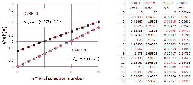
Figure 14.1 The voltages that the on-chip voltage reference can generate and the corresponding compliance current values based on a current sense resistor of 18 ohm.
The voltage reference is however a peculiar device. Basically it is a 4 bit ladder network DA converter. It can operate in two modes, determined by the value of bit CVRR. In total 32 Vref values can be generated and Fig.14.1 shows hows, depending the value of CVRR, how Vref depends on the DA converter input. The highest value the voltage reference can generate is 3.59 V. The value of the current sense resistor is selected so that this voltage corresponds to a maximum current of 200 mA, the maximum current the uTracer is designed for. Using the excel table shown in Fig.14.1 I selected the voltage reference settings which as good as possible resulted in the compliance range 200, 175, 150,…, 25 mA. The settings are stored in a table in the GUI and send to the uTracer in the “<00> settings” string which preceeds a new measurement sequence.
On top of this the user has the possibility to select the option “compliance off.” In this case the global interrupt during the measurement pulse is disabled. The use of this option is not recommended and should only be used for tubes which have already been tested at maximum voltages with the compliance on. Switching the compliance off makes it possible to extend the measurement range to 250-300 mA depending on the exact value of the current limiting resistor.
(Auto)-Ranging
The on-chip AD converter has a resolution of ten bits. In order to use this resolution to the maximum, the programmable Gain amplifiers have to be adjusted in such a way that the amplified signal uses as much of the available 0-5 V input range of the AD converter as possible. In the V3 uTracer this can be done manually or automatically. In the manual mode the user can set the gain of both the anode current amplifier as well as the screen current amplifier in such a way that it matches the currents measured. However, in this way the gain of the PGA is the same for all the measurement points in one sequence. In the automatic mode, the gain of the PGA is automatically adjusted in such a way that for every measurement point the optimal value is chosen. In most cases the automatic mode results in the most accurate measurements.
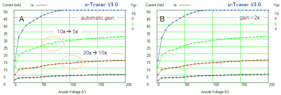
Figure 14.2 An Ia(Va) plot for Vg=-10V,-8V,-6V,-4V and Vs=200V. The left set of curves was measured using the automatic gain option. The automatic selection of another gain setting causes small discontinuities in the current. Re-measuring the set of curves with a fixed gain results in a smooth set of curves.
A small drawback is that when in automatic mode a gain change occurs in the middle of a graph, small jumps in the curves as a result of inaccuracies in the absolute gain of the PGAs can occur (Fig. 14.2A). For a perfect plot it is therefore best to first perform a measurement in automatic mode to find the proper ranges for both anode and screen currents and then to re-measure the curves using fixed (manual set) gains (Fig. 14.2B).
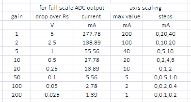
Figure 14.3 Exact ranges as a function of gain for a current sense resistor of 18 ohm.
Figure 14.3 lists, based on a sense resistor of 18 ohm, the measurement ranges for the different PGA gain settings. For e.g. a gain of 20, the voltage required at the input of the PGA for maximum ADC input (5 V) is 0.25 V. This corresponds to a current of 14.7 mA thought the 18 ohm sense resistor. The practical range associated with this gain setting in the GUI was set to 0-10 mA.
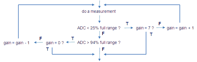
Figure 14.4 Basic automatic gain selection algorithm.
One of the most useful features of the version 3 uTracer is the auto-ranging option. When auto-ranging is used, we are assured that the most optimal PGA gain is used for every measurement point. Figure 14.4 explains the basic algorithm behind the auto-ranging feature. After each measurement the firmware in the micro-controller first checks if the measurement is larger than 94% of the maximum ADC range. If this is true, the controller tries to decrease the gain of the PGA. If the ADC result is smaller than 94% it checks if it is smaller than 24%. In that case it tries to increase the gain of the PGA. If the measurement result is in between 24% and 94% of the total ADC range, it assumes that the current gain setting is optimal. After each gain correction the measurement point is re-measured until the optimal gain setting is reached. It can be that the gain cannot be increased or decreased any further, in that case the iteration process is also terminated.
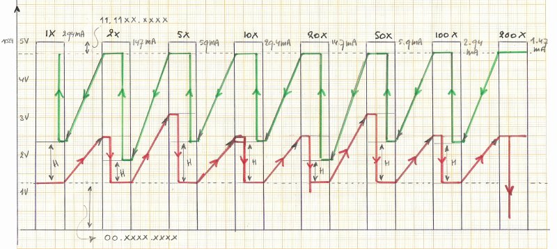
Figure 14.5 Graphic illustration of the automatic gain hopping algorithm (see text below).
The automatic gain selection (gain hopping) process is graphically illustrated in Fig. 14.5. Every time the ADC input becomes less than 1.25 V the gain is increased, resulting in the red line which runs from left to right. When the input voltage increases beyond ca. 4.7 V, the gain is decreased resulting in the green curve running from right to left. Note that the input voltage margin denoted by H (Hysteresis) is the margin which prevents a fast hopping between gain settings in case of a noisy signal. In reality the situation is a bit more complex due to the fact that both the PGA for the anode current as well as the PGA for the screen current have to be set using the same measurement. In the final implementation also a counter was added which limits the number of iteration cycles to 8 so that the algorithm will always terminate. A description of the complete algorithm is given below.
Figure 14.5 also explains the selection of the threshold values of 24% and 94%. These values are selected to make the detection of a therhold crossing as easy as possible. Of course it would have been possible to implement this using a two byte full numeric comparison, but that would have required quite a bit of hustling with variables. The way it is implemented here is very straightforward. When the higher byte of the ADC result is zero, the result is below 25% of the maximum ADC range. When the lowest two bits of the high-byte AND the highest two bits of the low-byte are all 1, the result is larger than 94%:
The program flow for a single measurement
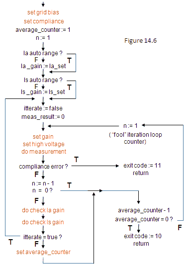 The whole measurement sequence, including auto-ranging and averaging is controlled by an assembler routine which, appropriately, is called “do_10.” The working of this routine is not very complicated, but tricky enough to spend a few words on it. Figure 14.6 shows the schematic flow diagram for the measurement routine. The routine first starts by calling two other routines (sub-routines are colored red) which set the grid-bias and the compliance; they are pretty straightforward. Next a counter which is used to counts down the number of measurements during an averaging sequence is initialized to a default value of 1. The counter is set to its final value later on. The reason for this is that when the user has selected both the auto-gain as well as the auto-averaging option, the exact number of iterations can only be set once the gains have been established. Finally counter “n” which keeps track of the total number of iterations is initialized to 8.
Before a new measurement sequence is started, the actual gains (Ia_gain, Is_gain) are set to 100X. This is done during the execution of the routine which executes the settings <00> string which precedes a new measurement sequence. The gain of 100X is the default starting gain used in the automatic gain algorithm. A rather high gain is used as starting value, because most curves begin at low currents. Note that for any next point in a measurement sequence, the gain setting found for the previous point is used, to reduce the iteration time. If however manual settings for the gain are used, the actual gains are set to the specified gains (see flow diagram).
Next the iteration loop is started. First a bit of explanation on the averaging process is needed. What is important to know is that the AD-conversion routine which measures the anode and screen currents not simply stores the ADC result in the output variable (called “meas” in the flow diagram), but adds the result to the output variable. So after N calls to the AD-conversion routine, we only have to divide the result by n to get the average. This is the reason why “meas” is set to zero at the beginning of the iteration loop. The iteration process is controlled by flag “iterate.” When either the anode current or the screen current are out of range, the iterate flag is set, resulting in a new iteration. Since in this way both the anode, as well as the screen current gains are optimized at the same time, the number of measurements, and thus the iteration time is minimized.
Finally, the first measurement is performed. First the actual gain values are programmed into the PGAs (“set gain”) and the high voltage capacitors are charged to the specified voltages (“set HV”). Routine “measurement” switches off all the boost converters and the filament driver, issues the actual measurement pulse and calls the appropriate AD-conversion routines to measure the anode and screen currents. A compliance error will directly terminate the measurement. After each measurement, the maximum iteration counter n is decremented. When it reaches zero, the iteration process is aborted and the last gain settings are used. When n is not yet zero, two routines are called which check if the anode current and the screen currents are within range. When either the anode, or the screen current are not yet within range, the routines set the “iterate” flag, and increment or decrement the gain. If the “iterate” flag remains cleared, the iteration process is complete and the final values for the gain are found. The averaging cycle is now started.
Also the averaging process is optimized for speed, or in other words as little of measurements as possible. To achieve this also the last measurement which was used in the iteration process is used for the averaging. It should be realized that most of the measurement point are “within range,” while for most ranges no averaging is required. So for the majority of measurement points only one measurement is needed! When averaging is required (averaging counter <> 0) a new measurement is performed. A trick is used “to fool” the iteration loop: by setting n:=1, the iteration loop exits before the ranges are checked. Not really very transparent, but reasonably elegant and certainly compact. When the average counter reaches zero, the measurement of this particular point is completed.
Automatic Averaging
Already quite a lot has been said about the averaging. Like the gain, also the averaging can be set manually to multiples of 2 (off, 2X, 4X, 8X, 16X or 32X) or the user can select the automatic averaging option. In this mode the number of averaging measurements is automatically selected based on the gain. Since the anode and screen currents are measured at the same time, the algorithm determines MAX(Ia_gain,Is_gain). Based on the maximum gain a small look-up table is used to find the number of measurements. So when both the gains, as well as the averaging are set to automatic, we are assured of the best selection of measurements conditions for every point in the curve. The number of average measurements as a function of maximum gain is listed in Fig. 14.7.
Figure 14.7 Number of average measurements used as a function of maximum gain in “auto-averaging mode.”
After the micro-controller has found the optimal gains - and thus the required number of average measurements - only the gains are reported back to the GUI and not the number of average measurements. The reason is that this again would have required an extension of the report string. Still the GUI needs the number of average measurements used because the floating point division is done by the GUI. To find the number of measurements the
GUI uses exactly the same algorithm as the firmware in the micro-controller. From the maximum gain the number of measurements is found using a look-up table. So if for one reason or the other the look-up table has to be changed, it has to be changed both in the firmware as well as in the GUI.
Setting the high voltages
 The direct control of the boost converters is done by the interrupt service routine as explained in section 4 and ,in section11. However, the discharging which is necessary to discharge the capacitor when the starting voltage is too high is implemented in routine “set_HV.” This routine additionally takes care of the 10 ms discharge pulse which charges the high-voltage switch “battery capacitor.” The “set_HV” routine is executed immediately before the actual measurement routine.
Figure 14.8 shows the schematic flow-diagram of the “set-HV” routine. First the 10 ms discharge pulse is issued regardless of the state of the reservoir capacitors. Both the anode and screen converters are switched off, and the discharge outputs are made high, followed by a delay of 10 ms. This simple piece of code gave me quite some headache. The problem was that the interrupt routine which is running on the background continuously switches off the discharge outputs!. The solution was to continuously set the discharge outputs in the 10 ms delay loop. In that way the discharge is continuously being set during the delay.
Next both reservoir capacitors need to be discharged to some voltage below the set-point. The information on whether the reservoir capacitor voltages are higher or lower than the respective set-points is obtained from the interrupt service routine. As explained in section 11, the interrupt service routine is continuously comparing the reservoir capacitor voltages to the set-points, even if the boost converters are disabled. If the respective mask bit is high, the voltage of that boost converter as dropped below the set-point. This information is used by the “set-HV” routine, even though the boost converters are switched off.
To explain the working let’s take the anode boost converter as an example. As soon as the Anode_BST_MSK bit becomes true, the discharge output is made low. Additionally the Anode_BST_OK flag is made low to indicate that the voltage on the anode reservoir capacitor is not valid yet. Finally the anode boost converter is switched on by setting Anode_BST_ENBL. If the Anode_BST_MSK bit was not high yet, we keep on making the discharge output high because the interrupt service routine keeps on resetting it. In this way the Anode_BST_ENBL bit works as a flag which when set signals that the discharge cycle is complete and that the boost converter is running.
The same principle is applied to the screen boost converter. As can be seen from Fig. 14.8 both boost converters are serviced in a loop so that they are serviced simultaneously. The condition to exit the loop is that both the Anode_BST_ENBL and the Screen_BST_ENBL bits are high (indicating that the discharge loop has been completed, and that the information in the OK bits is valid) AND that the Anode_BST_OK and the Screen_BST_OK bits are high (indicating that the voltages on the boost converter reservoir capacitors have reached their set-point values and are being serviced to keep that voltage.
Control of the “High Voltage On” LED.
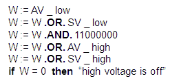 The “high voltage on LED” is on when there is a high voltage present on either of the two buffer capacitors. The LED is directly controlled by the interrupt service routine. It will be recalled that the interrupt service routine continuously measures the voltages of both the high voltage reservoir capacitors and the negative power supply capacitor.
A straightforward way to implement this function would have been to compare the 2-byte AD-converter results for the anode as well as the screen with some threshold value and then to switch the LED on when either of the voltages exceeds the threshold. This is however rather cumbersome and boring so a faster and cleverer algorithm was used.
The “high voltage on LED” is on when there is a high voltage present on either of the two buffer capacitors. The LED is directly controlled by the interrupt service routine. It will be recalled that the interrupt service routine continuously measures the voltages of both the high voltage reservoir capacitors and the negative power supply capacitor.
A straightforward way to implement this function would have been to compare the 2-byte AD-converter results for the anode as well as the screen with some threshold value and then to switch the LED on when either of the voltages exceeds the threshold. This is however rather cumbersome and boring so a faster and cleverer algorithm was used.
It is straightforward to show that ADC result 1111000000 corresponds to slightly more than 22 V. In other words when the ADC result is 0000XXXXXX (X = don’t care) the voltage is below 22 V. The only thing we have to do then is to check for both the anode as well as the screen if these four bits are zero. A slight complication is that the four bits are stored in two variables. The highest two bits are stored in AV_high (in case of the anode voltage) while the other two bits are the highest two bits in AV_low.
The short piece of code to the left illustrates how this check can be implemented in assembler. First the “low bytes” of both the anode and the screen voltages are “ORed” into the working register. “AND”ing the result with 11000000 will make the lower order 6-bits zero. The working register is now zero if the highest two bits of both voltages are zero. Next the “high-bytes” of the anode and screen voltages are “ORed” into the working register. A “1” in either of the two “high-bytes” will make the working register “non-zero.” Only six instructions = 1.4 us!
| to top of page | back to homepage | to part I |
The command and result strings.
The communication with the uTracer is via a serial RS232 link at a speed of 9600 baud, 8 bits, no parity, and one stop bit. The commands to the uTracer are given in the form of a string of 28 (Uppercase) ASCII characters. Each character sent to the uTracer is immediately echoed. Failure to echo a character represents a malfunction of the uTracer.
Every two consecutive characters in the ASCII string represent an eight bit byte. The first byte is the command code. The following 8 bytes represent data. Different formats for the data are used depending on the command code, however in most cases the eight bytes are grouped into four 16 bit words representing the anode voltage, the screen voltage, the grid voltage and the filament voltage.
Some strings do not result in a response from the uTracer. Other strings result in the uTracer sending a result string. The result string also has a fixed format, and consists of 38 ASCII characters. Again every two consecutive characters in the ASCII string represent an eight bit byte.
The first byte is the status byte which signals if the command to which the result string was a response was executed successfully. The remaining 18 bytes represent data grouped into 9 two byte words. The format of the result string is fixed (Fig. 15.2).
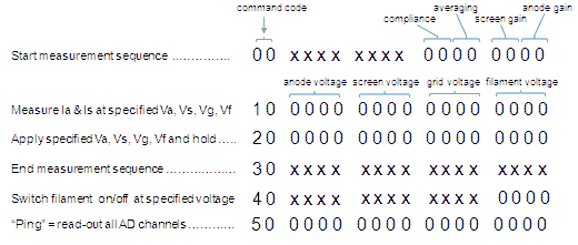
Figure 15.1 Definition of the Command Strings.
The data in both the command string as well as in the result string is always in 10 bits binary format. This means that the upper 6 bits of the data word are not used. These bits should be zero. In most cases the binary data directly represents a 10 bit result of the on-chip AD converter, or a setting of the 10 bit on-chip PWM modulator. All conversion of for the user meaningful numbers to and fro binary representations is done in the GUI. In this way a minimum amount of intelligence is needed in the micro-controller.
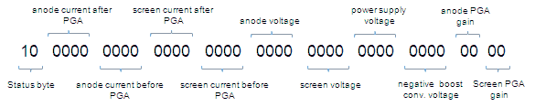
Figure 15.2 Structure of the Result String
Structure of a complete measurement sequence
The different commands should be send in a certain order, although sending the commands in a random will not result in an error. The preferred command sequence is shown in Fig. 15.3. When the “Heater On” command is pressed, the GUI send a “Set Settings” (<00>) command followed by a “Ping” (<50>) command to obtain the current supply voltage. It then sends “Switch On Heater” (<40>) command. The only thing this command does is to copy the last word of this command to the filament PWM generator. The other words should be “0000”. The filament
voltage can be directly set to the final value or the GUI can generate a “soft-startup” by issuing a sequence of <40> commands with increasing filament voltage values. The uTracer does not send a response after receiving a <40> command
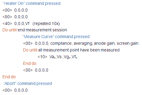
Figure 15.3 Structure of a typical Measurement Session
While the filament is heating, the user has the time to select a measurement type on the GUI and to set the proper measurement conditions. When next the user presses the “Measure Curve” button, the sequence to measure a set of curves is started. The first command issued is the <00> “Send Settings” command. This command transfers the gain settings for the anode and screen amplifiers, the required number of average measurements and the current compliance value. There is no response of the uTracer to the <00> command. Next the GUI starts issuing <10> “Do Measurement” commands. The four words in the command exactly specify the anode, screen, grid and filament voltages. After reception of the command the uTracer sets all the specified bias conditions and performs the measurement. The result is communicated back to the utracer in a result string. The value of the status byte indicates if the measurement was successful. If the status byte = 10H everything is ok, a value of 11H indicates a compliance issue on one of the two channels. The GUI can issue any number of <10> commands. At the end of a measurement sequence the GUI issues the <30> “End Measurement” command. This command discharges the high voltage buffer capacitors and set the grid voltage to zero. In the same measurement session more curves or a different type of curve can be measured by repeating the <00>,<10><10><10>….,<30> sequence. At the end of the session the filament voltage is switched off by issuing a <40> command with a specified filament of zero volt.
The format of the variables
In this section the format of the variables that are used in the communication with the uTracer will be defined. Some of these variables are one byte, while other variables use two bytes (a word).
anode and screen gain
The anode and screen gain variable is only one byte long, and used both in the <00> command string, as well as in the result string. In the command string it is used to specify the gain of the anode or screen current amplifiers, or to specify that the “auto gain/range” option is selected. In the return string the variable returns the actual gain as it was determined by the “auto range” algorithm in the uTracer and used for the current measurement point. The lower nibble directly reflects the gain convention as it is used by the PGA113: 00H=1X, 01H=2X, 02H=5X, 03H=10X, 04H=20X, 05H=50X, 06H=100X, 07H=200X. In addition code 08H is used to indicate that the auto-gain algorithm has to be used.
averaging
The average variable is one byte long. The variable is only used in the <00> command string. In principle the variable can have any value in between 1 and 32 (001H and 20H). In practice only the values 1, 2, 4, 8, 16 and 32 are used. This is because the user can only choose from these values. When the variable has the value 40H it indicates that the auto-averaging algorithm has to be used
compliance
The compliance variable is one byte long and only used in the <00> string. The variable defines the voltage of the on-chip voltage reference which is compared by the two on-chip comparators to the voltage drop over the current sense resistors. When the voltage drop over the resistor exceeds the reference voltage, the measurement is aborted. The value of the compliance variable is directly copied into the CPU register which controls the voltage reference: CVRCON.
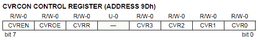
Since the voltage reference has to be enabled (CVREN=1) and disconnected from the output pins (CVROE=0) the highest two bits of the variable have to be always 10xxxxxx. VCRR defines the measurement range while the lowest nibble of the variable selects the tap in the resistive ladder network. When the variable has for example the value 10001111=8FH a 200 mA compliance has been selected (see also section 14).
anode and screen voltages
The term anode and screen voltages in the context of the variable description is rather misleading since the variables not so much specify the anode and screen voltages itself but rather the voltages of the anode and screen buffer capacitors. It will be recalled that the cathode of the tube is referenced to the power-supply voltage of 18.5 volt so that there is also an offset of 18.5 V between the voltage of the buffer capacitor and e.g. the anode voltage. To be more precise the anode (screen) voltage is the voltage of the anode (screen) buffer capacitor minus 18.5 V. The voltage of the buffer capacitor is measured using a resistive voltage divider so that a 0-350 V range is mapped on a 0-5 V range. The conversion formulas which give the relation between variable n and the high voltage(s) are:
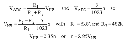
The anode and screen voltages variables occupy two words and are used both in the command as well as in the result string. Since a 10 bit AD converter is used, only the lower 10 bits of the two bytes are used. The variable n in these equations can have any value between 0 and 1023 (358 V).
anode and screen currents
The anode and screen currents are measured from the voltage drop they cause over a current sense resistor of 18 ohm. If desired the voltage drop is first amplified by a Programmable Gain Amplifier (PGA) before being fed into the AD converter. When an averaging larger than 1X is used, the uTracer just adds the measurements to the variable which is transferred to the GUI. The GUI subsequently performs the floating point division. The relation between the variable n, and the anode/screen currents (in Amps) is given by:
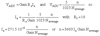
The anode and screen current variables occupy two words and are only used in the result string. Although only a 10 bit AD converter is used, the variable can use the full two byte word of 16 bits for 32X averages. Two values which are also returned are the anode and screen currents before the PGA. In other words the voltage directly over the current sense resistors (after inversion). This value is not used by the GUI. The conversion formulas are identical to the equations above with Gain=1 and Average=1.
power supply voltage
The power supply voltage is measured because it is an important parameter in the calculation of the settings for the proper filament voltage. It is only used in the return string. Like the high voltages, the power supply voltage is simply measured using a simple resistive voltage divider consisting of R43 and R44 (Fig. 13.1). The values for R43 and R44 are chosen such that a power supply voltage range of 0-23.9 V are mapped on the ADC input range of 0-5 V.
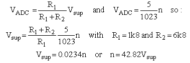
control grid voltage
The control grid variable sets the control grid bias. The control grid voltage is always negative with respect to the cathode which is at the same potential as the unregulated supply voltage (see section 2). The control grid bias circuit is driven by the output voltage of the 10 bit on-chip PWM generator. Although the control grid voltage variable is 2 bytes wide (16 bits), only the lower 10 bits are used to directly program the PWM generator. The relation between the variable n and the grid bias is given by (section 7):
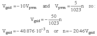
filament voltage
Also the filament voltage is controlled by a 16 bit word which is only used in the command string. The word is directly used to program one of the on-chip PWM circuits. The PWM circuit is set at a repetition frequency of 19.5 kHz, when the variable is zero the duty cycle is also zero and the filament voltage is zero. When the variable is 03FFH, the duty cycle is 100% resulting in a filament voltage equal to the supply voltage. There is a quadratic relation between the effective filament voltage and the duty-cycle (d). The relation between the variable (n) and the filament voltage is given by:
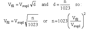
negative boost converter voltage
The negative boost converter voltage is not a variable which is set by the GUI, but rather it is specified during the initialization of the firmware to a fixed value of -40 V. The relation between the variable (n) and the negative boost converter voltage (Vboost < 0) is given by:
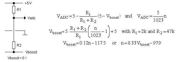
| to top of page | back to homepage | to part I |
Although I still want to add a number of features such as auto scaling and transconductance plotting to the GUI, all essential components are now in place and it has become time to do some real testing! It is my plan to test a number of devices in this section and to see how well the uTracer is behaving and what there still is to improve.
After writing the previous lines, a number of weeks have passed spent on measuring all kind of tubes. I am delighted to say that the uTracer is behaving exactly, or even better, than I expected. Especially the auto-gain and auto-averaging options make working with the instrument a pleasure, because you basically never have to worry about these settings. It was so much fun that this has become a rather long section so that I have added in index below. Of course there are still some things to be improved of changed and I will discuss those at the end of this section.
|
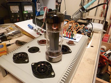
|
Resistors
Throughout the debugging of the hardware and the software I have used a pair of resistors as DUT (Device Under Test) instead of a tube. The reason is that resistors have no filament which needs heating and have a very simple and predictable behavior. I especially made a switch box with two sets of four 0.1 % resistors with values 1M, 100k, 10k, 1k, one set for the anode and one set for the screen.
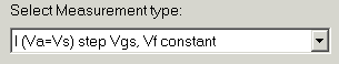 To measure the resistors the “I(Va=Vs)” measurement type is used. In this measurements the anode voltage and the screen voltage are both equal and also the “sweeping variable” while the grid voltage is stepped. Obviously the grid is not connected during this measurement so only one grid bias is used. This measurement type is also very useful for pairing double diodes/triodes.
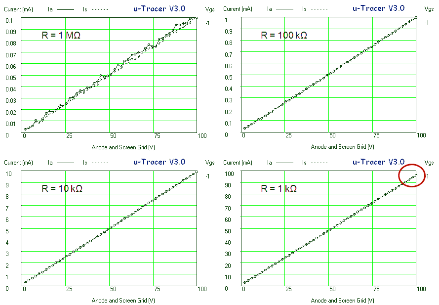
Figure 16.1 I-V curves of two equal resistors connected between the anode and screen terminals and the cathode terminal.
Figure 16.1 shows a set of four resistor measurements. Each time two identical 0.1% resistors were connected between the anode and screen connections and the cathode connection. The anode and screen gains, as well as the averaging controls were set to automatic. Except for the most sensitive range the measurements are very nicely linear and practically offset free. Both the screen and the anode current practically coincide, as they should. The gain of the whole system was adjusted by tweaking the value of the current sense resistor in the GUI software. With the original default value of 17.3 ohm, the current at 100 V was slightly too high (1.03 mA for 100 kohm). By adjusting the resistance value in the GUI software to 17.8 ohm, the current at 100 V was exactly 1 mA. Also for the 1 M and 10 k load resistors the Gain was now ok.
For the 1 kohm resistor (0 – 100 mA range) the measured current appears to be too low. What is happening here is something different. What has not been taken into account yet in the GUI is the voltage drop during the measurement over the current sense resistor and the high voltage switch while also the discharging of the buffer capacitor has been neglected so far. So in reality the measurement voltage is a bit lower than the set point voltage. The deviation becomes larger for higher currents. Fortunately all the voltage drops are known, and correcting for it is something still on my list of things to do.
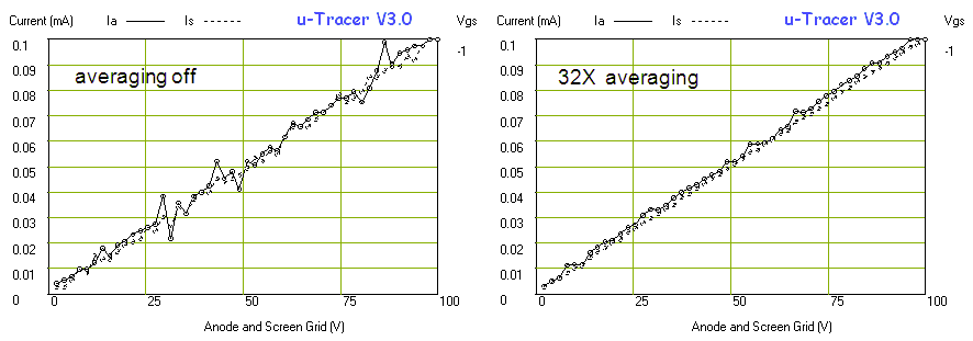
Figure 16.2 I-V curves of two 1M resistors connected between the anode and screen terminals and one of the filament terminals with averaging off and 32X
For the most sensitive 0 - 100 uA range the signal is rather noisy. The strange thing is that for one reason or the other the screen current is less noisy than the anode current. The noise becomes even more pronounced when the averaging is switched off. In the auto-averaging mode the uTracer set the averaging to 8X for the highest sensitivity range. In Fig. 16.2 the averaging was first switched off (left) and then set to 32X (right). At the moment I have no idea of the cause of this difference between the anode and the screen channels. It is certainly on my list of things to sort out. Since the screen current is ok, it is probably a problem in one of the components, or a layout related issue. It at least shows that it is possible to measure down to the 10’s of microAmp range with this very simple circuit.
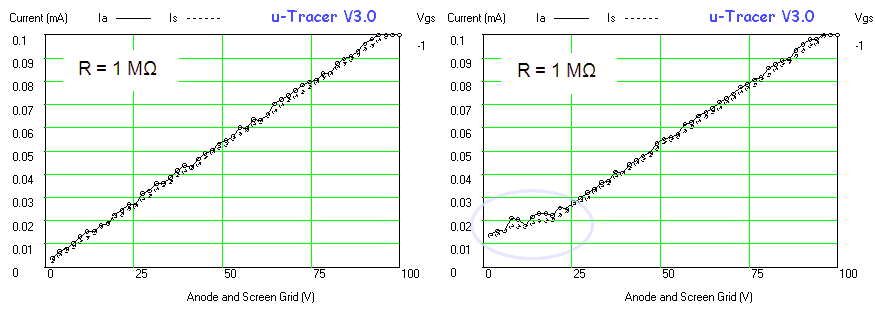
Figure 16.3 I-V curves of two 0.1% 1M resistors connected between the anode and screen terminals and one of the filament terminals.
Another interesting thing to test was the simple trick that was implemented to allow testing of directly heated cathodes. So whereas in the previous two measurements the resistors were “grounded” to the cathode connection, this time they were connected to the filament connections. In the graph of Fig. 16.3 they were connected to the “hot-side” (= the MOSFET switch) while in the left graph they were connected to the other filament connection. For the higher current ranges everything works like a charm, only for the lowest current range we find a tiny leakage current of ca. 20 uA. It will be remembered that the filament bias is completely switched of during the measurement pulse. However, the only path for a leakage current can be through the MOSFET.
This means that either the MOSFET is leaky, or that the time between switching it off and the MOSFET indeed being fully closed is too short. Insertion of a small delay in the firmware will sort that out. Although we can easily live with the leakage current it is worth looking into.
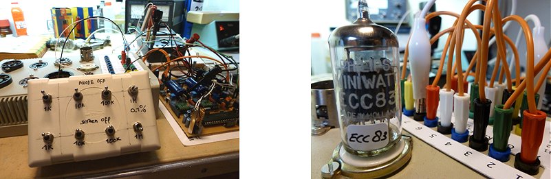
ECC83 Double Triode
The ECC83, or the 12AX7 as it also known, is a much loved tube amongst vacuum tube audiophiles. It was developed around 1948 by R.C.A. and subsequently copied and perfected by Philips-Mullard in Europe. The tube has a very high amplification (mu > 100) mainly as a result of its high output impedance. With its low bias current of 1.2 mA the tube is mainly used in resistor coupled pre-amplifiers and phase-splitters
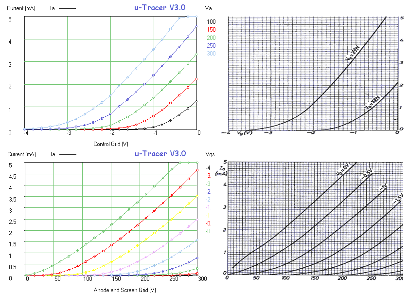
Figure 16.4 Ia(Vg) and Ia(Va) curves of an ECC83 (12AX7) compared to the curves in the original datasheet (Source: Franks Tube Data).
In Fig. 16.4 both the Ia(Vg) curves as well as the output curves are compared to the original datasheet. Note that my ECC83 draws a bit less current than the current specified in the datasheet. From these measurements it is clear to me that the next important addition to the GUI will be the measurement of the transconductance and the output resistance and thus the amplification. However, I still haven’t made up my mind how to do that exactly. Directly differentiating the Ia(Vg) and Ia(Va) curves can result in a mess when these measurements are a bit noise. What I plan to do is first fit a polynomial to the curves and then to differentiate them numerically.
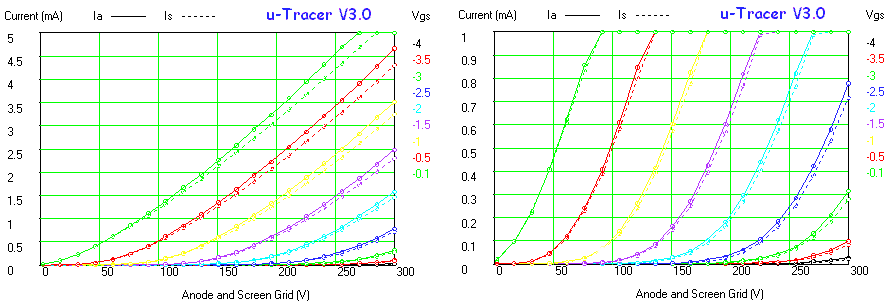
Figure 16.5 Left: output curves for each of the sections of the ECC83. Right: same measurement but then at 0-1 mA scale.
One of the nice features of the uTracer is that it is possible to measure both sections of the double triode simultaneously by simply connecting the anode of the second section to the screen connection on the uTracer. Using a special measurement type (see section of resistor measurement above) both Va and Vs are swept simultaneously. The left graph of Fig 16.5 shows a comparison of the output characteristics of both sections of a single ECC83. As can be seen there is a small difference between the sections. I have no idea if this difference is significant for high-quality audio amplifiers. One of the nice things of the auto-ranging option is that all measurement point are taken with the same accuracy. It is therefore directly possible to zoom in on the measurement as shown in the right graph of Fig. 16.5 where using the same set of measurement point the current scale as been magnified to 0-1 mA.
The ECL80
The ECL80 is one of the first triode/pentode combinations in a noval base designed in the early fifties probably by the tube development of Bert Dammers of the tube lab of Philips at the Emmasingel in Eindhoven, the Netherlands (more info here). The tube is a bit special because it was used as an example in the paper by Dammers on one of the first tube curve-tracers in the Philips Technical Review. The ECL80 was primarily designed for use in television receivers with the triode as a frame blocking oscillator and the pentode as a frame output amplifier (more info here). Next to this, the tube was also used in a (low-cost) audio applications.
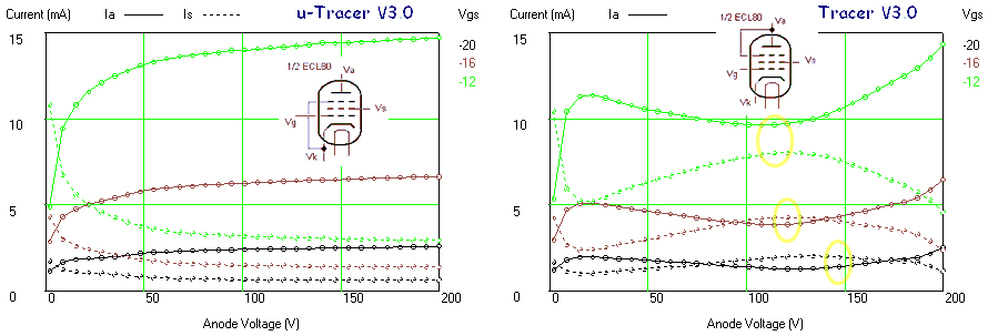
Figure 16.6 ECL80 in pentode- (left) and tetrode mode (right). The screen voltage was 220V in both cases.
Unlike many other pentodes, the suppressor grid of pentode section of the ECL80 is not internally connected to the cathode, but accessible though one of the pins. This makes it possible to use this section as a normal pentode by connecting the suppressor grid externally to the cathode, or as a tetrode by connecting it to anode. The left graph in Fig. 16.6 shows a measurement of the ECL80 connected in pentode mode with the suppressor grid connected to the cathode. The tube has been biased a little bit below its normal bias point (Ia=17.5 mA) because in tetrode mode the kink is somewhat more pronounced for low bias values. Both the anode current and the screen current show the familiar pentode behavior. Note that for low anode voltages the screen grid takes over the role of electron collector resulting in an increase in screen current. In the right graph of Fig. 16.6 the suppressor grid has been tied to the anode so that the tube operates in tetrode mode. The anode current now shows the characteristic tetrode kink. The secondary emission electrons are collected by the screen grid, resulting in an increase in screen grid current, and a decrease in anode current. The anode and screen current shown an almost complementary behavior.
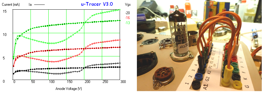
Figure 16.7 The anode current of the ECL80 in pentode mode compared to the anode current in tetrode mode (Vs = 220 V).
Figure 16.7 shows the anode current in pentode and tetrode mode plotted in the same graph. For low anode voltages, the energy of the primary electrons is low so that only few secondary electrons are generated. The anode currents in pentode and tetrode mode now almost coincide. When the anode voltage increases, secondary electrons are generated at the cathode. These electrons are attracted by the highly positive screen grid resulting in an increase of screen grid current and a decrease in anode current. When the anode voltage is increased any further, the screen grid becomes less positive with respect to the anode so that more electrons return to the anode. Now a second effect starts to play a role: the emission of secondary electrons from the screen grid. So far these electrons returned to the screen grid, however, for anode voltages higher than the screen bias these electrons are drawn towards the anode resulting in an increase in anode current to a value higher than in pentode mode. The movie below shows how these measurements were recorded. It is best viewed in full screen mode.
The VT-185/3D6, a directly heated beam pentode
The VT-185 is a nice little directly heated beam tetrode that was developed just before or in the war as a general purpose tube for portable radio equipment. It can deliver up to 2 Watt at 20 MHz or 0.5 Watt at 200 MHz, but it was also commonly used as an audio amplifier. As said it has a directly heated cathode which consists of two 1.4 V / 300 mA filaments which can be switched either in series or in parallel. After the war it was sold under the civilian tube number 3D6. It was amongst others manufactures by Sylvania and Tung Sol. I was lucky to get a hand full of them from “Radio Service Twente” in the Hague (Holland) who sells them for as little as 50 (euro) cents. Really its only drawback is that it comes in a loctal base.
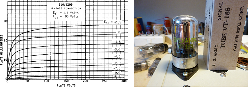
Figure 16.8 Output curve from the original datasheet from Tung-sol that was signed of June 1949
There is really not so much interesting to tell about the 3D6 apart from the fact that it nicely demonstrates that also directly heated cathodes can be tested with the uTracer V3. In the sets of output curves shown in Fig. 16.9 I didn’t use the internal filament supply, but used an external 1.5 V battery. Notice that it can make quite a difference what the polarity of the filament battery is! When the battery is connected as in the right graph, part of the filament is biased below the reference potential effectively increasing the grid bias resulting in a higher anode current. I also tested the tube with the internal filament supply. In that case I used the filaments in series. The output curves in that case were almost identical to those in the left graph of Fig. 16.9 because the filament supply is off during the measurement pulse.
Figure 16.9 Output curves of the VT-185 for the two filament battery polarities.
Diodes: AZ1, EZ81, EAA91
So far I neglected the effect that the anode and screen currents have on the anode and screen voltages. There are three effects: in the first place there is the voltage drop over the current sense resistor. In the second place the currents discharge the buffer capacitors, and finally there is the voltage drop over the high voltage switch. All these three effects lower the effective anode and screen voltages. Fortunately the three voltages drop can easily be measured or calculated (Fig. 16.10). The voltage drop over the sense resistor simply equals the measured current times the resistance of the sense resistor. The approximate voltage of the buffer capacitor at the moment of the current measurement is also known because the voltage of the buffer capacitors is measured immediately after the measurement pulse. The voltage over the high voltage switch is approximately constant (0.7 V).
Figure 16.10 I(V) curve of a 100 ohm resistor showing the impact of the anode/screen voltage correction for low voltages.
So far I have neglected these effects and just plotted the currents versus the set-point voltages. The error is usually very small; for most tubes the currents are rather small, while the voltages are high. However there is at least one type of tubes for which the error can be rather large: diodes! Evidently diodes are designed to conduct high currents with a low voltage drop over the diode. The voltage drops over the sense resistor, switch and buffer capacitor can in this case be very significant.
Figure 16.10 shows two I(V) measurements of a 100 ohm resistor connected between anode and cathode connections of the uTracer, with and without correction of the measurement voltage. Note the large difference between the curves! Both lines appear to be less “smooth” than the normal uTracer curves. There are a number of factors involved here. First we have to realize that we are at the limits of the AD converter. With a 10 bit AD converter sized for a 380 V range the voltage step per bit is ca. 0.4 V. Looking at the “uncorrected curve” we can observe small jumps in the line about every 4 measurement points. Clearly aliasing effect related to the AD converter. The “corrected curve” obviously also suffers from the limitations of the AD converter, but additionally a correction voltage, which in itself also contains an error, is subtracted from the set-point voltage resulting in a rather ragged curve. Although the curves certainly wouldn’t make it in a beauty contest they are certainly still very acceptable and at least good enough for me.
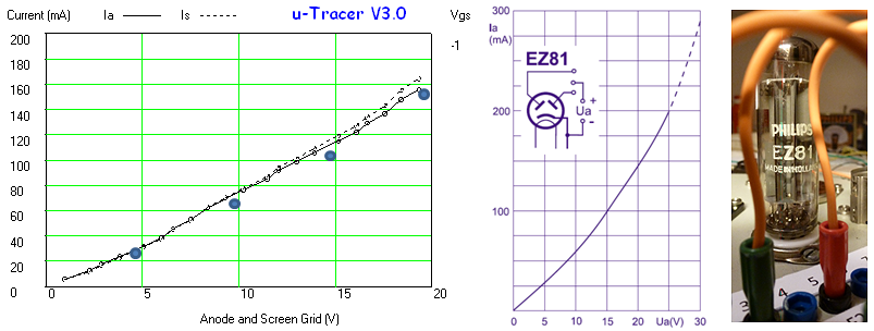
Figure 16.11 EZ81 full-wave power rectifier tested and compared to datasheet.
In Fig. 16.11 the I(V) curve of the diodes of a single EZ81 are compared to the curve from one of the datasheets. Like in the measurement of double triodes, one of the anodes is connected to the anode connection of the uTracer, while the other anode is connected to the screen connection. In this way both measurements can be compared in one measurement.
Figure 16.12 AZ1 “under test” and I(V) curve from datasheet
The AZ1 is a full-wave rectifier, double diode, that was introduced by Philips / Mullard in 1938. It uses the side-contacted ct8 base which was introduced by Philips, but never became a but success. It has a directly heated cathode using 4 V at 1 A. Figure 16.12 shows he AZ1 “undertest” and the original I(V) curve from the datasheet clipped to 200 mA.
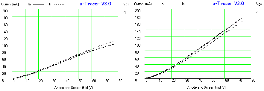
Figure 16.13 Two AZ1 rectifier double diodes compared.
I have a bunch of AZ1 and tested them all. Again the coupled I(Va=Vs) type measurement was used to measure both diodes at the same time. There was quite some variation in the I(V) curves. The tube in the right graph of Fig. 16.13 compares very well with the datasheet, producing 150 mA at 60 V drop. It is almost unbelievable how robust these guys where able to make those tubes almost 75 years ago so that they not only have survived, but actually function “as good as new.” The tube in the left graph is obviously a bit worn-out showing significantly less emission. In both cases the matching between the sections is very reasonable.
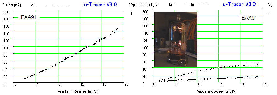
Figure 16.14 A good EAA91 (left) and a very bad one (right)
The EAA91 is a double diode with completely separated sections (two cathodes) intended for AM/FM/video detection which was introduced in 1951. It is a tiny tube on a 7-pin miniature B7G base. The length of the tube is only 36 mm (diameter 18 mm). A few years ago, Elector published a crystal-set receiver using the EAA91 as detector. I have tested a bunch of EAA91. Quite a number of them have a poor emission. Figure 16.14 shows a perfect sample (left) and a very poor one (right).
The EF50 saga
The EF50 is a landmark tube. Before the EF50 most tubes were made using the stem based technology that was also used to manufacture incandescent lamps. This technology was not particularly suitable for the fabrication of high frequency tubes. Although several tube envelopes had been proposed that were more suitable for RF operation, they all turned out to be too expensive, or not suitable for mass-fabrication. Finally the researchers at Philips succeeded in making an envelope based on a pressed glass base, which combined very good high frequency properties with low-cost, high volume manufacturability. The first tube made in this technology was the EF50. As it happened to be, this tube turned out to play an important role in WWII.
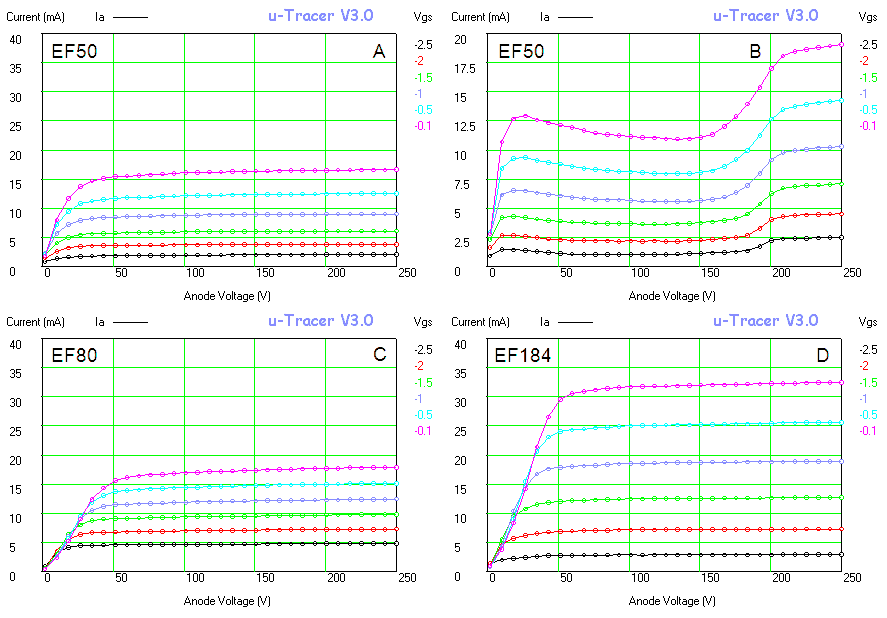
Figure 16.15 a,c,d: Ia(Va) curves of the EF50, EF80 and EF184 family in pentode configuration, and b: the EF50 in tetrode configuration.
Having researched the history of the EF50 in such depth, it is not surprising that it is a very special tube to me. I actually have several samples of the EF50 from different manufacturers and it was really a special moment to bring them to live using the uTracer. Like the AZ1 in the previous section the EF50 had survived the past 60 years without the slightest problem. Figure 16.15a shows the Ia(Va) curves of one of my EF50’s connected in pentode configuration (suppressor grid connected to cathode). In Fig. 16.15b the same measurement on the same tube is shown, but this time the tube is connected in tetrode configuration (suppressor grid connected to anode). Both the anode, as well as the screen-grid produce a significant amount of secondary electrons.
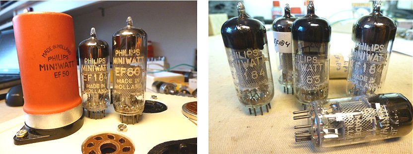
Figure 16.16 The EF50 and its children.
After the war, in 1950, the EF50 was succeeded by the EF80, this time in the NATO standard “noval” envelop. The EF80 was produced in enormous numbers. Most TV’s in the fifties were full of EF80’s performing a verity of functions: RF, intermediate frequency and video amplification. Like the EF50 all grids of the EF80 were accessible for optimum freedom of circuit design. In the sixties, the EF80 in turn was succeeded by the EF184. In Figure 16.16a,c,d the Ia(Va) curves of the EF50, EF80 and EF184 are compared. As can be seen, the mutual conductance of the EF50 and EF80 is more or less the same ca: 7.4 ma/V. From the larger distance between two consecutive sweeps in the Ia(Va) curves of the EF184 we see that the mutal conductance of the EF184 has been significantly increased (to ca. 15 mA/V).
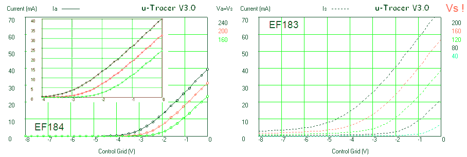
Figure 16.17 Ia(Vg) curve of the “straight” EF184, and its variable-mu conter part the EF183.
The EF50, EF80 and EF184 are what is called “straight” tubes, meaning that for voltages above their cut-off voltage, the anode current increases very rapidly in an almost straight line; in other words with a more or less constant mutual conductance. For these tubes it is difficult to control the gain without too much linear distortion by varying the gate voltage. Especially for Automatic Gain Control functions all three tubes had what is called a “variable mu” or “remote cut-off” counterpart where the anode current varies much more gradual with the gate voltage. This is achieved by varying the pitch of the control grid over the length of the grid. In this way different parts of the grid have a different cut-off voltage. The variable mu variants for the EF50, EF80 and EF184 are the EF51, EF85 and the EF183. In Fig. 16.17 by way of illustration the Ia(Vg) curves of the EF184 and EF183 pair are compared.
An “All American Five”
I could not have been older than a year or ten (forty years ago) when my father and I visited my uncle Arie, at least I think it was him. I have only a very faint recollection of the visit. The only thing that I remember is that he lived near the “Schieweg” in Rotterdam, and that during that occasion my uncle gave me an old wooden toy boat and my father an old radio. The next recollection I have of the radio is years later when we had moved from Rotterdam to Moerdijk. The radio was of American design and intended for 110-120V mains. Living in Holland, the land of Philips, such a radio was an oddity. I remember that I was surprised by the odd shape and type numbers of the tubes, which are completely different from the European style of design. Uncle Arie has always been a sailor, and most likely he took the radio with him from the States directly after the war. We had a 220 – 110 V transformer, fortunately with isolated windings because the chassis was directly connected to the mains, and I think I have heard the radio play once or twice, but always with a very poor quality. I had completely forgotten all about the radio, until by mother moved out of the house in Moerdijk where we had lived for such a long time. I took the radio with me, and it has been a kind of living room ornament since then. I once tried it, but apart from some crackling it didn’t make any sound.
Figure 16.18 From left to right: 12SQ7, 35Z5GT, 12SK7, 12SA7, and 35LSGT
The work on the uTracer was a nice opportunity to put the uTracer to some practical use, and test the tubes of the radio. The label on the bottom of the radio states that it is a “PILOT” model T-502. After some searching on the web I found that the T-502 is practically identical to the T-500, for which a circuit diagram is available on the internet. Also ”the radiomuseum” site has some useful information. The production date is approximately 1947, and an attractive feature of the radio is its Art Deco design. Somebody actually offered a similar radio on ebay for $495!
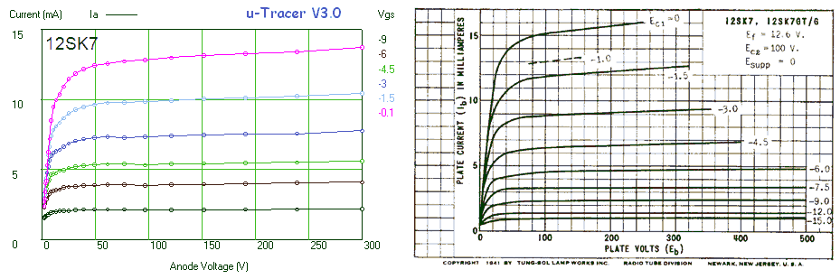
Figure 16.19 12SK7 Remote cut-off IF Amplifier
After surfing the web a bit more, I found that my Pilot radio is - what the Americans call - “an all American five.” What this means is that it is a kind of a minimal radio with five tubes, in which everything has been done to reduce the costs. One characteristic of this type of radios is that they don’t use a mains transformer, but that the high voltage was directly taken from the mains. Additionally, the filaments of the tubes were designed in such a way that they all operate at the same current so that all the filaments could be placed in series. Tube manufactures designed special series of tubes, called line-ups, which together made a radio, and which were designed in such a way that the total filament voltage of all the filaments in series was equal to the mains voltage. The tubes were often multi-purpose tubes which e.g. combined functions of amplification and detection, or oscillation and frequency conversion.
Notwithstanding the term “all American Five,” these sets where produced by almost any radio manufacturer, all around the world. Despite the fact that these radios were very cheap and popular, they had one huge disadvantage: the chassis was directly connected to the mains so that every contact with any metal part of the radio could be lethal!
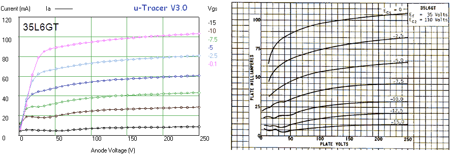
Figure 16.20 35L6GT Beam AF Pentode. An external power supply was used for the filament.
My Pilot T-502 contained the following tubes: a 12SA7 RF mixer/oscillator, 12SK7 Remote cut-off IF Amplifier, 12SQ7 Double-diode triode/2nd IF amplifier and detector, 35L6GT Beam AF Pentode, and finally a 35Z5GT high voltage rectifier. The 35L6GT didn’t correspond to the circuit diagram which specifies a 50L6GT. Both tubes are in fact identical, the only difference being that the first one has a filament voltage of 35 V, while the second tube has a filament voltage of 50 V. I guess that at a certain moment somebody (it must have been my father) replaced a defect 50L6GT for a 35L6GT. The lower filament voltage was compensated for by a big power resistor in series with the filaments inside the chassis. Although the 35L6GT was still perfect I will try to get my hands on an original 50L6GT to restore the radio to its original state.
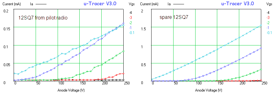
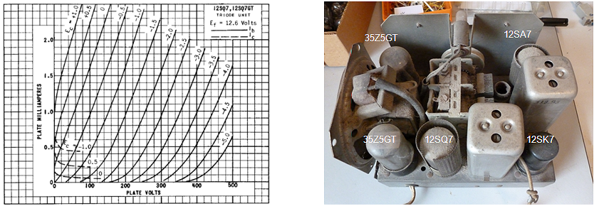
Figure 16.21 12SQ7 Double-diode triode, 2nd IF amplifier and detector
After some testing the culprit was quickly found: a nearly dead 12SQ7 IF amplifier/detector. For a moment I thought I was lucky because I found another 12SQ7 in my collection, but that one also had a very poor emission. In other words, the search has started for a “new” 12SQ7 to get my set playing again.
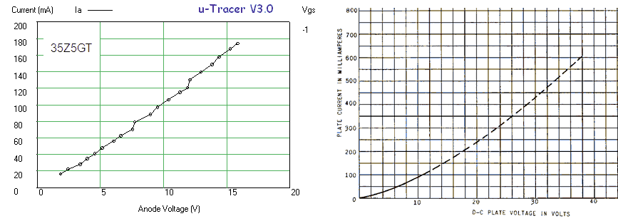
Figure 16.22 35Z5GT high voltage rectifiers. An external power supply was used for the filament.
Decent testing of the 12SA7 hexode (“pentagrid”) frequency changer tube was a bit less straightforward. Philips e.g. publishes DC curves of their hexodes, but these were not available for the 12SA7. However, probably for testing purposes, the datasheet states some DC characteristics of the tube in “non oscillating” mode. With the anode and screens connected to 100 V, and the grids to 0 V, the cathode current should be around 25 mA (I assumed that the suppressor grid was kept floating). Figure 16.23 shows a set of Ia(Va) curves of the 12SA7 tested in this configuration whereby the anode voltage was varied between 0 and 100 V, and the first control grid voltage was stepped from -7 to 0 V. The very last point measured corresponds to the point mentioned in the datasheet, and the anode very nicely matches the current specified in the datasheet (25 mA).
Figure 16.23 12SA7 RF mixer/oscillator.
The PCL85 and PCL805
The PCL85 / PCL805 is a triode / pentode combination used as frame oscillator and output stage in black and white televisions sets with 110 degree deflection. The control and screen grids have been aligned to reduce the screen current. The tube does not have an audio output rating, probably because of the rather large “tetrode kink” which is still present in the output characteristics despite the pentode configuration. That is also the reason why the tube fascinated me. The “tetrode kink” has my fascination because it is such an interesting physical phenomenon. According to the datasheet the kink could be so large the near cut-off the anode current could become almost negative!
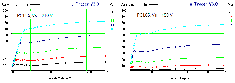
Figure 16.24 Output curves of the PCL85 at Vs = 210 and 170 V
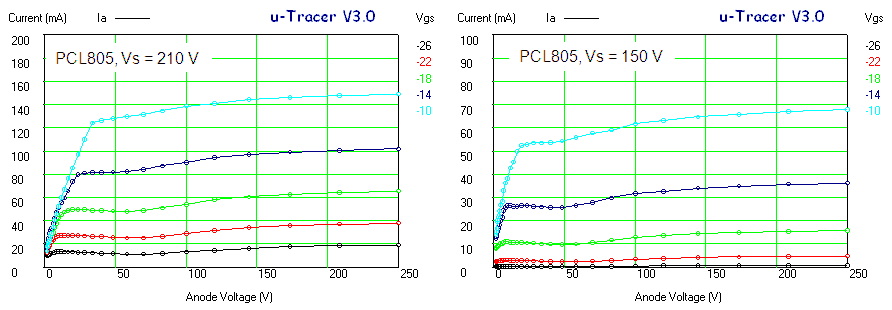
Figure 16.25 Output curves of the PCL805 at Vs = 210 and 170 V
I tested both the PCL85 as well as the PCL805 which is supposed to be an improved version of the PCL85. The kink turned out to be not nearly as “good” as I had hoped for. Both the tubes have a very pronounced kink which is smaller than the kink in the datasheets. The difference between the characteristics is only very small.
The ECC86, ECH83, EF97, EF98, EBF83 low-voltage car radio tube series.
Before the advent of transistors, car radios were made using radio tubes. For the generation of the high voltage a mechanical vibrator (“triller”) in combination with a transformer was used. Apart from the fact that such a circuit was rather bulky and unreliable, it also made a lot of noise, both audible and RF! No wonder that manufacturers (and custumers) jumped at the possibility of replacing tubes with transistors as soon as they became available. Unfortunately the first transistors were only suitable for application in the low frequency audio part of the receiver. In the transition phase from tube radios to fully transistorized receivers in the late fifties, Philips introduced hybrid receivers in which the RF circuits used tubes, while the AF circuits employed transistors. Special tubes were designed which could operate at anode voltages as low as 12 and even 6 V. Although these tubes were suitable for high frequency operation, they couldn’t deliver any power. That was not an issue because the transistors took care of that. In this way a completely low-voltage receiver was realized.
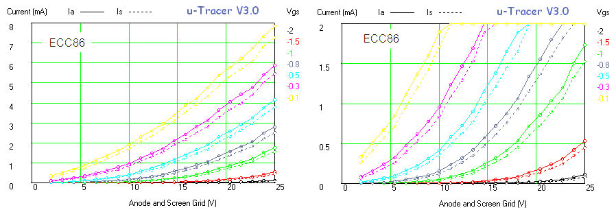
Figure 16.26 Ia(Va) curves of the ECC86
The low-voltage car radio line-up consisted of a complete series of tubes: the ECH83 triode-heptode frequency changer, the EF98 and EF97 IF amplifiers (EF97 var. mu), the EBF83 IF amplifier plus detection and AGC diodes and finally the ECC86. The ECC86 was used as a grounded grid VHF amplifier and self-oscillating mixer. The fabrication of these very low voltage tubes had become possible by using very tight fabrication tolerances and modern frame-grids (“spanroosters”). It appeared that the fabrication tolerances where so critical that there was quite some tube-to-tube variation. Consequently the radio had to be re-aligned after a tube change. An example of a radio which used these tubes was the
Paladin ND484VT (more info Here.)
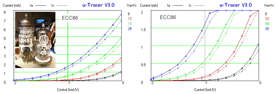
Figure 16.27 Ia(Vg) curves of the ECC86 low-voltage tube.
Figures 16.24 and 16.25 shows the output- and Ia(Vg) curves of an ECC86. The maximum allowable anode voltage if 30 V! Despite the very low anode voltage, the mutual conductance, according to the datasheet, still amounts to 2.6 mA/V.
The EL34, Output Pentode.
The EL34 is a 25 Watt audio output pentode. It was introduced around 1950 as the EL60 by Philips / Mullard in an “all-glass” envelop and a 9 pin Loktal (like the EF50) base. The Loktal base was not very popular so a few years later the EF60 was re-introduced as the EL34. The EL34 was and still is high popular. It was especially popular in (British) guitar emplifiers. It is one of the few years that is still in production more than 60 years after its first introduction, but not by Philips. The El34 has become a bit of a cult object amongst audiophiles, especially the original Philips / Mullard tubes. Some web shops ask crazy prices of up to $550 per tube! There are a number of excellent articles on the web on the EL34 and its history (Link 1, Link 2, Link3).
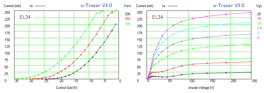
Figure 16.28 Ia(Vg) and Ia(Va) curves of a real nickel base Philips EL34 (Vs = 250 V).
I am lucky to own several EL34s but I never payed $550 for any of them! The tubes are specified for anode voltages up to 800 V. I tested them up to 250 V with compliance protection switched off! In this way it is possible to measure anode currents up to 250 mA when the hardware current limit kick in (observe the leveling of the anode current in Fig. 16.28 left for currents around 250 mA).
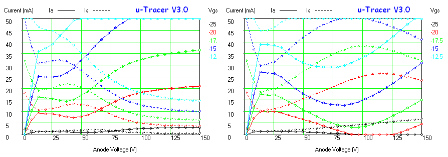
Figure 16.29 Close-up of the output curve for “low” anode voltages of an EL34 in pentode (left) and tetrode (right) configuration.
Interested in “tetrode kincks” I measured the EL34 also in tetrode configuration, so with the suppressor grid tied to the anode instead of to the cathode. Figure 16.29 shows a close-up of the output curves for “low” anode voltages in pentode (left) and tetrode (right) configuration. The drawn lines represent the anode current while the dashed lines represent the screen current. Near cut-off the secondary emission in tetrode configuration is so high that the anode current becomes negative! The anode is now literally acting as an emitter!
The EC50, Thyratron.
The EC50 is a helium filled thyratron introduced around 1939. A thyratron is a high voltage power switch very comparable to a thyristor. When the anode current is raised with the grid at a negative potential there is no anode current. However, is the grid is shortly made positive a plasma ignites and a current starts to flow limited by an external resistor. The current continues to flow even if the grid is made negative again. The plasma only extinguishes when the anode voltage is reduced to zero again.
When the tube is ignited there is a voltage drop of about 33 V between anode and cathode.
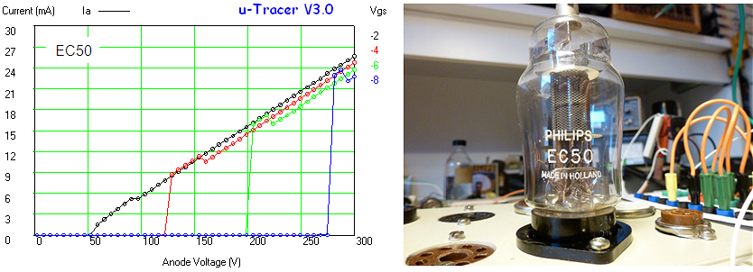
Figure 16.30 Ia(Va) curve of the EC50 for different Vg with an anode series resistor of 10k.
The tube can however also ignite when the anode voltage is increased beyond a certain critical value. This value depends on the negative grid bias. The more negative the grid, the higher the ignition voltage. The relation between the negative grid bias and the ignition voltage is almost linear. In Fig. 16.30 an Ia(Va) curve is measured of an EC50 for different grid bias values. To limit the current a 10k resistor was switched in series with the anode lead as represented by the slope of the straight line.
KT120, an enormous modern audio pentode
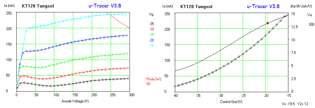
Figure 16.31 Ia(Va) and Ia(Vg) curves for a Tung-Sol KT120. The screen voltage in both cases was 300V.
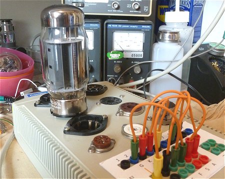 Personally I have little affinity with tube amplifiers and consequently my collection of tubes encompasses only the old well known audio tubes such as the EL84 and the EL34. A visit from a potential uTracer customer however, gave me the opportunity to test a modern state-of-the-art KT120 power audio pentode. The KT120 is claimed to by the most powerful audio tube in production, and in push-pull it can deliver 150W of audio power.
It is really a monster with a maximum anode dissipation of 60W and a filament current of 1.9A at 6.3V. My visitor wanted to see if the uTracer was capable of tracing this tube. The first measurement with a grid voltage of -10V immediately drove the anode supply into compliance. However, after some searching for the optimum bias conditions, we were able to trace a nice set of curves pushing the uTracer to the limits of its capabilities by driving the tube at an anode voltage of 300 V at a current of 250 mA, just into the “forbidden” dissipation regime of the tube (Fig. 16.31 left).
I was a bit afraid that the 1.9A / 6.3V heater would be a bit too much for the internal heater supply of the uTracer, but actually it pulled it off quite well. From the Ia(Vg) we extracted a transconductance of 13 mA/V at Va=Vs=300 V, Vg=-20V at an anode current of about 220 mA. Luckily the plots convinced my customer and he left being the proud owner of a kit. I hope to see some more KT120 plots of him in the future!
Balanced valves? Might be – might not! By: Robin Simmons
Example of valves appearing to be fairly closely matched when comparing characteristics at the manufacturers’ nominal bias/current operating point compared with what happens when measuring at the amplifiers design operating point.
Traces below were obtained when measuring the characteristic of 4 valves in an old ‘Fender Twin Reverb’ guitar amp using 6L6GC valves stamped as ‘International C Servicemaster‘ (USSR). First impression is that the valves have a similar characteristic and should be OK for further use in a push-pull amp configuration.
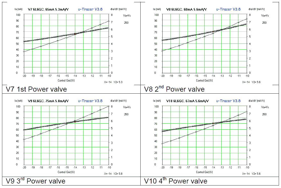
After carrying out some repairs, the amp was turned on and after warming up, the anode current was checked for each valve at the amps normal bias operating point of approximately -52V. Anode voltage is 440V. The following results were obtained.
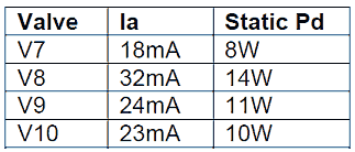
Obviously the anode currents are significantly different than might be anticipated from the previous test results. The valves were then re-tested under the nearest conditions to the amps operating point as could be obtained with the uTracer. The results are shown below.
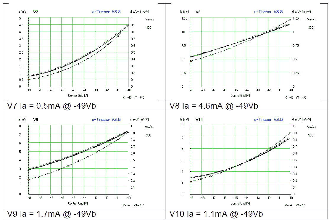
This shows how misleading it can be to test valves against data sheet performance compared with how they may actually be used in real world applications. It is also ‘ammunition’ in the argument for uTracer to have a wider range of grid bias capability plus higher anode voltages as has already been discussed on the blog. This would enable testing of valves such as EL34’s and 6L6’s under conditions much closer to how they are actually used in audio amps and hence reveal problems that may not
otherwise be so obvious.
Summary
So far the uTracer V3 hasn’t disappointed me at all, on the contrary it is really a pleasure to work with. As mentioned at the beginning of this section, especially the auto-range and auto-average options make it a truly pleasant and professional tool to work with. This of course doesn’t mean that there is nothing to improve. Here is a list:
| to top of page | back to homepage | to part I |
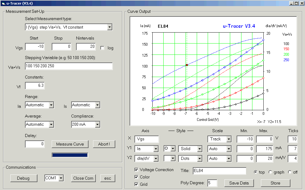
Figure 17.1 Layout of the Version 3.4 Graphical User Interface
It has cost me a number of weeks of programming, and therfore it is not without pride that I can now present the completely renewed Graphical User Interface (GUI) for the version 3.4 uTracer. With respect to the GUI for the uTracer 2 many new features have been added:
| |
|
|
|
|
|
|
|
Click on one of the images for a guided tour through the new GUI!
Figure 17.1 shows the main “form” (a Visual Basic term) of the GUI. There are three areas on the form. The upper-left area is for the measurement set-up. Things like the type of measurement, the voltage ranges and details about range selection, averaging and current compliance can be set here. The whole right part of the form is for the graphical output of the measurement data. The small section at the bottom-left deals with the communication between the GUI and the uTracer.
Measurement Setup
The set-up of a new measurement is very simple and intuitive. The best thing is to go through the measurement set-up section from top to bottom. Most settings have been pre-programmed or are automatic so that usually very little adjustments are necessary. The most important thing to specify is the type of measurement. This is done by selecting one of the measurement types from the drop-down menu on the top of the form (Fig. 17.2). At the moment in total 6 measurement types have been defined. The most important ones are the anode (and screen) current as a function of grid bias “I(Vgs) step Va, Vs, Vf constant” and the currents as a function of the anode voltage “I(Va) step Vgs, Vs, Vf constant.”
The next thing to set are the measurement voltages. Selection of a new measurement type will automatically copy a set of default values into the voltage selection text boxes. In most cases these default values will already produce a nice set of curves, but of course the values may be changed as required. The following minimum and maximum values need to be observed: the anode and screen voltages have to be within 2 to 300 V, the grid bias between -50 and 0V, while the filament voltage must be between 0 and the power supply voltage (19.5 V).
In most cases this is enough to set-up the GUI and can a measurement be started. This is done by pressing the “Heater On!” button. The heater will now be slowly switched on with increments of 10% of the nominal heater voltage a second. When the filament is already hot, or when you don’t care about a slow-startup of the heater, the button (which now displays “Heating …”) can be pressed again which will apply the full nominal heater voltage to the filament. It is up to the user of the GUI to decide when the tube has stabilized enough to start a measurement. Pressing the same button again (which now displays the text “Do Measurement”) will start the measurement. Both the measurement as well as the heating of the filament can be interrupted at any time by pressing the “abort” button. Since the scales of the axis in the output section are set by default to “Automatic Scaling,” the measurement will always result in a nice picture.
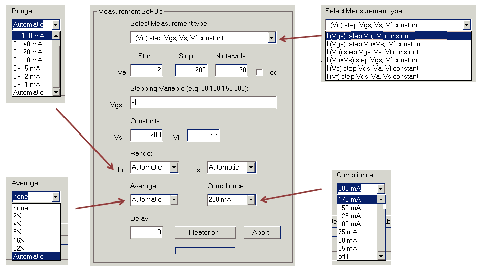
Figure 17.2 Measurement Setup section of the GUI.
In the drop-down boxes captioned “Range:”, the measurement range can be selected. Normally, it is best just to leave the ranges set to “Automatic.” There are however two situations in which you might want to set the range manually. The first situation occurs when you want to make a very nice and smooth graph of a set of curves, and there is a change of measurement range in the middle of a curve. Sometimes this can result in a small “bump” or “dip” as a result of small gain differences, although the effect is usually very small (the PGA113’s are really very good). In that case a fixed gain can give a better result. The other situation occurs when the screen current is not measured:
Tip! When the screen current is not measured[R1], e.g. in the case of a diode or a triode, the uTracer will increase the gain of the screen current channel to maximum. This in turn will cause the averaging algorithm to increase the number of averages. For the anode
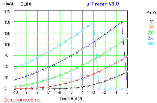 current this may not be necessary, but since the anode and screen currents are measured simultaneously, the additional averages will slow down the whole measurement process unnecessarily. Ii is in that case best to set the screen current range fixed to 200 mA.
If you are in a hurry, and don’t care too much about a bit of noise in the Graph, but just want to get a quick impression of the quality of a tube the averaging can be switched of by selecting the proper option in the “Average:” drop down box. Alternatively a higher number of averaging can be specified to get an even better quality graph.
Finally there is the menu where the user can select the current compliance. I think I already mentioned a few times on this page that there are two “over-current” protection mechanisms in the utracer 3. In the first place there is a very fast hardware protection which simply limits the maximum current to 250 mA. Then there is a second, programmable protection mechanism – the current compliance - which, since it is software controlled, is a bit slower (typically 10-20 us). This second mechanism protects the high voltage switch against excessive dissipation during a short-circuit. The user can set the current compliance to a number of values between 0 and 200 mA. The compliance applies to the anode current as well as the screen current. It is also possible to switch the compliance protection off! I would not recommend using this setting unless you are absolutely sure that the tube is ok, because a flash-over in that case will surely destroy the high-voltage output transistor. The measurement range is extended to 250 mA when the compliance is switched off.
Finally there is a last box where a delay can be specified which is inserted after every measurement. This delay can be very useful when e.g. a magic-eye is tested.
Graphical Output Section
Not only the appearance of the graphical output section has been thoroughly revised, also the structure of the program behind it has been completely renewed and especially restructured. Many new features have been included such as a second independent Y-axis, extraction / plotting of the transconductance and output resistance, and the implementation of a smart cursor.
Figure 17.3 Graphical output section of the GUI.
Just beneath the plot are the controls which determine what is plotted and how it is plotted. The controls have been organized into three rows. The top row for the X-Axis, the second row for the first (left) Y1-axis and the bottom row for the second (right) Y2-axis. The X-axis variable is always identical to the “running” variable specified in the Measurement Setup section. For both Y-axes the user has the possibility to choose from 7 variables (Fig. 17.3). The first two are the anode and the screen currents. The next three parameters are related to the plotting of the transconductance and I will come back to those later in this section. Finally the last two variables retrieve the stored data. Just like in the version 2 GUI, the anode and screen currents can be stored for comparison with a new measurement by pressing the “Store” command button. This feature can be used to compare or match tubes.
There are a number of options to scale the axis, and the options differ slightly for the different axis. By default the scaling of the X-axis is set to “Track.” This means that the minimum and maximum values along the X-axis are copied from the start and stop values from the “running” variable in the measurement setup section. A small thing needs explaining here. Because of the way how the uTracer is constructed, the minimum anode and screen voltages cannot be lower than 2 V. Having 2 V as a lower X-axis value looks a bit silly, that is why the software, when it detects that a minimum X-axis value lower than 2 V has been entered, automatically sets it to 0 V. Alternatively the user can set the minimum and maximum values of the X-axis manually.
Both the Y-axes are by default set to “Automatic.” A special algorithm ensures that there are always “sensible and round” numbers along the axes and that the number of marker ticks is adjusted accordingly. Next to the possibility to set the axes manually, there is also a “Track” option. When this option is selected, the maximum axes values are copied from the selected range in the measurement setup section. The second Y-axis has a fourth option “Copy”. In this case the minimum and maximum Y2-Axis values are always copied from the Y1-Axis, even if the scaling for that axis is set to “Automatic”.
All the other plot settings and options are pretty straightforward; the only item left to discus is a check box captioned “Voltage Correction”. As a result of the voltage drop over the current sense resistor and the discharging of the buffer capacitors, the actual anode and screen voltages on the tube will be somewhat lower than the voltage to which the anode and screen buffer capacitors have been charged. Fortunately these (most of the times very small) voltage drops are known and can be corrected for. This is why sometimes in e.g. an output characteristic the plotted anode voltage at high current levels can be a bit lower than the set anode voltage. With the check box in this section the user has the possibility to switch the anode voltage correction off.
Measuring the transconductance and output resistance
The transconductance of a tube is the variation in anode current as a result of a small variation in gate voltage at a certain bias point, which is nothing more than a combination of DC grid and anode voltages. In other words, it is the slope of the anode current versus grid voltage at a specified bias point. In mathematical terms: the transconductance is the first derivative of the anode current with respect to the grid voltage.
This simplest way to measure the transconductance is to draw a line through two consecutive data points on the Ia(Vgs) curve. The transconductance is then nothing else than slope of this line. However, differentiating a measured curve this way usually results in a very noise transconductance curve as a result of (small) fluctuations in the measured data. In the version 3 uTracer I have therefore used a slightly different approach. After measurement of a set of Ia(Vgs) curves, first a polynomial is fit through the measurement points. This polynomial smoothes out the fluctuations in the measured data. After the fit the polynomial is analytically differentiated resulting in a perfect noise free transconductance curve.
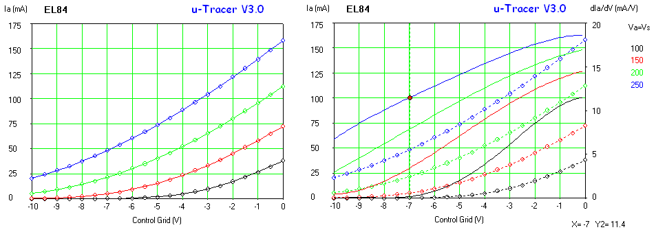
Figure 17.4 Left: Ia versus Vg set of curves for an EL84; Right: extracted transconductance (solid lines) and anode current (dashed lines)
Figure 17.4 shows an example of a transconductance “extraction” from a set of Ia(Vgs) curves. The original set of curves is shown on the left. The first step to extract the transconductance is to determine the degree of the polynomial to be fitted. The degree of the polynomial can be set to any value between 1 and 25! I usually do this by trial and error. I usually plot the data on the Y1-axis and then switch off the line so that only the markers are shown. On the Y2-axis the fitted anode
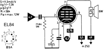 current is plotted with the markers switched off. In this way it is easy to compare the fit to the measured data. A 5th order polynomial usually gives a good result. The order of the polynomial should not be chosen too high because that will result in oscillations in the transconductance curve. When the fit is ok, the derivative of the current to the voltage (dIa/dV) can be plotted. An alternative way to find the optimum polynomial degree is to directly plot the transconductance, and
then to vary the polynomial degree. At first increasing the order of the polynomial should result in a significant change in the transconductance curves. At a certain point the curves will not change anymore when the order is increased. However, when the order is increased again beyond a certain point oscillations in the transconductance curves will appear. The most optimal point is somewhere in the flat part where the transconductance is relatively independent of the degree of the polynomial. The right graph in Fig. 17.4 shows the extracted transconductance (solid lines) and the original anode current as a function of grid bias. The marker shows the transconductance at the bias point recommended in my “Muiderkring” tube handbook (see inset) Vg = -7 V and Va = Vs = 250 V. Both the transconductance as well as the anode current are exactly the same as the values mentioned in the handbook, respectively 11.5 mA/V and 48 mA, which shows what an accurate and useful instrument the uTracer is!
current is plotted with the markers switched off. In this way it is easy to compare the fit to the measured data. A 5th order polynomial usually gives a good result. The order of the polynomial should not be chosen too high because that will result in oscillations in the transconductance curve. When the fit is ok, the derivative of the current to the voltage (dIa/dV) can be plotted. An alternative way to find the optimum polynomial degree is to directly plot the transconductance, and
then to vary the polynomial degree. At first increasing the order of the polynomial should result in a significant change in the transconductance curves. At a certain point the curves will not change anymore when the order is increased. However, when the order is increased again beyond a certain point oscillations in the transconductance curves will appear. The most optimal point is somewhere in the flat part where the transconductance is relatively independent of the degree of the polynomial. The right graph in Fig. 17.4 shows the extracted transconductance (solid lines) and the original anode current as a function of grid bias. The marker shows the transconductance at the bias point recommended in my “Muiderkring” tube handbook (see inset) Vg = -7 V and Va = Vs = 250 V. Both the transconductance as well as the anode current are exactly the same as the values mentioned in the handbook, respectively 11.5 mA/V and 48 mA, which shows what an accurate and useful instrument the uTracer is!
Exactly the same procedure is followed to extract the output conductance of a tube. In that case the anode current is measured as a function of anode voltage. Since it is more common to give the output resistance it is also possible to plot the reciprocal of the conductance: dV/dIa.
The Communications Form
The last part left to explain is the communications section on the lower left part of the form. With a drop down menu it is possible to use another COM port than the default port 1 if needed. Furthermore there is a button to close the current COM port or to send an escape character to the utracer. An escape character always forces the uTracer to return to its reset state.
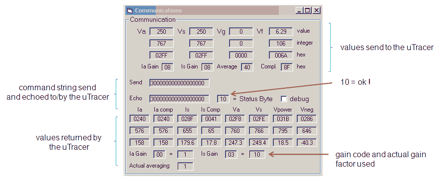
Figure 17.5 Communication debug form.
Pressing the “Debug” command button opens a second form with detailed information about the communication between the GUI and the uTracer. This window was used extensively during the debugging phase of the program development, and I still use it regularly to check what is going on in detail. Detailed information on the communication protocol can be found in Section 15 of this page. The form has three areas, the top part displays data that is send to the uTracer by the GUI. In the four columns we find the set-points of the voltages which together determine the bias point of the tube. The top row gives the decimal value. The row below that gives an integer representation of the set-point which has been translated to a value which makes sense for the 10-bit on-chip AD/PWM converters. The row below that just gives the hex representation of the integer value. The last row gives the values for the gain, averaging and compliance settings which are send to the uTracer in the command string. These last values are already coded so that the uTracer can easily interpret them.
The four setpoints, headed by a command byte are combined to a command string which is shown in the middle section of the form. Normally the uTracer echoes every character sent to it. This process is monitored in the line below the command string which shows the echoed characters.
In the bottom section of the form the data is displayed which is sent back by the utracer in the result string. The result string is composed of three parts (see Section 15). It is headed by a status word which is displayed separately. A value of 10 indicates a successful measurement, while 11 indicates the occurrence of a compliance error. The bulk of the data in the result string is the readout of the 8 AD channels. The hex readout and the integer representations are shown in the top two lines. In the row beneath that the decimal value is shown whereby already the conversion from AD readout to real voltages and currents has been done. In the boxes at the bottom the actual gain and averaging values which were used for that particular measurement point are shown. They may vary from point to point when the automatic ranging and averaging options have been chosen. It is instructive to see them change during a measurement.
Things left to do
It is only after writing of a section like this that one comes up with a list of things which are still missing or which still have to be done. Here are a few of them:
| to top of page | back to homepage | to part I |

Since the writing of the previous sections the wish list at the end of that section has been implemented. There are now already so much changes that just for the sake of documentation the version number of the GUI has been increased to V3.5. With respect to the previous version, V3.5 includes: storing of measurements in two different formats, storing of the graph in a bmp file, a new form with sliders that can be used to calibrate voltages and currents, saving of the calibration data in a calibration file which is automatically loaded at start-up, plotting of a load line, plotting of a maximum dissipation hyperbole, implementation of a “ping” function which returns the analog values of the eight AD input channels, automatic measuring of the uTracer supply voltage which is an important system constant in the GUI.
The general structure of the GUI is basically the same as the structure of the version 2 GUI. in this section, again mainly for the sake of my own documentation a number of specific topics related to the version 3 GUI will be discussed.
The way data is stored internally.
Just as in the version 2 GUI all the measurement data is stored in a large array. In this array each row is an individual measurement, while the columns represent the current and voltage values. For the version 2 GUI the array had only 200 rows, limiting the number of measurements to 200. There was a separate array which held the stored data.
In the version 3 GUI things have changed in the sense that all the data is now stored in one large data array “dblMeasMX(3000,6)”, which is subdivided into three different areas (Fig. 18.1). Rows 0 to 999 hold the actual measurement data so that the total number of measurements is extended to 1000. When the “Store” command button is pushed, the actual data is copied to region consisting of rows 1000 to 1999. The region 2000 to 2999 holds the simulated data. This is the area where the fitted data is stored for representation. The different columns hold the different voltages and currents. The definition of the columns varies slightly for the different areas (Fig. 18.1). The advantage of storing all the data in one array is that in this way all data to be plotted (the curves) can be addressed by a row number and the column numbers for the x- and y-axes.
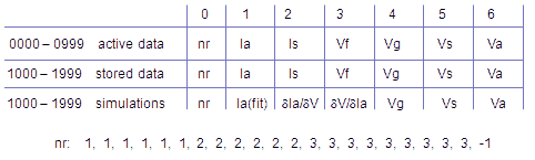
Figure 18.1 Structure of the Measurement Matrix.
When a set of curves is addressed by a row number, the row number always points to the first data point of the first curve. Column 0 holds the curve number which is 1 for the first curve. Each next row with the same curve number belongs to the same curve within a set of curves. When the curve number of a next row is incremented with respect to the previous row, it indicates the start of a new curve. The end of a set of curves is indicated by a curve number -1. This row is not part of the curves. The number of datapoints within a curve us thus nowhere specified explicitly. Also the number of datapoints for each curve within a set of curves may vary. Figure 18.1 gives an example of a sequence of curve numbers. In this example there are three curves: curves one and two consisting of six data points while the third curve consists of eight data points.
”Do Ping”
The supply voltage is an important system parameter for the GUI. First of all because the filament voltage is directly related to it. Additionally the anode and screen voltages are set with respect to the supply voltage. I use an old 19.5 Dell laptop power supply, but I wanted to keep the uTracer flexible in the sense that also other laptop power supplies with voltages in the range of 17 – 22 V could be used. For this reason the supply voltage is directly measurable through one of the AD input channels. In fact it is automatically measured during every measurement and available on the “Debug Form.” However, to be able to set this important system variable during start up it was necessary to measure the supply voltage without doing a complete measurement cycle. For this purpose the “ping” command was defined.
The ping command does nothing more than to send a command to the uTracer to read out the eight AD channels and to send back a result string with the values. As said the command is used during the initialization of the GUI, but for debugging purposes the user can also issue a ping command by pressing the ping command button on the debug form. Actually not one command, but two commands are send to the uTracer. The first command is the “00” settings command which ensures that the PGAs are properly set. The second command is the newly defined “50” ping command. The returned values are temporarily stored in measurement matrix location 999. When the returned power supply value is out of the 17 – 22 V range a default value of 19 V is used.
GUI State Diagram
The version 2 GUI knew 3 internal states: 0= all off, 1 = filament on, 2 = measurement in progress. With the introduction of the “soft filament startup” it became necessary to revise this scheme and to introduce more states. Figure 18.2 shows the revised state diagram of the version 3 GUI.
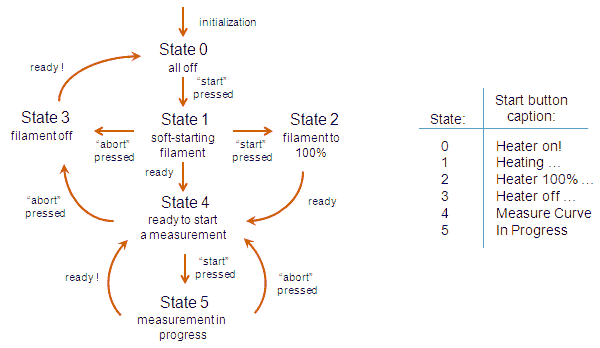
Figure 18.2 State diagram of the version 3 GUI.
On initialization, the GUI is set to state 0 meaning that filament is off and no measurements. Pressing the start command button moves the GUI to state 1 and will cause the execution of “a ping” to measure the supply voltage and will execute routine “DoHeater.” This routine increases the filament bias from 0 to 100% of the set point value in 10% increments every second. When the set point is reached, the “DoHeater” routine will move the uTracer to state 4. Pressing the start button during this state will immediately move the GUI to state 2 so that the filament is directly heated to its final point value. Pressing the stop button during this state will switch the filament off (via state 3) and return the GUI to the ground state. In state 4 the GUI is waiting for the user to press the start button again to start the actual measurement. This will cause the GUI to move to state 5 and execution of the “DoMeasurement” routine. After every change in state routine “CommandUpdate” is called which modifies the caption of the start button depending on the state the GUI is in (Fig. 18.2).
Calibration
Something which was for a long time on the “wish-list” of things to be added to the GUI was the possibility to calibrate the different voltages and currents. So far the value of the applied voltages and the measured currents completely depended on the accuracy of the resistors used and the 5V supply voltage of the microcontroller which is used as the voltage reference for the AD conversion.
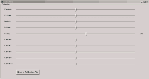
Figure 18.3 The calibration form (not yet completely finished).
In the version 3.5 GUI the possibility to calibrate the different voltages and currents has been implemented by means of an additional form (Fig. 18.3). The form contains a number of sliders which can be set to a value between 0.9 and 1.1. Each slider is used to correct a voltage or a current. The top slider e.g. “Va Gain” can be used to compensate for the tolerances in the high voltage divider and the 5 V supply reference. Basically what is done is that in most cases the variables are just multiplied by the calibration value. At a later stage the correct calibration procedure will be discussed. The position (value) of the sliders are linked to ten public variables dblCalVal1 to dblCalVar10. After a slider has been moved, its new position will immediately effect the next measurement.
Pressing the “Save to Calibration File” button, will save the slider positions to a file named “uTracer_3p4.cal.” This is a simple readable/editable ascii file consisting of ten lines, each line starting with the corresponding calibration value, followed by an explanatory text string which is further ignored. Upon startup of the GUI (loading of the main form) routine “LoadCalFile” is executed. This routine first checks if the calibration file is present. If so, it is loaded. If not a new cal file is generated in which all the calibration values have been set to 1.0.
Structure of the plotting section
Mainly because of the introduction of the possibility to extract the transconductance and the option of two independent y-axes, the plotting part of the GUI version 3 had to be completely revised. It has now a more logical and modular structure. The main routine which is called by the program when the graph has to be refreshed is “DrawPicture”. This routine calls a large number of other routines which together build up the graph. Before the routine erases the existing graph, it prepares a number of things so that the buildup of the new graph takes as little as time as possible. These activities include: selection of variable to be plot, curve fitting of data if required, positioning the cursor if required, and performing the auto-scale function.
 The x-axis variable is always equal the “running” variable defined in the measurement section, and it is the public variable intColumnVar1 which holds the column number of the x-axis variable in the measurement matrix. The y1- and y2-axes variables are selected by the user in the “combo boxes” in the plotting section. The first thing which happens after a call to “DrawPicture” is that, depending on the selection by the user, the variables intY1row, intY1col, intY2row, and intY2col are pointed to the location in the measurement matrix where the data can be found.
The next thing is the fitting of the polynomial(s) to the measured data if needed. The whole process of fitting the data and generating the fitted curves as well as the transconductance is done by routine “CurveFit.” This routine is called only if: 1. The user has requested the plotting of one of the fitted / extracted variables (Ia_fit, dV/dI, dI/dV), AND, 2. There is at least one measured curve (MeasMx(0,0) <> -1), AND, 3. The uTracer is not actively measuring a set of curves ( State <> 5). In a separate section the structure of “CurveFit” will be discussed in more detail.
The following actions concern the scaling of the x- and y-axes. If the option automatic has been selected for the x-axes, the start and stop values for the running variable Var1 are copied from the measurement set-up section. There is one small complication here. Because it is not allowed to use a start value for the anode and screen voltages lower than 2 V, using this minimum value would result in a rather strange x-axis annotation. For this reason the routine will set the minimum x-axis value to zero when it is smaller than 2.1 V. When automatic scaling of the y-axes is selected, the minimum value is set to zero while the maximum value is determined by routine “FindMax.” This routine not only finds the maximum in a set of curves, but also has an algorithm to chose a pleasant and sensible maximum axis value with corresponding number of y-axis marker ticks.
After all these preparations the current graph is erased and a new graph is plotted. The structure of this section is rather straight forward with routines to draw the grid, legend, logo, axes etc. The curves are drawn by routine “drawcurve” which uses as input the row number of the starting point of the set of curves and the column numbers for the x- and y- values. Finally, when the user has clicked with the mouse on the actual graph area (blnMouse = true), routine “ReadCurve” is executed. This routine places the cursor on the nearest point of the nearest curve and displays the y-axis value.
Polynomal fitting and extraction of the transconductance
The first step in the extraction of the transconductance (in case of a Ia(Vg) measurement) or the output resistance (in case of a Ia(Va) measurement) is the fitting of a polynomial through the measurement points. For this I used a very useful piece of code written by Frank Schindler in 2000! He provided a class (RegressionObject.cls) as an easy way to implement polynomial regression to any visual basic application. I do not remember where I found it on internet, but I include the original zip file containing the class code, an example and some explanatory text here. The help document in the zip file clearly explains how the class works. After the data points of the curve are entered, the coefficients of the polynomial can be retrieved. The order of the polynomial can have any value between 1 and 25! The regression class works very reliable and stable.
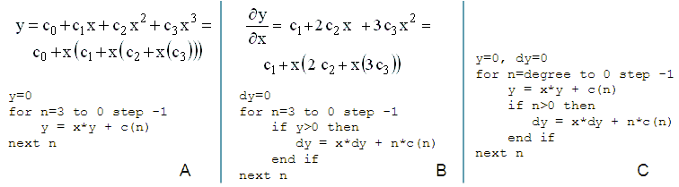
Figure 18.4 Evaluation of the polynomial and its derivative from the coefficients.
The curve fitting and extraction of the derivatives is done in routine “CurveFit”. Inputs to the routine are the row number where the curve starts, the column number where the x-axis variable can be found (the y-axis variable is always the anode current Ia), the degree of the polynomial, and the minimum and maximum x values required for the generation of the simulated curves (the Xmin and Xmax values of the plot). The routine deals with each curve in a set of curves individually. First it initializes the regression object. Next the data points in the curve are entered into the object. After entering the points the coefficients of the polynomial are available. Finally, using these coefficients the routine generates a curve of the fitted anode current and its derivative over the x-interval specified consisting of 100 data points. The generated curves are stored in the “simulations” area in the measurement matrix. Not only the derivative, but also the reciprocal of the derivative is stored. After all curves in a set of curves have been processed, the data is terminated with a -1 curve number. In this way the simulated curves can be dealt with by the plotting routines in just the same way as ordinary measurement data.
For the evaluation of the polynomial(s) I have avoided the use of the time consuming exponentiation function x^n. Using a third degree polynomial as an example, Fig. 18.4A shows how the ordinary polynomial form can be rewritten as a product of first order terms, and how a simple loop can be used to evaluate the expression. The derivative of the polynomial can be evaluated in a similar way (Fig. 18.4B). To reduce the evaluation time as much as possible the evaluation of the polynomial and its derivative have been merged as sown in Fig. 18.4C.
Implementation of a cursor.
Although it started as a kind of “nice to have gadget,” the cursor function actually turned out to be quite useful. The “deluxe” cursor features a snap-to-curve action, and even extrapolates between measurement points. When a “mouse-down” event is detected in the picture field, the event routine retrieves the mouse coordinates and when they are within the actual graph area sets flag “blnMouse.” It then calls routine “DrawPicture” to refresh the graph. At the end of “DrawPicture,” the routine checks if “blnMouse” is set, end if so calls “ReadCurve” to add the cursor to the plot
Figure 18.5 Algorithm used to scan the curves for two consecutive points.
Input to “ReadCurve” is the x-value of the mouse click. The routine scans each curve in a set of curves to find two consecutive points of which the first point has an x-value that is smaller than the x-coordinate of the mouse, while the other point has a larger x-coordinate. Figure 18.5 shows a part of this algorithm, it singles out two points i, i+1 which are always on the same curve while all points on the curve are considered. When the two points encompasing the mouse position are found, the routine determines a straight line through these points:

On this line the exact y-value corresponding to the x-value is found. This y-value is now translated back to the integer picture y-coordinate. From the picture y-coordinate and the y-coordinate of the mouse the vertical distance between the mouse and the curve is determined. Going through the curves the minimum distance and corresponding curve are recorded. Finally the x- and y-values are plotted at the bottom of the graph.
X-axis ticking.
Most of the time the “tracking option” is used for the scaling of the x-axis. In that case the minimum and maximum values of the x-axis are copied from the start and stop values of the first variable. A simple algorithm was implemented to set the number of x-axis ticks to a “sensible” value so that the x-axis is divided in such a way that the numbers underneath the ticks are rounded numbers.
Figure 18.6 Algorithm used to determine the number of x-axis ticks.
The algorithm first calculates the total interval Xmax – Xmin. It then tries the first of a series of tick interval lengths: 1, 5, 10, 20, 25, 50, 100. The tick interval is selected when the following conditions are satisfied: the tick interval length fits an exact number of times in the total interval length and, the number of intervals is at most ten. If these conditions are not satisfied, the next interval length from the series is tried. In case none of the intervals satisfy the conditions, the number of intervals is set to 10.
Handling communication errors.
With the addition of all the new features the error handling in case of a communication problem had become a mess, although it is honest to say that it never had been great. The most common problem was that when a command was issued from the GUI and the uTracer was not connected or switched on, the software would sometimes “hang itself,” so that it would be necessary sometimes to kill it from the Task Manager. The whole communication error handling has now been revised and is now robust in as far as I have been able to test it. Basically in case of a problem, the status of the GUI is brought back to its start-up state and the COM port is closed.
Figure 18.6 Nesting of routines which require communicating with the uTyracer.
There are three important routines in the GUI which require communication with the utracer: DoPing (read out the AD converters), DoMeasurement (Perform a complete measurement sequence) and DoHeater (turn on the Heater). These routines communicate directly to the uTracer via routines SndString and RecString, or sometimes call on another routine (such as SndSettings or SetFilament) which in turn communicate to the uTracer via SndString and RecString. In SndString and RecString the actual communication with the uTracer takes place. SndString sends a command string to the uTracer, while RecString receives a result string.
It is in SndString and RecString that the detection of a communication error occurs. This can be because the uTracer does not echo a character in time, or echo’s the wrong character, or because the uTracer does not respond with a result string in time. The communication of the error to the main routine is done via flag “blnFault.” The result is that any further action in the main routine is aborted and that routine “GotoGroundState” is called which clears the Measurement Array, closes the COM port, and sets “intMeasStat” to zero so that the GUI returns to its ground-state without erasing or resetting any of the text fields in the Measurement or Plot fields. The origin of the problem can now be fixed and a new attempt to start a measurement can be made.
Measuring as a function of heater voltage.
“Inside” the GUI the heater voltage is treated exactly the same as the grid, screen and anode voltage, meaning that the heater voltage also occupies a column in the measurement matrix, and that the heater voltage is also specified in every “do measurement” string send to the uTracer. When the “Heater On” command button is pressed, the heater voltage for the first measurement in the measurement matrix is taken and assumed to be the heater voltage for the entire sequence.
This structure makes it very simple to measure the tube currents as a function of heater voltage. The only difference with a normal measurement is that a delay needs to be inserted in between the setting of a new heater voltage and the actual measurement to allow for the heater to stabilize. Rather than implementing this delay in the firmware, I opted for the simpler solution and implemented it in the GUI. It uses the “apply bias and hold (<20>)” command. This command causes the uTracer to apply the specified bias voltages to the tube and to hold them until a new command is received. When a measurement delay larger than zero is specified, the GUI first issues the <20> command with the new bias settings (including the heater voltage), it then waits for the specified amount of time, and then issues the normal <10> measurement command.
Figure 18.7 EL84 anode current versus heater voltage for three different grid bias values. The delay between the measurements was 45 seconds.
Figure 18.7 shows as an example the anode current versus the heater voltage for an EL84 at three different grid biases. The delay in this case was 45 seconds. Note that for the second and third measurement sweeps the filament didn’t completely cool down so that there is still a small anode current at 3 Volt. Below 4.5 V the emission rapidly collapses, while above 5.5 Volt there is relatively little increase in emission. All in all a lengthy measurement which took more than 20 minutes. The use of the “measurement Delay” option is not restricted to heater measurements, but can be used in all measurements types. Since the bias voltages are available for the specified amount of time they can be easily measured e.g. during hardware debugging and calibration measurements. It can also be used to test “magic eye” tubes.
| to top of page | back to homepage | to part I |
After all these modifications and improvements I think the moment has come to offer it for downloading. The GUI makes use of a number of objects which reside in additional .ocx files. Examples of these object are the serial communication object which resides in “mscomm32.ocx,” the progress bar used to indicate the status of the heater which resides in “MSCOMCTL.OCX” and the Common Dialog Forms that are e.g. used to browse for a file which reside in “comdlg32.ocx.” On a computer which has Visual Basic 6 installed, these components are usually present. However, if the program is distributed to other computers these files, together with some .dll files need to be installed.
Fortunately the Visual Basic Package includes the “Package & Deployment Wizard,” which automatically installs these components when they are missing. The “Package & Deployment Wizard,” first analyzes the project to see which components and additional files are required. It then generates a “Cabinet” (.cab) file which basically is a zip file which includes the program executable as well as all the other files. A setup application unpacks the compressed file and copies the .ocx and .dll to the system folders and registers the files in the registry file.

Installing the V3.5 Graphical User Interface.
Installing the GUI is straightforward:
Your help required!
I tested the installation of the GUI on my “overfull” XP laptop, as well as on the almost “virgin” Windows 7 laptop of my son (top picture). In both case the installation proceeded without a problem. There was however a problem with the USB to Serial converter on the Windows 7 platform. When
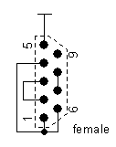 the GUI tried to read the COM port, the program crashed with a “Run time error 8020, Error reading comm device.” A search on internet revealed that this particular problem only occurres for USB to serial converters based on the “Prolific” chipset, and only under Windows Vista or Windows 7. Indeed I used a Sweex adapter based on the Prolific chip set. Fortunately, when I tried a Digitus DA-70157 USB to Serial adapter with an FTDI chip set it worked flawlessly.
 I would really appreciate it if some of you would take the effort of installing the GUI and mail me your experiences. Fortunately it is very easy to test the GUI and the communication of the GUI with the (emulated)
COM port, without having the actual uTracer hardware connected. Although
it is possible to test the GUI with the COM port just open, a more thorough check is possible if the COM port is fooled by connecting the transmit pin to the receive pin. The small dummy uTracer circuit on the right shows how such a circuit can be wired on a 9-pin female RS232 (DB9) connector. Pins 2 and 3 are the data pins. The other wiring makes sure that the handshake signals are properly bypassed.
I would really appreciate it if some of you would take the effort of installing the GUI and mail me your experiences. Fortunately it is very easy to test the GUI and the communication of the GUI with the (emulated)
COM port, without having the actual uTracer hardware connected. Although
it is possible to test the GUI with the COM port just open, a more thorough check is possible if the COM port is fooled by connecting the transmit pin to the receive pin. The small dummy uTracer circuit on the right shows how such a circuit can be wired on a 9-pin female RS232 (DB9) connector. Pins 2 and 3 are the data pins. The other wiring makes sure that the handshake signals are properly bypassed.
To test the GUI, first install it as described above. To have a 100% fail safe test, connect the “dummy uTracer” circuit to the COM port. Start the uTracer and click the “Debug” command button. Select the proper COM port number and press the “Ping” command button. Pressing the Ping button will cause the GUI to send two command strings to the uTracer. The first string is a <00> “start measurement sequence” command, and the second string is a <50> “read out all analog channels” command. When the COM port is open, the GUI will transmit the first character “0” and then wait for uTracer to echo this character. Since nothing is echoed it will detect a timeout and after 2 seconds and give a timeout error. When the dummy circuit is connected to the COM port, the GUI will successfully transmit the two command sequences and then after 10 seconds give a timeout error because it expects a result string to be send back by the uTracer. Both responses indicate that the GUI and the communication with the COM port function properly.
| to top of page | back to homepage | to part I |
I am aware of the fact that the picture to the left bears no relation to tubes or tube testers whatsoever. It is simply there to remind me later of the nice 2012 summer holiday we had in Julianadorp
 near Den Helder in the the very North of Holland, and of the fact that most of the “free hours” there were spend on designing a PCB for the uTracer project. If you like flat-landscapes, wind, flowers, wide sand-beaches and very moderate temperatures, this is the place for you to spend your holiday. Being a Dutchman I am used to flat landscapes, however The flatness of this part of Holland is even for me overwhelming. There are many places where you can stand and have a 360 degree un-obstructed view of the horizon. Add to that fields filled with flowers and some of the widest sand beaches in Europe and you have a pretty amazing, but certainly not picturesque or tropical landscape which is particularly popular with our eastern neighbors.
Already several months ago I made up my mind to try to make a construction kit out of this project. There are several reasons why. First of all, quite a number of people have asked me to do so. I think the examples in one of the previous sections show what a versatile instrument the uTracer is, and what a satisfaction it gives to bring those old gems back to life. I would like to offer others, who cannot afford the more expensive testers which are on the market, the same experience. The second reason is that I would like to experience what it takes to bring something like this to the market, be it even on a very small scale. I have worked my whole life in research, and as such have none or very little experience in what it takes to really sell something that I have made. I have an endless admiration for entrepreneurs and I would like to be one, but I don’t think I have the right genes. So here was the opportunity to be a small scale entrepreneur and I decided to go for it, not to get rich, but just for the experience.
For all the other projects on my web pages I have always offered all the soft- and firm-ware for download. Just to protect this project from being copied too easily, I decided in this case not to give away the micro-controller firmware. So what I intend to offer for sale are: 1. The programmed PIC controller for a small fee to cover expenses, for people who want to construct their own uTracer (and there are already a number of people doing that!) 2. A complete kit including PCB, all components and the programmed PIC micro-controller. Not to be included are the power supply and tube sockets etc. The utracer was designed to operate from and old 18-22 V laptop power supply chord. Most people have an old power chord lying around, and if not, it should be possible to buy one for practically nothing at flea markets, booth sales or the internet. Also not included are a case, tube sockets, electrode switches etc. I found that most people interested in the uTracer have these part lying around and have very distinct preferences with respect to the mechanical construction anyway.
My “plan de champagne” to come from a perfboard prototype towards something that can be sold comprises four steps:
After talking to “some of the people in the field,” I decided to design the PCB using Eagle. Eagle seems to be a kind of standard, at least for amateurs, and a number of PCB vendors have endorsed Eagle as a preferred file format, next to the Gerber standard. On top of that Eagle is for free for small PCBs and moderately priced for commercial use. As mentioned before I never designed a PCB in my life and found it quite an adventure to start with it. What I found to be a great help starting with Eagle and PCB design in general where the “PCB Design Tutorial” by David Jones, the “Eagle 5 Tutorial” from Cadsoft, and a great series of YouTube tutorials made and uploaded by Jason from rpcelectronics. I decided not to enter the schematic first in Eagle, but to directly layout the PCB. Of course I had the perfboard with the component placement already pretty much optimized for shortest connections and minimal crossings. Being used to CAD tools for designing ICs, getting started with Eagle was not too difficult. The program works pretty fine, and only has a few minor irritation points.
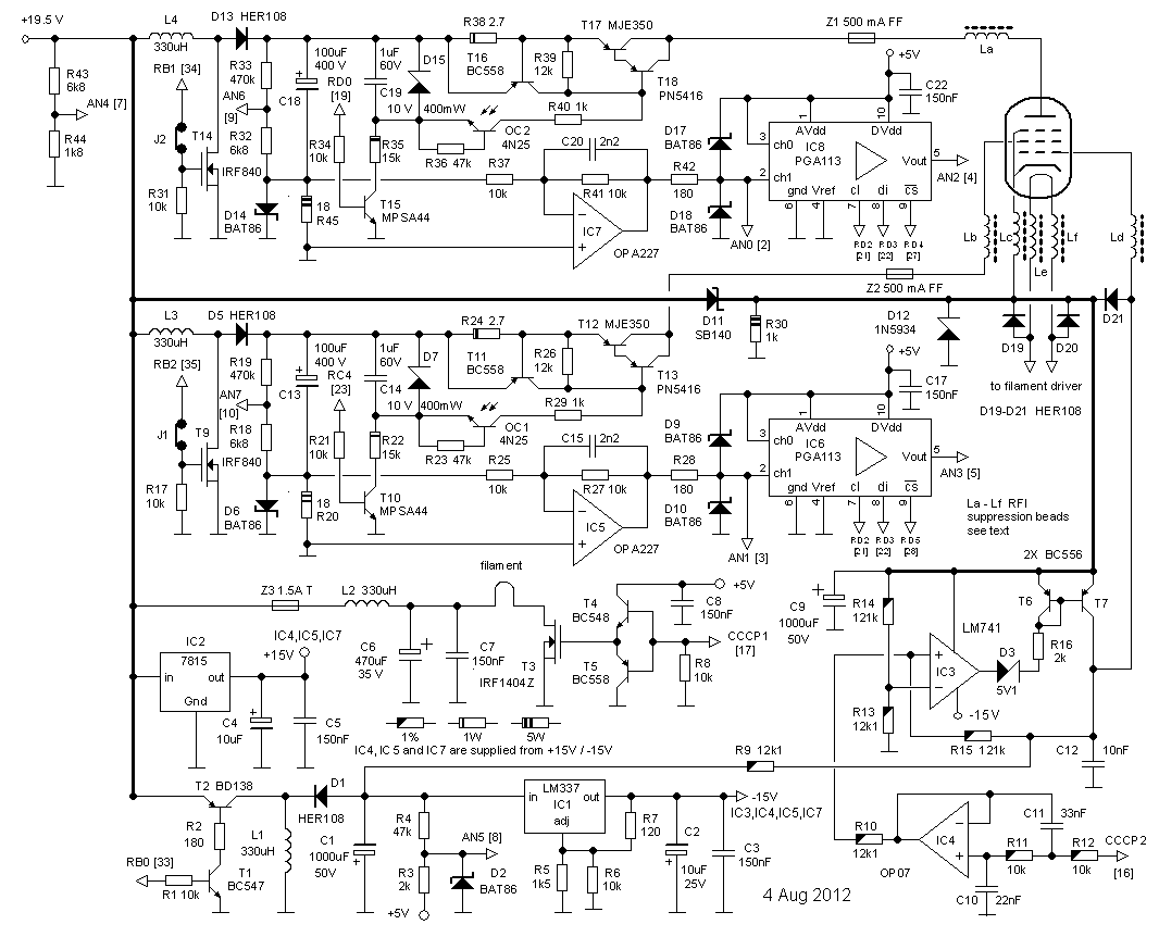
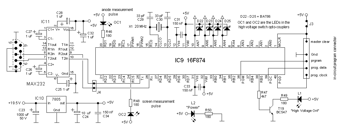
Figure 20.1 Updated circuit diagram with component numbering consistent with text on PCB
The PCB manufacturer I selected was Eurocircuits which is located in Belgium. They are the supplier of PCBs for the magazine Elektor, and also a few colleagues gave a good reference. I think they are quite cheap. A 10x16 cm prototype PCB costs around 60 euro and for larger quantities the price obviously drops. It can be that there are Chinese vendors who can make them for a few euro cheaper, but then again I am a strong believer in supporting the local economy. The site of Eurocircuits is full of technical information (although not that clearly structured) and even offers Eagle technology files (.dru) for download, so that the PCB can be designed directly in their technology.
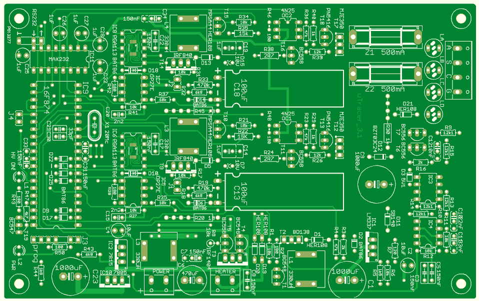
Figure 20.2 Impression of the PCB as you get it returned by Eurocircuits after they have verified your PCB.
Designing the PCB was actually a very nice relaxing job to do. It also gave me a good opportunity to compare the uTracer schematic versus the hardware that was actually on the table. I found a number of relatively small discrepancies, and the corrected circuit diagram is shown in Fig. 20.1. As mentioned before, the prototype circuit on the perfboard was already pretty much optimized with respect to component placement. For practical reasons I wanted to stick as closely as possible to the eurocard format (10x16 cm). This means that the board is rather full and that there was no place for the RS232 connector, the heater RFI chokes and fuses. Personally I do not think that that is such a big deal since I guess that most people have their own ideas on where to locate those. The end result is rather nice, and I cannot resist showing of with it (Fig. 20.2)
Although Eurocircuits directly accepts Eagle (.brd) files, I preferred to convert the design to Gerber myself. The reason is that default Eurocircuits uses only the component names and outline for the silk-screen. I wanted to have also the component values included. Converting the design data to a Gerber file is very easy. Eurocircuits has a very informative series of articles on their site about these topics which includes a detailed description of how to convert Eagle designs to Gerber. A very useful tool to check the Gerber and Excellon is the 3-D Gerber viewer from Mayhew Labs.
The next step was to find a suitable supplier. As mentioned before, I usually build my projects from what I have “on stock,” so I have never
actually ordered any parts from a supplier. I considered four candidates:
Farnell, Mouser, Reichelt, and Conrad. Farnell has the largest assortment, but is expensive and is not really too keen on supplying to individuals.
 Individuals have to Fax/mail a component list and above 50 euro they do not charge shipping costs. Conrad, I discovered, has a somewhat limited assortment compared to the other three. Reichelt is very cheap, but charges 12.50 euro shipping costs outside Germany. Mouser is very cheap and for orders above 65 euro charge no shipping costs (under 65 euro they charge 20 euro !). In the end I selected Mouser, one of the reasons being that they are located “around the corner” in Eindhoven.
Composing the Bill of Materials (BOM) I discovered that some components I used in the prototype were really very hard to get. The BF487 high voltage transistor was easily replaced by an MPSA44. The OP27E proved more difficult. The OP27E combines a very low offset voltage (10 uV) with a reasonable slewrate (3 V/us). In the end I decided to go for an OPA227 (typically 5 uV offset, 2.3 V/us). If there is ever going to be an uTracer Version 4, than replacing the older dual supply voltage OpAmps for modern single supply types is high on my list. As an alternative for the MC34071 I will try an OP07. In the prototype I used DR125-331 inductors from Coiltronics. They are rated at 1 Amp. Instead I decided to go for the DR127-331 which is rated for 2A, has the same footprint but is twice as high (and heavy). This will allow me to go to longer pulses and thus faster charging of the high voltage capacitors. I didn’t select an alternative for the PN5416, sorry. I have a few thousand of them lying around and they are excellently suited for the job. Mouser didn’t have a BZT 03C24 on stock at this moment, so I ordered a 1N5934 instead. Finally, the CNY47 optocoupler appeared to be obsolete. Comparing datasheets I decided that the 4N25 should be a good alternative. This is something I will have to check in the prototype circuit. Especially a fast switch-off characteristic is important for correct functioning of the compliance protection.
In the mean time the parts for a “test-kit-version” uTracer have arrived in an enormous plastic bag in which each component was almost individually packed in another plastic bag. I think all the profit must have gone up in all these nice zipper bags. I will re-use them for the kits! It felt rather silly ordering all those components while I have almost all of them lying around, but I wanted to be absolutely sure that the part numbers and the parts I selected are both electrically ok and will fit on the PCB. So at the moment I am waiting for the PCB which will arrive in a few days. When it arrives, I will build up a uTracer from scratch, see what issues I encounter, and at the same time compile a construction manual. In the mean time a number of people have already started building their own uTracer even without the PCB! The first one is ready now, and functioning - apart from a few minor issues – as expected!
| to top of page | back to homepage | to part I |
At the moment of writing of these words about 80 uTracer kits have found their way over the world, and I thought it was a good moment to reflect back on the past 4 months and to write a few words about it for posterity.
The first ten kits were really exciting. After building the first prototype, I was reasonably confident that the kit could be built without too many difficulties, but nevertheless, I thought it was quite a big step to just send people a bunch of parts and a building description in the hope they could reproduce the original! After all, people pay quite a lot of money for the kit, and I really would like to avoid disappointments.
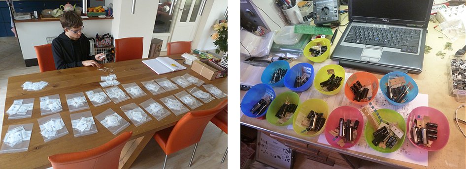
Figure 21.1 Sorting the components required more time and organizing than expected. My son Daan earns some pocket money helping to sort the resistors.
It all turned out quite nicely I am happy to report! The first uTracers worked perfectly without any serious problems. There were some minor issues: in the first series two 470 k resistors and a few 150 nF decoupling capacitors were missing. A small fault in my “Bill-of-Materials” that was easily corrected, and the missing parts were supplied to the buyers of the first series by regular mail. A bit more annoying was a problem related to the GUI. In some countries such as Holland, Germany, Finland, the decimal delimiter symbol is not a period (“.”) but a comma (“,”). When Windows is installed on a computer, the language setting will determine what delimiter symbol is used. However, it appears that when writing a decimal number to a file, Visual Basic will use the symbol set by the language, but when reading it, it will always expect a period! Since I use the English version of Windows, I never noticed the problem, but people with a Dutch, German or Finnish version of Windows experienced problems with the calibration file. The matter can be resolved by tweaking the calibration file by hand, or manually changing the delimiter symbol in Windows. A more permanent solution was the release of a new version of the GUI which contains a special input parser, although strangely enough the problem tends to persist in some cases in Finland!?
I decided open “Bugs and Issues” page to communicate as openly as possible these issues and their fixes.
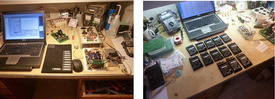
Figure 21.2 Each PIC processor is programmed and tested in the breadboard version of the uTracer 3. Testing is done on a EL84.
I decided to “fabricate” the kits in series of 20 to 30. Since quite a lot of money is involved in ordering the PCBs and the components, the customers of the first three series had to wait until enough orders and payments had been collected so that I could order the parts. In the mean time I have gained so much confidence in the project, that I try to keep a number of uTracers on stock so that I can ship immediately. Ordering components for a new series is always a bit of a hassle. I order most of the components from Mouser. I have an excel sheet with all the components and their Mouser order numbers; I only have to enter the number of kits, and then excel generates a file that can be directly uploaded to Mouser. That is usually the moment when the aggravation starts: very often a components appears not to be on stock, and the search for a replacement type has to start. That is not always easy and sometimes a risk as we will see later on. The pitfall is to stock components when they are available. In the mean time I now also have a Farnell account so that I can use them as second source, but most of the time they are more expensive. A continuous problem is the MPSA44 transistor which is only available from Farnell. One of these days I think I will redesign the PCB for a more easily available HV npn. By the way, ordering the PCBs from Euro Circuits is always a pleasure: just click for a repeat order and the number of PCBs and that’s it, no credit card just an invoice after delivery and always perfect quality!
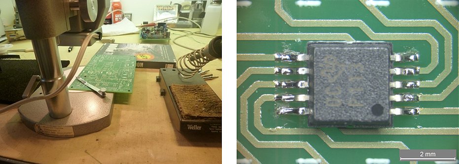
Figure 21.3 The soldering of the SSOP package of the PGA113 is done using a small Olympus stereo microscope. After a bit of practice it is relatively easy.
After the components and the PCBs have arrived the assembly of the kits starts. Even though I now have developed quite a routine, it always consumes nearly all my spare time for the better part of a week. To make the kit as “fool-proof” as possible, I decided to put all the components which could cause confusion (resistors with color codes, diodes with impossible small imprint, etc) in separately labeled bags. It is quite some extra work, but highly appreciated by the customers. Sometimes the kids help a bit to earn some extra pocket money. I usually start with the resistors which take most of the time. Next, the PIC processors are programmed individually. Before they receive their label all processors are tested by measuring a set of curves of an EL84. Next the capacitors, diodes/transistors and miscellaneous components are sorted. The photographs give an impression of this process.
I tried to use as much as possible though-hole components for the uTracer. Most amateurs (including me) have a bit of an aversion to SMD components, but unfortunately through-hole components are rapidly becoming obsolete, and more and more new, and often very interesting ICs are only produced in SMD packages. The PGA113 is one of those ICs; it turns the uTracer into a real measurement device, but comes in an incredibly small MSOP-10 package with a lead pitch of 0.5 mm. Not everybody has a microscope and a pencil solder-iron or the steady hand and experience to handle these devices, so I decided to supply the PCBs with the PGA already soldered on it. After about 80 boards I am now quite experienced and can solder two PGAs to a PCB in about 12 minutes (I timed it!). After soldering of the PGAs the PCB are packaged in ESD-safe bags which are recycled from my Mouser deliveries.

Figure 21.4 The CFO “Chief Financial Officer” and the packaging and shipment department!
I am absolutely chaotic when it comes to administration and finances so I was very fortunate that my wife - Marie-José - stepped in as “Chief Financial Officer (CFO)”. After people have sent me a first email indicating that they are interested in buying a uTracer, I transfer them to my CFO. Apart from the administration and the finances, Marie-José also takes care of the shipment. Fortunately, the whole uTracer kit nicely fits in a “post box box” ( a box with a size that fits in a letter box). Shipping the uTracers this way is relatively cheap and it also greatly reduces the formalities needed for customs. In the village where we live the post office has been reduced to a post-office agency, operated by the local super market staff. It is always amusing to hear the stories of my wife about the confusion these packages with destinations all over the world cause! It is not often that people our village ship packages to: Canada, South Korea, Singapore, or Moscow!
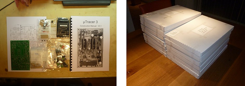
Figure 21.5 The contents of the Kit and Kits ready to be posted.
All in all the uTracer business has been most rewarding. It is really fun to sell something you have made and get enthusiastic feedback from customers all over the world. It has brought me in contact with a lot of very interesting people! The only “complaint” I frequently get is that the voltage ranges are a bit low. Especially people working on high-end audio power amplifiers would have liked to see somewhat higher voltages. Some people were even a bit angry that I - having gone through so much trouble to make the uTracer3 - didn’t take the additional effort to design it for voltages up to 400-500 V. In conclusion, the whole project was so much fun that I have started thinking (and even started experiments) on a uTracer4. Together with some very clever readers of my pages there are some ideas to extend the voltage ranges of the uTracer. If they work only time and many experiments will tell, and even then I am not sure if there will ever be a Tracer4 kit. The whole “family business” has cost me much more time than I ever could have imagined, and after all I also have a normal daytime job!
| to top of page | back to homepage | to part I |
 Most of the people who regularly read my pages will by now have recognized my passion for the “Sherlock Holmes.” Absolute fantastic reading! One of the great things about a private web-site compared to scientific papers and magazine articles is that you can publish exactly as you like, without having to bother about editors, reviewers or even worse, ones boss! Readers will therefore hopefully forgive me for making some allusions from time to time to that great adventure series.
A week ago somebody send me his uTracer because there was a problem that was difficult to solve by email. Something must have gone terribly wrong because the high voltage pnp transistors in one of the high voltage switches as well as one of the diodes across the 18 ohm sense resistors were defect. The damage was quickly repaired, but when I tested the circuit I noticed something different. The measurements were notably slow, especially for higher voltages. Compared to my own reference versions of the uTracer, the difference in speed could amount to 50% or more!
The problem obviously had to be found in the boost converter circuits which had never given any problems so far. The first suspect was the UF1J diode that I use as a replacement for the HER108. Replacing the UF1J for an HER108 didn’t make any difference however. The next, but unlikely, candidate was the IRF840 high-voltage NMOS transistor. In my own versions of the uTracer, as well as in the uTracers of first series, I used IRF840 transistors from and old stock I had made by International Rectifier. After the first series I ran out of transistors and had to order new transistors from Mouser, they were made by Vishay. Could it be that there was a difference between the original and replacement type? Replacing the Vishay transistor for an original International Rectifier type proved that to be so. The difference in speed is sometimes more than a factor 2!
At about the same time a Nick Barton who reported that he sometimes had a “time-out error” when he measured tubes at voltages up to 300 V. A time-out occurs when the GUI does not receive any data back from the uTracer within 10 seconds after a measurement command is issued. So as it happened I could directly tell him the cause of the problem. In the email conversation that followed he recommended me the SPU07N60C3 from Infineon. It has a lower and more tightly specked Vt (threshold voltage), a lower Ron and also lower capacitances. It seemed like an excellent choice and I immediately ordered a few, and indeed they performed equal or even slightly better than the original IRF840s.
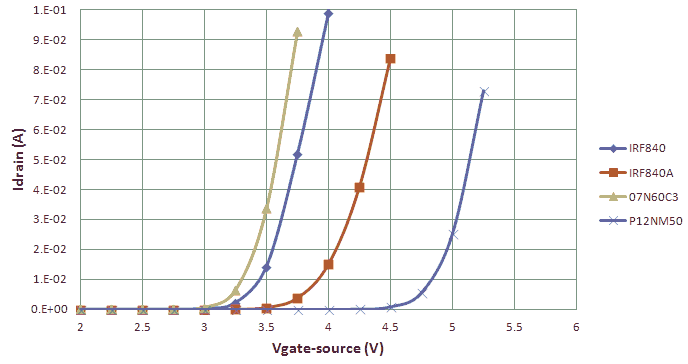
Figure 22.1 Drain current versus gate-source voltage for different HV MOSFETs measured on a Keithly 4200.
To find the difference between the different transistors, their Id-Vgs (drain current as a function of gate-source voltage) was measured on a Keithly 4200 parameter analyzer with the help of my colleague Johan Klootwijk. For comparison also an STP12NM50 high-voltage MOSFET from ST was included in the test. In the uTracer this transistor resulted in extremely slow measurements. For a proper functioning of the uTracer, the MOSFET should be able to drain about 1 Amp of current, at a gate-source voltage of 5 V. Unfortunately, the upper current level of the Keithly parameter analyzer is limited to 100 mA (it is designed to test submicron IC transistors), but at least this lower part of the curve should give a good idea of the trend at higher currents.
The measurement results are shown in Fig. 22.1. The STP12NM50 has the highest Vt of the four transistors and hence the lowest current at any given gate voltage. The difference between the IRF840 and the IRF840A is quite pronounced, almost half a volt in threshold voltage resulting in about a factor of ten lower drain current for a given gate voltage. Indeed the SPU07N60C3 performed best with even a slightly lower Vt than then the original IRF840 and a somewhat higher transconductance. Indeed a very good replacement. Needless to say that I ordered a new set of SPU07N60C3 transistors which will be send to all the owners of a series two or three uTracer.

Figure 22.2 Replacement MOSFETs ready to be posted
| to top of page | back to homepage | to part I |
Recently I received a number of questions from people who have questions or issues related to the power supply of the heater, especially in combination with directly heated, very low voltage (<4 V), high current filaments. Let me start by explaining that the heater supply was originally designed with the more ordinary 6.3 – 12 V radio/television type of tubes in mind. For these kind of tubes there is no issue, but especially the low voltage / high current combination pushes the supply to the limits of its performance. Also it is not clear to everybody how directly heated tubes should be connected.
How does it work.
Let’s first start with recapitulating how the heater supply works. The temperature of the heater, and thus the emission, is a function of the amount of energy which is dissipated in it. Furthermore, the heater is basically a resistive load with a large thermal constant. In the uTracer these properties are used to realize a very simple supply circuit. In its simplest representation it is nothing more than a power MOSFET with a very low on resistance which directly connects the 19.5 V power supply to the heater. The MOSFET is driven with a 19.5 kHz signal with a variable duty-cycle (Fig. 23.1A). The switching frequency is so fast that the temperature of the filament cannot follow the variations, and in this way assumes a temperature which relates to the average dissipated power. By varying the duty-cycle, the amount of power dissipated in the heater can be varied. The relation between the duty-cycle, the set point heater voltage, and the supply voltage is derived here. Note that the duty-cycle is equal to square of the ratio of the set point voltage to the power supply voltage (more here)! So if a heater is specified for 10 V and the power supply voltage is 20 V, the duty-cycle has to be set to (10/20)^2=(0.5)^2=0.25 or 25%!
Some people try to check the heater supply voltage of the uTracer with a normal voltmeter and find very strange values. That is because the output of the heater supply is pulsed. You cannot check the heater supply voltage of the uTracer using an ordinary voltmeter! Only a voltmeter which can measure the true rms (Root Mean Square) value of an AC signal with a sufficiently high bandwidth can be used. I even don’t have such a voltmeter, but a few people have reported on it (Link1, Link2).
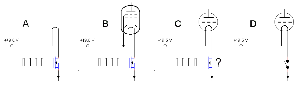
Figure 23.1 Principle of the heater supply
The heater supply in the uTracer obviously cannot be floating and has to be connected to the rest of the circuit. Figure 23.1 shows the principle of how that is done. Since the output voltage of a boost converter can never be lower than the supply voltage, the cathode of the tube is referenced to the positive supply voltage (more here). For indirectly heated tubes this obviously is no problem at all (Fig. 23.1B). For directly heated tubes there seems to be a problem because here the heater also serves as cathode, and what is now the cathode potential when the heater is switching on- and off all the time between zero and the maximum supply voltage (Fig. 23.1C)? The solution is simple, during the 1 ms measurement pulse when the high voltages are applied to the tube, the heater supply is completely switched off so that the whole filament is at ground potential (Fig. 23.1D)! Note that this is a rather strange situation normally never occurring in any practical circuit using directly heated tubes. In normal circuits the heater voltage will always cause a voltage gradient along the filament resulting in a gradient of the grid-heater bias. So the currents in a real circuit will differ slightly from the currents measured with the uTracer! How serious that is depends on the heater voltage and the grid bias.
Low Voltages, High Currents.
As mentioned before some people have reported problems for tubes with a low-voltage/high-current heater. Let’s take as an example an imaginary tube with a 2.5 V / 1.0 A filament. The heater resistance of such a tube is 2.5 ohm in heated state. The cold resistance can even be up to a factor 10 lower! This means that when the MOSFET switch is closed, the current will be at least 20/2.5 = 8 A, and even much higher during start-up! But for how long is the MOSFET switch closed? Remember that the duty-cycle is given by d = (Vfil/Vsupl)^2, so d = (2.5/20)^2 = 0.016 so only 1.6%. The frequency of the PWM signal is 19.5 kHz so the period time is 1 / 19500 = 50 us, 1.6% of that is 0.8 us. In that short time the current has to rise to 8 A. Is that realistic? There are always inductances in the circuit which resist against a rapid increase of current.
How much inductance can we tolerate? Let’s try to make a simple back on the envelope calculation. When a DC voltage is applied over an inductor, the current increases linearly with time according to I = V*t/L. So assume that we have a pulse of 0.8 us, a supply voltage of 20 V, what inductance causes the current just to increase to 8 A within that 0.8 us? L = V*t/I = 20*0.8us/8 = 2 uH. So already for inductances larger than that, the heater circuit does not function properly anymore for this imaginary tube! Note that for higher heater voltages there is no problem at all. A 6.3 V / 1.5 A heater of an EL34 works perfectly, the problem is in the combination low-voltage and high-current.
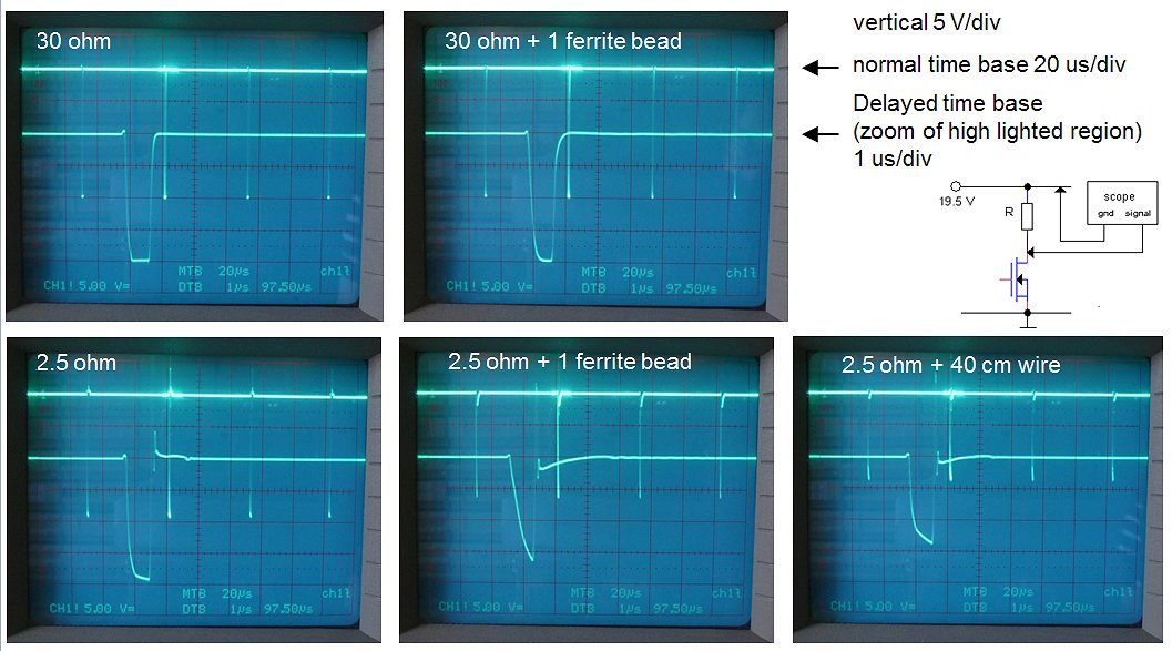
Figure 23.2 Heater supply under various load conditions. The heater voltage was set to 2.5 V (Fig. 23.4). The upper trace in each photo shows the realtime output signal of the heater supply, the lower trace shows a magnification of the pulse (1 us/div).
To demonstrate what is going on, I replaced the imaginary tube of the example with a resistor which was connected directly to the heater terminals on the PCB to minimize stray inductances (Fig. 23.4). The current through the resistor was measured by measuring the voltage drop over it (Fig. 23.2). During the measurement, the ground of the oscilloscope was connected to the positive power supply, so that the on-state will appear as a dip in the trace. For the measurements I used the “delayed time base” option on my good old analog scope. The heater voltage was set to 2.5 V. First a 30 ohm resistor was connected. In that case the current is very low, and the current pulse is almost ideally rectangular. Note the very narrow pulse width (0.8 us) which ideally will result in 2.5 V RMS in the resistor. Adding a ferrite bead in series with the resistor changes the pulse a bit, but not dramatically. Next, a 2.5 ohm resistor was connected directly to the terminals. Even in this case, with peak currents up to 8A, the pulse is still nearly ideal. However, adding even a single ferrite bead complete distorts the current pulse. The inductance of the ferrite bead supplied with the kit (5.7 uH) causes a linear increase in current which not even reaches its final value before the end of the pulse. In this situation obviously too little power is delivered to the resistor. Even when a piece of 40 cm wire is added in series with the resistor, the inductance of the wire is already so high that the current pulse is seriously affected.
In this measurement a resistor was used which has a more or less constant resistance. However, the heater of a tube can have in its cold state a resistance which can be a factor ten lower compared to its nominal on-state resistance. So if this would have been a tube instead of a resistor it could have been very likely that the amount of power delivered to the tube during heating would have been so small that the tube never would have heated at all!
Obviously this type of circuit is not suitable for these very “heavy” heater tubes. One of the things on the “to do” list to look into is the possibility of a buck-converter for the heater. In the meantime, several measures can be taken to minimize the problem:
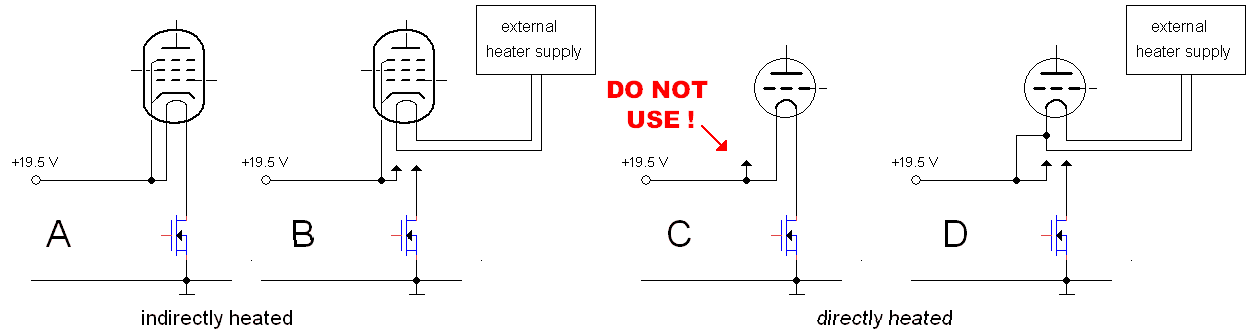
Figure 23.3 Connection diagram of indirectly / directly heated tubes with internal / external power suppies.
Testing Indirectly Heated Tubes
To test an indirectly heated tube with the uTracer connect the heater and the cathode of the tube to the corresponding connections of the uTracer (Fig. 23.3A). If you want to use an external heater supply, you can simply connect the heater of the tube to the external supply. The cathode of the tube obviously remains connected to the uTracer (Fig. 23.3B).
Testing Directly Heated Tubes
To test a directly heated tube you again connect the heater of the tube to the heater connections of the uTracer, but in this case the cathode connection on the uTracer is not used (Fig. 23.3C)! Connecting the cathode connection to one of the heater connections can short-circuit the heater supply, which in one case destroyed a complete uTracer, DON’T DO IT!
The situation is different when an external heater supply is used which is electrically floating with respect to the uTracer. In that case the cathode connection has to be connected to one of the heater connections on the tube (Fig. 23.2D). The curves may vary depending on which heater connection is connected to the cathode, due to asymmetries in the tube. You may even consider placing a low-resistivity potentiometer in parallel to the heater with the slider connected to the cathode connection.
Another note of caution is needed when delicate battery tubes are measured! As explained before, the heater duty-cycle becomes very short for low heater voltages. Small variations in the duty-cycle will thus result in relatively large variations is the dissipated power. So when I measure delicate battery tubes like the DAF96 (1AH5), Russian pencil-tubes etc, I simply use a 1.5 V battery as heater supply, In that way nothing can go wrong whatsoever.
A Simple Calibration Procedure
A simple trick to compensate for the inductances in the circuit is just to increase the set-point value of the heater voltage until the proper heater temperature is reached! The question is how much the heater voltage has to be increased? Unfortunately that differs from tube to tube, and since everything so very much depends on stray inductances, even from uTracer to uTracer. If it is your plan to test only a limited number of different types of tube, the following calibration procedure can be followed:
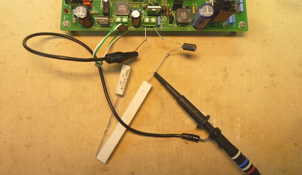
Figure 23.4 Testing of the heater supply
| to top of page | back to homepage | to part I |
The heater supply continues to be a topic of much discussion and questions. I thought that I had written the final words about the matter when I received an email from Ron Soyland. Most of us will probably have seen one or more of the fantastic videos Ron has uploaded to YouTube under the name “glasslinger.” Ron actually makes his own vacuum tubes! Really fantastic is his series of videos on the re-construction of a spherical Lee de Forest audion tube. As Ron explains in his videos, the heater voltage of his tubes varies between 1 and 3 V at a current of 2 to 4 Amps, depending on the length of the heater. Ron sent me an email with the question of the uTracer could be used to measure the emission of the tube as a function of heater voltage, so anode voltage constant and sweep heater voltage. Actually there is a built in function in the GUI which allows for exactly that measurement, but in the previous section I explained that the present design has a problem with exactly the combination of low voltage and high current filaments!
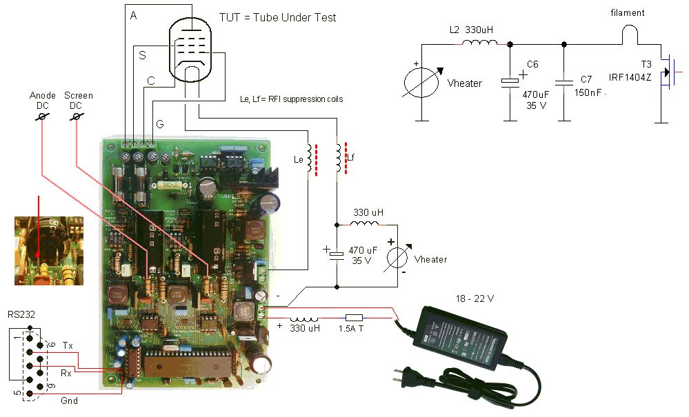
Figure 24.1 Connection diagram for the low-voltage external heater
In the previous section it is explained that this problem is caused because the supply voltage of the uTracer is rather high (19.5 V). For low heater voltages this results in a very low duty-cycle of the PWM heater voltage which, in combination with inductances in the circuit and the high currents, causes the problems. My simple solution was to use an external heater supply. This however, makes it impossible to do an automatic heater voltage sweep. After thinking about Ron’s question it occurred to me that there is a kind of compromise solution. The trick is to use the external heater supply to feed the heater PWM circuit, and to set this supply voltage to a voltage as low as possible. So, for instance, if Ron wants to make a sweep from 0 to 4 V, the heater supply voltage should be set to something like 4.5 V. In this way the pulses of the PWM modulated heater voltage do not become too short. Obviously this will require a modification of the GUI software because normally the 19.5 V supply voltage of the uTracer is taken as a reference.
Figure 24.1 explains the idea. The insert shows the heater circuit of the uTracer. Instead of using the 19.5 V supply voltage for the heater circuit, in this case an external power supply is used. The “floor plan” shows how with an extra inductor and a capacitor, the modification can be implemented without modifying the PCB. With a switch it is even possible to switch between the internal and the external heater supply. For the inductor any high current inductor of a few hundred uH can be used, e.g. one salvaged from an old PC power supply.
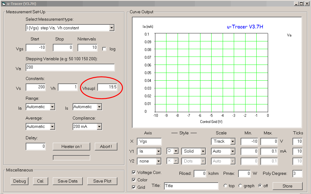
Figure 24.1 Main form of the adapted GUI (based on V3p7). Encircled is the field where the voltage of the external heater supply can be entered.
Also a small modification to the GUI was required to make the trick work. Figure 24.2 shows that a new field (“Vhsupl”) has been added to the measurement section of the main form. In this field the voltage of the external heater supply can be specified. The actual heater voltage specified in the field “Vh” can now be set to any value between 0 and Vhsupl. If now under “Select Measurement type” a heater sweep is selected (I(Vh)), the heater voltage can be swept from 0 to maximal Vhsupl. To avoid disasters if accidentally the user forgets to set heater voltage to the correct value, the default values of Vh and Vhsupl have been set to the safe values of 1 and 19.5 V respectively.
The adapted GUI can be downloaded here: V3p7H (compatible with GUI version 3p7), V3p8H (compatible with GUI version 3p8). This zip file only contains the exe file. I recommend to download and test the hardware first using the complete package from the download page. This will install all the necessary Active-X components (if you are lucky). The adapted V3p7H test GUI can be simply un-zipped and executed. Any feedback, bug reports etc. are welcome.
Michael Watterson was so attentive to point me to an error! Since in the uTracer the tube voltages (anode, screen and grid) are referenced to the positive power supply instead of ground, this trick does not work properly for directly heated tubes! I think that with an additional transistor it can be fixed. Nevertheless, it should work fine for indirectly heated tubes.
| to top of page | back to homepage | to part I |
From time to time I’m being asked if the uTracer is also suitable for testing tubes at positive grid biases. I have to admit that I never realized that there are circuits where the grid becomes positive during a certain phase of the signal and that there are tubes especially designed to operate in this regime. Certain types of class-B audio amplifiers and most class-B and class-C high-power RF transmitters work in this mode, so testing tubes in this regime is obviously of interest. The problem is that when the grid becomes positive, it starts act as a kind of anode, attracting electrons. As a result a grid current will start to flow and the grid will start to dissipate!
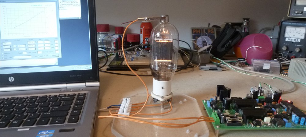
Figure 25.1 TZ-40 being tested for positive grid biases.
The grid bias circuit of the uTracer is designed for negative grid biases only. Some people have suggested “fooling” the circuit by adding a positive floating voltage source in series with the grid terminal so that e.g. the range of -50 to 0 V is shifted to -25 to 25 V (using a 50 V battery). Unfortunately this doesn’t work since the grid bias circuit is also not capable of delivering the substantial currents which would flow to the grid for positive biases. Note, by the way, that this trick does work to extend the grid bias range of the uTracer towards more negative biases (read more)!
This was the situation until James Hill on the Audio-Talk forum had the fantastic idea of using the screen supply to
drive the grid for positive biases! Why didn’t I think of that before, how stupid can you be! The idea is indeed brilliant! The screen supply is
 capable of delivering positive grid bias pulses and what is more
important: capable of accurately measuring the resulting grid current.
Another important, and even necessary feature is that in this way the grid bias is pulsed so that the excessive dissipation in the grid, which would occur if DC biases were used, is prevented. So far as I could see, the idea only had two problems: The first one was that the GUI software
didn’t provide for such a measurement. The second one was that the screen, as well as the anode supply loos a bit of accuracy for low voltage due to the limited resolution of the AD converter and the principle behind the circuit. Finally, needless to say, since there is only one screen supply the method is only suitable for testing triodes.
capable of delivering positive grid bias pulses and what is more
important: capable of accurately measuring the resulting grid current.
Another important, and even necessary feature is that in this way the grid bias is pulsed so that the excessive dissipation in the grid, which would occur if DC biases were used, is prevented. So far as I could see, the idea only had two problems: The first one was that the GUI software
didn’t provide for such a measurement. The second one was that the screen, as well as the anode supply loos a bit of accuracy for low voltage due to the limited resolution of the AD converter and the principle behind the circuit. Finally, needless to say, since there is only one screen supply the method is only suitable for testing triodes.
The first problem was easily remedied. Since I was working on a new release of the GUI anyway, the two new measurement types could easily be implemented in version 3p8. Two new measurement types were implemented to allow for I(Vg) and I(Va) measurements in positive grid bias mode (+Vg mode). In the “+Vg mode” the grid is connected to the screen terminal of the uTracer. The normal grid bias output is working (constant voltage), but in most cases not used. Note that for the “+Vg mode” measurements in the measurement type select box (screen capture left), “Vs” is used to denote the grid connection. I thought this more logical since the grid of the tube has to be connected to the screen pulse output of the uTracer. Also In the graph “+Vg” has replaced Vg. The only thing that was rather hard to change was the axis-name for the grid current. So for these two measurements Is represents the grid current, sorry for that!
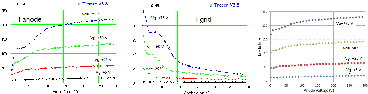
Figure 25.2 Anode current (left), grid current (middle) and sum of grid and anode current (right) as a function of anode voltage for a TZ-40 under positive grid bias.
So time ago a friend gave me a beautiful vintage pre-WWII Taylor TZ-40 triode (Fig. 25.1). I want to use it to test my circuits ideas for the uTracer4. The TZ-40 is especially suitable for this since it is specified to at least a 1500 V anode voltage, anode currents up to several hundreds of mA in combination with negative and
 positive grid biases. The TZ-40 is quite a sizeable directly heated triode with a graphite anode. It is designed for class-B audio ( 250W a pair) or class-C RF (200W) applications. Since the tube is designed for (near) zero bias applications, the grid is positive during a large part of the phase of the signal. The datasheet therefore specifies the anode and grid currents for grid bias values up to 200 V!
Using the screen supply to drive the grid and the new measurement types of the version 3p8 GUI the TZ-40 was measured in positive grid bias mode (Fig. 25.2). Similar to the datasheet curves, the anode current curves surprisingly resemble tetrode curves, probably because – just as in the case of a tetrode – the anode is to some extend shielded by the constant potential of the control grid. Similar to tetrodes, the curves exhibit a kind of kink for low anode voltages. In contrast to tetrodes this kink is not caused by secondary electrons emitted from the anode, but just by electrons which are being taken up by the positive control grid, especially when the voltage on the anode is lower than the voltage of the control grid. As soon as the anode voltage increases above the control grid voltage, most electrons are collected by the anode, and the grid current shows a sharp decrease. Note that the pulsed measurement method used in the uTracer is really allowing us, perhaps for the first time, to take these characteristics because under DC conditions the grid is easily damaged for grid currents in excess of a few tens of milliamps (they are also not shown in the Taylor datasheet). Although it has (I think) little electronic interest, I added the grid current to the anode current to confirm that the grid current accounts for the “kink” in the anode current (Fig. 25.2 right). James Hill send be another example of a positive grid bias measurement (Fig. 25.3). In this case it was an 826 power RF transmitting triode, with an maximum anode dissipation of about 40W.
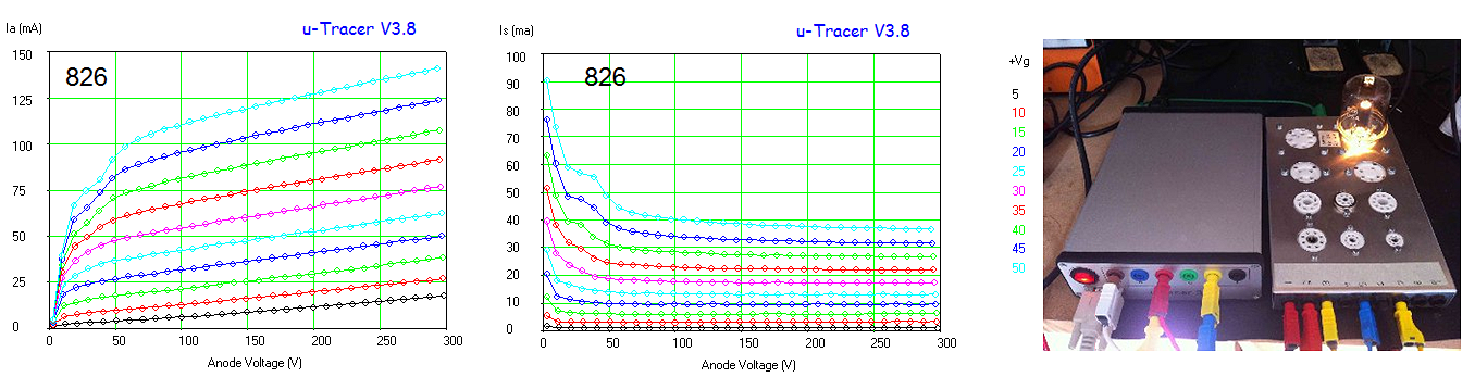
Figure 25.3 Anode- and Grid current of an 826 RF triode with positive grid bias (courtesy James Hill).
Noisy and Wobbly curves, and how to deal with them.
When James proposed to use the screen supply for positive grid biases, I was afraid that it would result in “noisy” curves. The reason was that I have the impression that both the anode, as well as the screen supply lose some accuracy for low voltages. There are two reasons for my suspicion. The first reason is that for low voltages the relative error of any AD converter increases. There is always an uncertainty of one LSB in this case corresponding to approximately 0.3 V. Add to that that there might be some noise in the reference voltages of the AD converter, and the total uncertainty of can easily amount to a volt or so. At 300 V this is a relatively small error; however, at say ten volts the error is enormous! The second source of noise can be found in the way the boost converters operate. Current pulses, four at a time, charge the reservoir capacitors until the required voltage is reached. Especially for low voltages, this can result in a small overshoot. Needless to say that when the screen supply is used to bias the grid that these small variations are amplified by the tube!
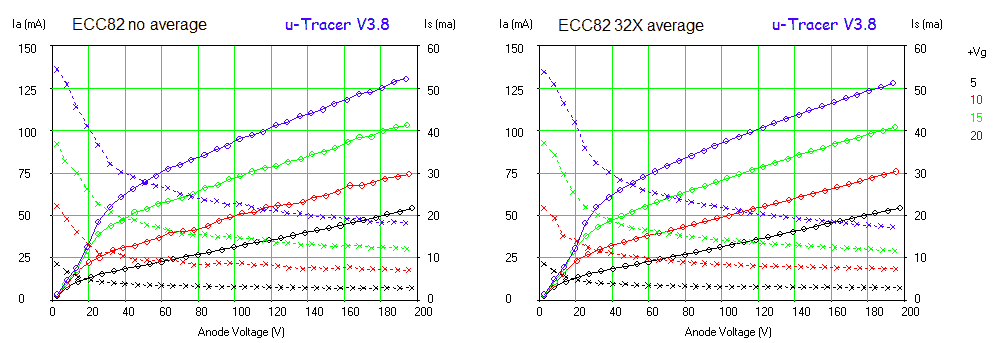
Figure 25.4 Eliminating noise from the curves by increasing the number of averages.
As it turned out, the problem was much less serious than I had feared. A nice indication that the anode and screen supplies are not that bad at all! The curves of Figs. 25.2 and 25.3 are actually quite nice and smooth. However, for very low grid voltages (Fig. 25.4 left) indeed some fluctuations can be observed. The most obvious method to reduce the fluctuations is to average the measurements. Normally the average feature of the uTracer is used to average out noise in the low current regime. When the averaging is set to automatic, the PIC automatically reduces the number of averages when the current that is measured increases. Figure 25.4 illustrates how manually setting the number of averages to some value higher than 1X can help to reduce noise in the curves caused by the “grid supply.”
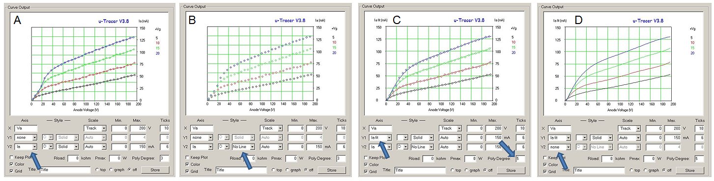
Figure 25.5 The straightening out of curves by means of polynomial fitting.
The curve-fitting function which is built-in in the GUI to produce noise free transconductance curves can also be used to straighten-out noisy or wobbly curves. Figure 25.5 illustrates how it is done. We start by first plotting the measured data along the second Y-axes (Fig. 25.5A). Next the solid lines are removed, leaving only the markers (Fig. 25.5B). We then select the fitted current to be displayed along the primary Y-axis, and the polynomial degree is set to such a value that a nice set of curves is obtained (Fig. 25.5C). Finally the markers belonging to the original measurement are also switched off (Fig. 25.5D).
Unfortunately it is not possible to combine in one graph positive and negative grid bias curves. However, Fig. 25.6 shows that by combining the data from several measurements in Excel, impressive graphs may be obtained. In this case an ECC82 was tested resulting in a set of curves that very few tube curve tracers could have produced without destroying the grid, or possibly the whole tube.
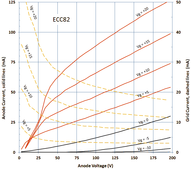
Figure 26.6 ECC82 measured with positive and negative grid biases.
| to top of page | back to homepage | to part I |
My first idea was to give this section the title ‘The singular case of the folded curve,’ and to write it in the form of a Shorlock Holmes / Watson dialog, but I am afraid that there not that many people out there who share my particular admiration for Conan Doyle and his writings, so I will limit myself to a more exact write-up. At the moment of the writing of this section some 160 uTracers have found their way to all continents (except Antarctica), and I take particular pride in the fact that, as far as I know, all of them are in good working order! Apart from a few minor problems, most problems encountered during the building and installation of the uTracer are related to the installation of the GUI and, if applicable, the USB-to-serial interface. Some tricks and tips collected from “the field” have been listed on the “Frequently asked Questions” page.
Assuming that “no news is good news,” I have to conclude from the very few problems that reach me, that the uTracer has proven itself to be rather reliable instrument. There have been however a few problems related to the high-voltage switch(es). Every design inevitable has a weak point, and I think that for the uTracer it is this part of the circuit. In the sixties and seventies the Dutch electronics magazine “Radio Bulletin” featured a column: “Ervaringen van een TV service monteur” (Experiences of a TV repair man). In this column an experienced TV repair man related of the more unusual cases he encountered on his rounds to people’s homes repairing televisions (and radios). What struck me as a child reading this column was how in 90% of the cases the repair was a routine job because a certain fault for a particular series of a certain brand in most cases pointed to this resistor or that capacitor; the weakest point in the design. It is funny that also with the uTracer I have now reached the stage that on hearing a problem, it has almost become a routine to pin-point the problem, or at least suggest a series of test which can isolate the fault.
Back to the high voltage switches. So far in four or five cases (I don’t remember exactly) a high voltage switch failed after a short circuit, or as a result of a very high current surge. That in itself is a bit disappointing because during the design of the uTracer I have done extensive testing to make sure it was short-circuit proof. At the end of this section I will speculate on the possible reasons why it can still sometimes fail. In this section I will first briefly recapitulate the working of the high voltage switches. Then I will review how you can diagnose that something is wrong, describe some tests you can do to isolate the problem, and finally I will end with a small speculation of why in practice the switches sometimes fail.
The high voltage switches, the essentials
Figure 26.1A Schematically shows the principle of the high voltage switch. A low-current boost converter charges reservoir capacitor C18 while diode D14 conducts. When the desired voltage is reached, the boost converter is switched off and for the next millisecond nothing happens to remove any noise or ringing from the circuit. Then the high voltage switch closes for exactly one millisecond. A current will start to flow causing a voltage drop over series resistor R45 (diode D14 is blocking now), which is measured by the processor. After another millisecond the switch opens again, and the voltage of the reservoir capacitor is measured again since the current will have discharged C18 to some extent.
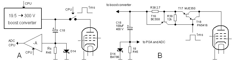
Figure 26.1 Block diagram and simplified circuit of the high-voltage switch.
What happens during a short circuit
When the output is short circuited, or when a very heavy load is applied to the output, the first thing that will happen is that the current limiting circuit around R38 and T16 will kick in, limiting the current through the tube to about 240 mA. It can only do so by biasing T17/T18 somewhere in between full conduction and full cut-off. As a result almost the entire voltage will be dropped over T17/T18 resulting in an enormous dissipation! Suppose for example that C18 was charged to 300 V, then a short circuit will cause an instantaneous dissipation in the MJE350 of about 300 x 0.24 = 75 W!
It will be clear that a simple MJE350 will not like such a huge dissipation! It is therefore important that the current in the circuit is cut-off as soon as possible. This is done by the second line of defence against short-circuits namely by the processor itself. When the current increases beyond the value specified in the compliance setting of the GUI, an interrupt will be generated that will terminate the measurement pulse. This takes about 20µs, which in tests during the development of the uTracer, appeared to be short enough to prevent damage to the transistor. Unfortunately it has appeared that in practice, under certain conditions, already the 20µs is too long to prevent damage to the switch.
So what happens actually when the transistor fails? Well, almost all the energy will be dissipated in the epi-layer of the transistor. This is the region directly underneath the emitter and the base. This will cause an instant increase in temperature of the silicon. Measurements and theory have shown that the time constant associated with this temperature increase can be as small as to be in the order of micro-seconds. Since silicon exhibits a negative temperature coefficient, the heating of the silicon will result in a further increase of the current. Depending on the design of the transistor, and imperfections or irregularities this can result in “hot-spots” where all the current is concentrated. The intense local heating of the silicon will cause the silicon to expand, resulting in tension in the silicon lattice, eventually resulting in crystal damage or even cracking of the silicon substrate. All this will at least result in an increased leakage current and a reduced breakdown voltage. Worst case the leakage current can be so high that the transistor appears to be short circuited.
In most cases the transistor will unfortunately not fail so that the current is quickly shut-off. The measurement still continues and after a millisecond the current is measured, which is now zero. So when a “compliance error” occurs the uTracer will continue drawing the curves but the current will be zero.
What are the symptoms that something is wrong?
The most common symptom that something is wrong is that when you start a new measurement, the GUI will draw one or two points and then comes up with a “time-out” message, followed with a message that there is a communication problem (Fig. 26.2). In this case the switch is probably conducting continuously.
Figure 26.2 When the high-voltage switch is severely damaged it will result in a “time-out” error.
In cases when the high-voltage switch is not completely destroyed, you will probably measure very strange curves, which can sometimes even “fold-back” (Fig. 26.3).
Systematic testing
When you suspect that there is something wrong with the high voltage sources, there are a number of test you can do to localize the problem. For these test you need to disconnect your tube array from the uTracer. Furthermore you need a 100k and 10k resistor and a (digital) voltmeter and some test clips. It is best to follow the test in the order stated below, and store the plots so that you can send them to me if necessary. Unless otherwise indicated, connect the minus terminal of the voltmeter to ground (minus of the uTracer’s supply voltage). For every test make sure the HV LED is off before connecting, removing or even touching anything!
In all cases I recommend replacing T16, T17, and T18. I can be that they are not damaged, but it is more trouble to find out than to simply replace them.
”The singular case of the folded curve”
Paul Barker is one of the most enthusiastic users of the uTracer I know. After he finished his uTracer a few months ago, he traced dozens of tubes in search for his ideal audio triode. In his enthusiasm he wanted to trace a CV57 because there were rumors that a CV57 connected as a triode really is a “PX25 in disguise.” Tracing the CV57 turned out to be a bitter disappointment. After measuring a few points in which the current rocketed sky high, a compliance error was given and again after a few points the anode high voltage supply broke down. The CV57 is quite a monster! It was used in WWII as a pulse modulator for magnetrons in radar and was designed for 11 kV anode voltage at a maximum current of 5A and a control grid cut-off voltage of -800V. No wonder that the thing was drawing a huge of current, and as Paul put it “I don't think the uTracer ever expected such a bashing.” At the end of this section I will come back to the issue of what caused the supply to break down, for now we will analyze what was damaged.
After Paul Barker’s misfortune with the CV57 he connected a 340 ohm resistor between the anode and cathode terminals of the uTracer and made a 0 to 200 V sweep. The result is the rather mysterious graph shown in Fig. 26.3. Paul captured with his mobile phone. Although I have to admit that I too was a little bit puzzled by this strange graph, it is very illustrative and in fact tells exactly what is going on. But, as Sherlock Holmes used to say it, “it is quite a three pipe problem!”
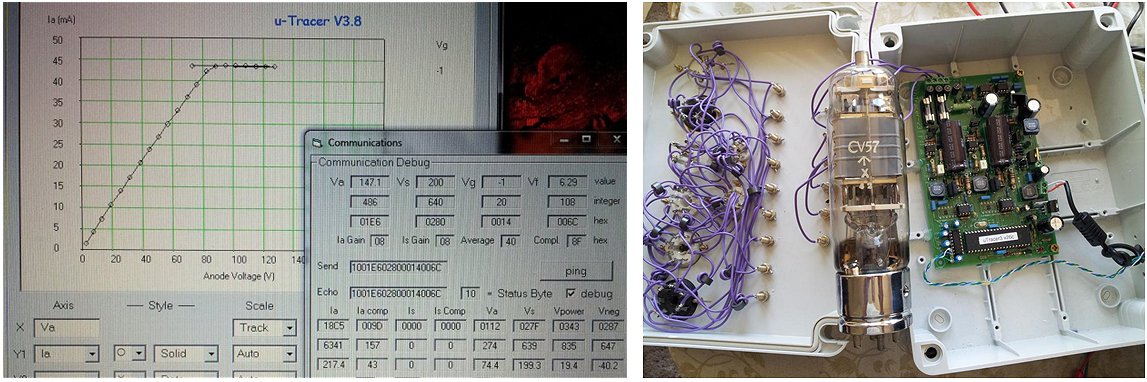
Figure 26.3 left, “the singular case of the folded curve”, right, The beast that “killed” Paul’s uTracer!
Looking at the graph we observe that the trance starts quite enthusiastically with a nice straight line as we should expect for a resistor. Then the current suddenly saturated at about 45 mA, and then the strangest thing of all, folds back so that the final part of the curve is drawn in reverse direction! What on earth is going on here?
The fact that the curve starts as a nice straight line up to currents of several tens of milliamps tells us that the high voltage switch is working reasonably well. If the switch was leaking more than a few milliamps, the boost converter wouldn’t be able to charge the reservoir caps. However, the current is completely wrong! At 80 V a 340 ohm resistor should result in a current of 80/340 = 236 mA, while only 40 mA is measured. This can mean two things: either there is something wrong with the current measurement circuit, or the high-voltage switch is leaking current so that the voltage of the reservoir capacitor severely
 dropped between the moment the boost converter was switched off and the current was actually measured. The latter explanation cannot be true, because we just a moment ago concluded that the high-voltage switch wasn’t leaking too much! Additionally, wat we do know, is that at about 240 mA the current limiting circuit kicks in which keeps the current constant. This is exactly what we see happening, note that at 80 V the current through 340 ohm is 80/340 = 235 mA, only the current reading along the y-axis is indicating a too low value. So what we can conclude now is: 1. The high voltage switch is still operating and not heavily leaking, 2. The current measuring circuit is damaged (most likely diode D14 is leaking), 3. The current limiting circuit (T16) probably survived the accident.
For the next few measurement points the current remains constant which should be the case if the current limiting circuit is properly functioning. Now we come to the part where the curve “folds-back”. What should be realized is that the voltage which is plotted for each measurement point is the voltage of the reservoir capacitor immediately after the measurement pulse. So if the set point voltage of the reservoir capacitor was e.g. 150 V and the value being plotted 100 V, this means that indeed the capacitor was charged to 150V at the beginning of the measurement (otherwise the GUI would have given an error message) but that at the end of the measurement the voltage was reduced to 100 V. So in other words, the high-voltage switch is conducting continuously. From the plot we see that this starts to happen at around 120 V, So likely the accident has damaged the transistor in such a way that the breakdown voltage has been significantly reduced. After some more test runs the MJE350 indeed failed completely resulting in a time-out error message. Replacing D14, T16, T17, and T18 of course solved the problem.
”What happened?”
We will probably never know for sure what happened exactly when Paul traced the CV57, but we can do some logical thinking and make an educated guess. At the time of the incident the general consensus - and at that time I tended to agree - was that the CV57 was drawing so much current that “the uTracer was taken by surprise,” as Paul put it. Although this explanation may be perhaps emotionally satifying, it really doesn’t make sense.
First of all if we look at some of the traces Paul posted on the forum which were taken before the dreadful incident occurred, we find many examples (scroll down to second posting) where he drove a tube well into the 200 mA compliance limit - even for voltages up to 300 V - without causing damage to the uTracer. So what is so special about this tube that it caused so much damage already especially at much lower voltages?
The second issue I have is that, since the grid cut-off voltage is -800 V, the tube supposedly would draw enormous currents at very low anode voltages, but is that really the case? Unfortunately the only datasheet that I could find doesn’t give any curves, but it does give some test specifications:
If I interpret the test condition correctly, then the sum of the anode and screen current for the CV57 connected as triode should be around 75 mA at an anode voltage of 200V and a grid bias between -30 and -45V. But Paul clearly mentioned that the current already went into 200 mA compliance at very low voltages, far below 200V!
A possible explanation occurred to me when I was preparing this write-up and was preparing Figure 26.3. It was obvious that Paul never could have used any of the test sockets on his uTracer. So my guess was that he simply used some (rather long) test leads with, undoubtedly considerable inductance. An accusation he immediately pleaded guilty to. That did however create quite favorable (or unfavorable depending on your point of view) conditions for oscillations! To suppress oscillations, AVO developed a special way to connect tube sockets in a ring configuration in case long lead wires are inevitable. I also recommend this way of connecting the tube sockets in the construction manual. Some people have tried to do without, end did experience oscillations (James, half way down the page). So it could well have been that the CV57 was violently oscillating, thereby upsetting the overcurrent protection mechanisms. For me this is the most satisfactory explanation so far.
Anyway, for less than a euro worth on components the uTracer was up and running again. That’s the advantage of modern solid-state electronics, if you break a valve, something irreplaceable is gone forever. If you destroy a few transistors, you just replace them for a few cents. Nevertheless I would like to conclude with a statement from Paul: “Can I just say what a pain in the butt it is to remove transistors from a through board two sides soldered pcb when you have installed them tight.”
| to top of page | back to homepage | to part I |
Many people have asked my for a possibility to use the uTracer to quickly test a tube for its most important parameters like Rp, gm and mu, without the need to go through the time-consuming plotting of a complete set of curves. Starting from version 3p10 this functionality has been implemented as an option in the GUI. In this section we will review how the Quick Test option can be used, how it works, and just for my own documentation how the software is organized.
Most quick reference tube manuals don’t give complete sets of curves for tubes, but only cite the most important parameters in an optimal bias point. If we take the EL84 as an example, then the optimal bias point is given as Va=250 V, Vs=250 V, and Vg = -7.3V, and the most important parameters in that point are Ia=48 mA, Is=5.5 mA, gm=11.3 mA/V, Rp=38 kohm. We have to distinguish between directly measurable parameters and derivatives. Two parameters which can be measured directly at the given bias point are the anode and the screen currents. Other parameters like the plate resistance, the transconductance (mutual inductance) and the amplification (mu) cannot be measured directly, but are derivatives from the tube’s characteristics. The transconductance for example is the first derivative of the anode current to the control grid voltage (∂Ia/∂Vg) at the specified bias point, and the plate resistance is the inverse of first derivative of the anode current to the anode voltage (∂Va/∂Ia) at the bias point.
For a triode where we only have the anode current which is simply a function of the grid- and the anode voltages: Ia(Vg,Va) there are only two derivatives: the transconductance (gm) and the plate resistance (Rs). The amplification factor mu can simply be calculated from mu=gm*Rp. For a tetrode/pentode the situation is already much more complex. Here we have to deal with the anode current (Ia) as well as the screen current (Is) which in principle are functions of all three terminal voltages so: Ia(Vg, Va, Vs) and Is(Vg, Va, Vs). Now there are no less than 6 derivatives which all have a physical meaning and which may be relevant for the design of a circuit:
Figure 27.1 Possible derivatives for a pentode
Some of these derivatives are more naturally presented as a resistance such as the plate and screen resistances, while the others are better presented as transconductances. In the “standard” GUI the derivatives are obtained by first measuring the complete curve, fitting a polynomial to the curve, analytically differentiating the curve and finally plotting the derivative. Although this method produces nice smooth curves as a function of bias, it is in most cases sufficient to know the derivatives in a particular bias point. In this case the derivative can be approximated by drawing a straight-line through two points Vo-δV and Vo+δV, where Vo is the bias point and δV is a small offset. The smaller δV is chosen, the more accurate the approximation will be, but also the more sensitive the result will be for noise in the measured data. In principle now only 6 measurements are required to calculate all the derivatives for a pentode shown in Figure 27.1, a seventh measurement gives the currents in the bias points itself. For a triode only 5 measurements in total are needed.
Figure 27.2 Quick Test of an excellent EL84 (6BQ5)
The “Quick Test” option which measures all the derivatives in a specified bias point has been implemented as an alternative for a full curve characterization.
The use of the Quick Test option is pretty straightforward:
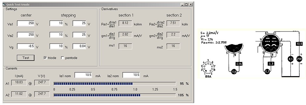
Figure 27.3 Quick Test of an ECC82 (12AU7) double triode. The plate resistance (Rp), transconductance (gm) and voltage amplification (mu)
are simultaneously measured for both sections.
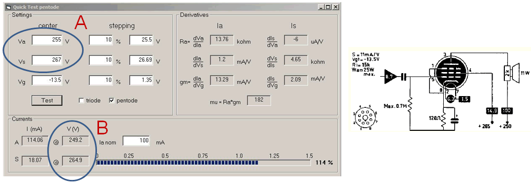
Figure 27.4 Quick Test of an excellent EL34 (6CA7). To obtain the desired bias voltages: Va=250 V, Vs=265 V (circle B) it may be necessary to increase the set point values slightly (circle A).
Inside the GUI
The code that goes with the triode and pentode Quick Test forms is limited to the processing and updating of the variable fields. After a variable is entered the routine “ProcessFields” is called to check if the value that was entered is within the allowed range, but also to check if the resultant measurement points are within the capabilities of the uTracer. Suppose e.g. that a nominal anode voltage of 280V is entered combined with a δV of 40V. Then this would result in two measurement points, one at 240V and one at 320V, which is higher than the maximum 300V supply range. In this case δV is re-calculated as 300V – 280V = 20V.
The communication between the triode and pentode Quick Test forms and the main program is done though a number of public variables which hold the nominal bias values and the δV values in percentages. When needed in either the main program or in the Quick Test forms the actual δV voltages are calculated from the nominal values and the stepping values in percentages.
The actual measurements are implemented in the main form in a very straightforward manner using much of the infrastructure already present for the tracing of curves. The routines “DoQTTMeasurement”, “ComposeQTTMatrix”, and “AnalyzeQTTMatrix” take care of the triode quick test, while routines “DoQTPMeasurment”, “ComposeQTPMatrix”, and “AnalyzeQTPMatrix” take care of the pentode quick test. The DoMeasurement routines are almost identical to the standard “DoMeasurement” routine except that they call different routines to compose and analyze the measurement matrix. The composition of the measurement matrices is done point by point based on the nominal bias voltages entered and the stepping values. The correct value for the heater voltage is obtained through a trick: by calling the standard “ComposeMatrix” routine we know for sure that the correct value of the heater voltage is in the appropriate column of the measurement matrix. Since there are only a few points in the measurement matrix the measurement itself only takes a few seconds. After the measurement the derivatives are calculated in routine “analyze matrix” routines.

10th October 2013, 25 years at Philips Research celebrated with friends.
| to top of page | back to homepage | to part I |
Although I have my own ideas about new features and improvements for the GUI, I was also curious to find out the wishes of the ever growing legion (now approaching 250!) of uTracer owners. So end last year I used one of these very nice and free internet services to make my own poll with the question “Which feature would you like to be added to the uTracer (GUI).” To my surprise over 140 people responded, and many took the effort to add their own whish, next to the five pre-defined multiple choice options. The result after 3 months is shown in Fig. 28.1. Clearly favorite is the possibility to test semiconductors, although I have to say straight from the beginning, that that will be limited to n-type MOSFETs and npn BJTs only. It is also my favorite, and high on my list of things to do when outdoor temperatures make soldering and tinkering on the uTracer4 less appealing.
Some of the wishes like higher voltages / currents and continuous sweep from negative to positive grid biases are simply impossible with the current uTracer3 hardware, but will be taken into account for the uTracer4 (if that one will ever see the light). Other ideas which can be realized in software will certainly be considered (I am particularly intrigued by the idea of making the screen voltage a function of the anode voltage). The second favorite improvement, was a means to improve the grid voltage calibration. Already from a few people I got questions about the accuracy of the grid bias at very low voltages. I myself am only a very casual user of the uTracer, and really only interested in the global functioning of a tube and the shape and particularities of their characteristics. However, it appears that for certain tubes (especially those with a high transconductance) and circuits, a tenth of a volt grid bias can make quite a lot of difference. As will be explained later there is unfortunately a limit to the accuracy that can be achieved. Having said that, it is also true that with an improved calibration procedure a significant improvement is possible. In this section the new calibration procedure will be explained. It has been implemented in “beta release” 3.11.2 and is available for testing.
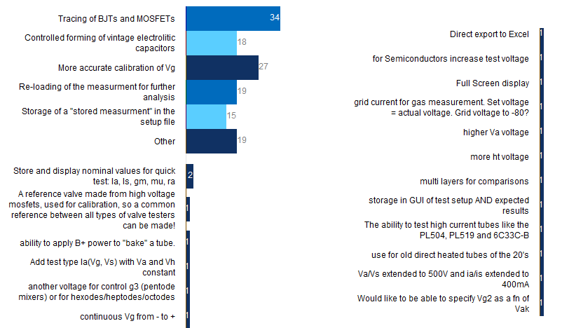
Figure 28.1 Results from the 2013 web-poll.
How the new calibration procedure works
The first observation is that, because of the way the grid bias is generated, there is a limit to the accuracy that can be achieved. It will be remembered that the grid bias is obtained by low-pass filtering and amplifying a Pulse Width Modulated (PWM) signal generated by one of the one-board PWM generators of the PIC in such a way that a duty-cycle of 0% corresponds to a grid bias of 0V, while a duty-cycle of 100% corresponds to -50V. The PWM generator has a resolution of 10 bits which means that the duty-cycle can have 1024 values. Consequently the smallest step in the grid bias is 50/1024 ≈ 50mV. At first sight that doesn’t sound too bad. Certainly for higher grid bias values this results in a pretty good resolution, however, as the grid-bias decreases the relative resolution dramatically decreases. For a grid-bias of -0.2 V e.g. a step of 50 mV amounts to 25% relative resolution! So with the uTracer hardware we can never do better than that.
This doesn’t mean that there is no room for improvement. The way the grid bias is calibrated at the moment is based on an approximation whereby the transfer function between the set-point grid bias is related to the PWM duty-cycle by a single straight line. Figure 28.2A shows how it is done. The relation between the duty-cycle (n) and the set-point grid-bias (Vset) is given by a n = Vset ⋅ C ⋅ λ40, with C = 1023/50. During the calibration, the actual grid bias is measured, and the user adjust the value of λ40 in such a way that a set-point of -40V exactly corresponds to a measured value of -40V. Although this gives a pretty good result for grid-biases down to several volts, it was found that for very low grid bias values the error could by quite significant, especially when tubes with a high transconductance and/or low pinch-off voltage are traced.
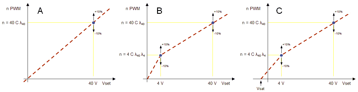
Figure 28.2 (A) Current grid bias calibration, and improved calibration based on two (B) and three (C) points.
A first step to improve the calibration procedure was to introduce a second calibration point at a much lower voltage. Since the first calibration is done at -40 V, I chose the second calibration point at a tenth of that value at -4 V. The transfer function between the set-point value and the PWM duty-cycle is now approximated by two straight lines as shown in Fig. 28.2B. The relation between the set-point and the PWM duty-cycle in the second calibration point is given by n = 4.0 ⋅ C ⋅ λ40 ⋅ λ4. After the user has calibrated the grid-bias at -40V, the grid bias is next calibrated at -4V by adjusting λ4. For λ4 one of the three spare calibration values on the Calibration form is used. Note that the default value for the calibration values is 1.0. So if the default value of 1.0 is used the value in duty-cycle in the second calibration point reduces to n = 4.0 ⋅ C ⋅ λ40 which coincides with the original calibration curve (Fig. 28.2A). In this way the new software remain compatible with the old calibration file meaning that if the user for one reason or the other does not feel the need to perform the extended calibration procedure, the old calibration file can be used resulting in the old grid bias values.
Unfortunately that is not the end of the story. As explained in one of the previous sections the output voltage of the grid-bias circuit can never exactly become zero. The saturation voltage of T6 and T7 limit the minimum grid voltage to approximately -50 mV. The saturation of T6 becomes noticeable for very low grid-bias values, and needs to be compensated for. This is done by introducing a third calibration value (Fig. 28.2C). By giving Vsat a value in the order of -80 mV, it is possible to somewhat compensate for the saturation of T7, although an output voltage of exactly zero volt can never be reached. Vsat is set by using one of the remaining two spare calibration parameters on the calibration form in such a way that the range of 0.9 – 1 - 1.1 of the calibration parameter corresponds to a Vsat range of -0.2 - 0.0 - 0.2 Volt so that the default calibration parameter value of 1.0 again corresponds to the old situation ensuring backward compatibility of the calibration file.
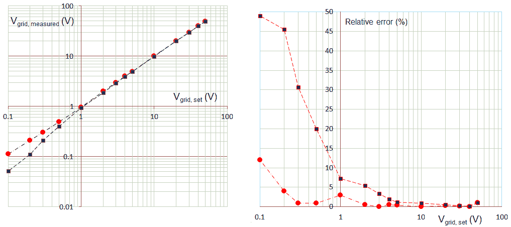
Figure 28.3 The accuracy of the new calibration procedure (red) compared to the old procedure (black).
In Fig. 28.3 the accuracy of the grid-bias voltage using the old single point calibration procedure is compared to the new procedure. Figure 28.3A shows - on a log-log scale - the measured grid-bias versus the set-point values. Figure 28.3B compares the relative accuracy of the two methods versus the set-point values. Down to -0.1 V the accuracy is within the theoretical limit of 50 mV.
The calibration procedure step-by-step.
The new grid-bias calibration procedure will be integrated in the next GUI release version 3.11. Until that release is available it can be evaluated in “beta release” 3.11.2 (and higher) available Here. For the calibration connect a DVM between the grid and cathode terminals of the uTracer, and use the measurement set-up as shown in the figure below. Note that the anode and screen voltages have been set to 25V to avoid dangerously high-voltages on the work-bench, and to minimize the time needed to discharge the high-voltage reservoir capacitors.
Recommended calibration procedure:
|
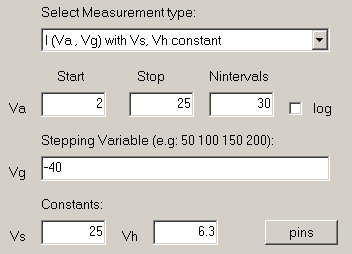
|
| to top of page | back to homepage | to part I |
Every radio tube exhibits a certain degree of non-linearity. As a result the output signal is distorted as compared to the input signal. Mathematically this means that when a pure sine wave signal with a certain frequency ω (=2πf) is applied to the grid, the anode not only carries a sine wave with the amplified fundamental frequency ω, but also sine waves with frequency components 2ω, 3ω, 4ω etc. These are called harmonics, and the whole process is called harmonic distortion. The amount of distortion is an important figure of merit for amplifiers, and it is therefore of interest to know how much, and what type of distortion a certain tube introduces.
Really the best way to obtain that information that is to build and test the amplifier! The second best thing is to perform a (number of) DC measurements on the tube, and to extract an accurate equivalent circuit model e.g. using the ExtractModel models and software. The behavior of the circuit can now be simulated using a circuit simulator such as LTSPICE. When all the non-idealities of all components such as parasitic capacitances and inductances are included in the simulation, this method provides an accurate prediction of the circuit behavior, including its non-idealities.
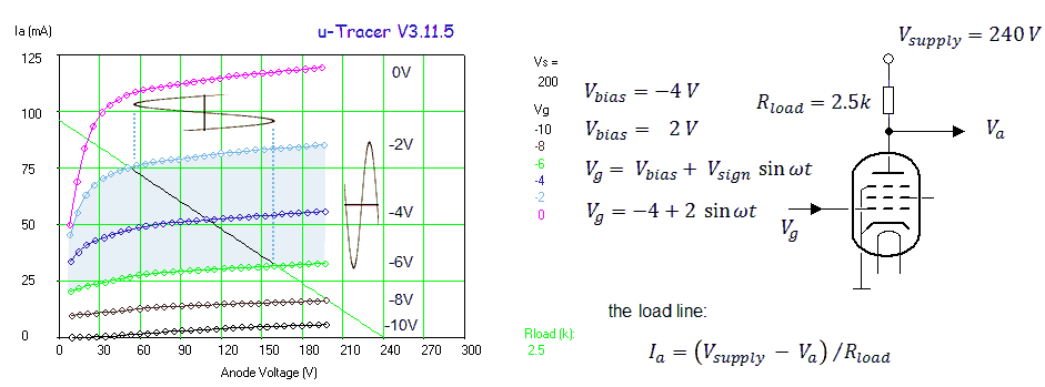
Figure 29.1 Graphical evaluation of the anode voltage as a function of the grid voltage.
Although the circuit simulation route is very accurate, most designers will start with a straightforward visual analysis of the output characteristics of a tube. A study of this set of curves will give experienced designers an idea of the gain and linearity, and the optimal load impedance, power supply voltage and bias point. The first step is to assume that the anode of the tube is connected to the high-voltage power supply by means of a simple resistor. This resistor “translates” the current sinked by the tube into a voltage, and fixes the relation between the anode current and anode voltage to a straight line which can be drawn in the set of curves. Note that the slope of this line is completely determined by the value of the load resistor and the supply voltage. The transfer characteristic of the tube from grid voltage to anode voltage can now be constructed by intersecting the set of curves with the load line. In the example of Fig. 29.1 a grid bias voltage of -4 V was used onto which an AC signal with an amplitude of 2 V was superimposed. From the intersection with the lines corresponding to grid voltages of -4+2 = -2 V and -4-2 = -6 V the swing of the anode voltage is found. At first inspection the average anode voltage is about 105 V, and the amplitude of the AC signal is about 55 V, corresponding to a gain of ca. 25. The selection of the optimal load line and the bias point obviously depends on many factors, and a full discussion is beyond the scope of this manual. A nice design example can be found here.
Apart from the gain, also the distortion can be estimated from the output characteristics and the load line. In the areas where the distance between equal steps in the grid voltage corresponds to equal steps in the anode current, the distortion is expected to be low. In the pre-computer area people have come up with all kind of ingenious schemes to determine the distortion directly from the output characteristics by means of graphical analysis. An extensive explanation of how that can be done is given by Reich in Theory and Applications of Radio Tubes (1944). It requires an evaluation of the anode current in a large number of strategically chosen bias points along the load line followed by some straightforward algebra. Not really complicated, but cumbersome and prone to mistakes. What is even worse, the method requires a large number of curves for different grid voltages, or a visual interpolation between curves. All-in-all not really a practical method to get a quick impression of the distortion.
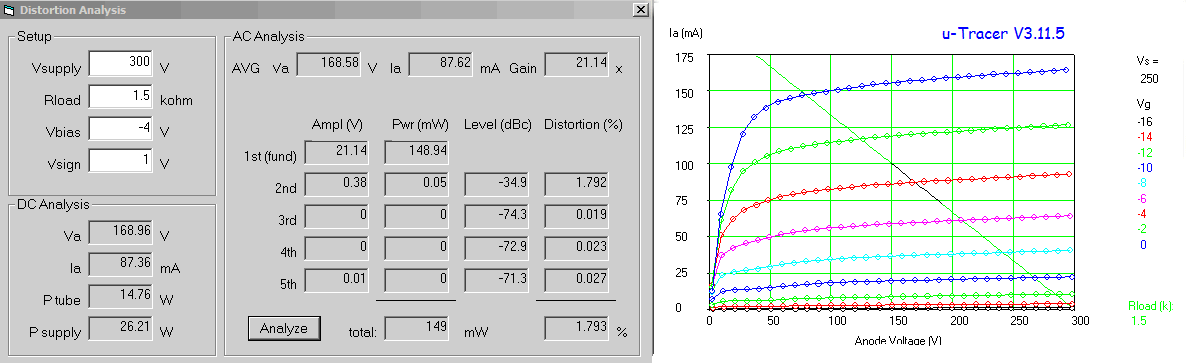
Figure 29.2 Example of the “distortion analysis form” and a corresponding set of curves.
The distortion analysis tool in the uTracer GUI pretty much follows the same route, but uses the advantages of the massive computing power available in modern computers. First the program takes the measured output curves and calculates a 2D qubic spline matrix. With this matrix it is possible to accurately interpolate the anode current Ia for any combination of anode voltage (Va) and grid voltage (Vg), provided that they fall within the minimum and maximum values of Va and Vg used for the measurement. Next a linear solver determines the intersection points between the load line and the output curves for a large number of points using the qubic 2D spline to interpolate between the actually measured points. Again a spline is used to provide a smooth transfer curve from grid voltage to anode voltage. This transfer curve is used to calculate the anode voltage resulting from a pure sine wave grid voltage. Finally a Fast Fourier Transform (FFT) is used to determine the harmonics in the output signal. It sounds complicated, but it is really pretty straightforward and only takes a fraction of a second.
The distortion analysis can only be performed when a valid set of output curves is displayed in the graph on the main form. The set of curves can be a measurement performed in the same session, or a set of curves reloaded from a setup file. The distortion analysis form is opened by pressing the “Distortion” button in the measurement analysis section on the main form. The distortion analysis form consists of three sections: “Setup,” “DC Analysis,” and “AC Analysis.” In the setup section the supply voltage (Vsupply) and the load resistor (Rload) for the load line can be specified, as well as the DC grid bias (Vbias) and the amplitude of the sine wave grid excitation (Vsign). Note that the amplitude is defined as shown in Fig. 29.1 Pressing the “Analysis” button plots the load line into the graph, and performs the DC and AC analysis. Note that on the load line the swing of the grid voltage is highlighted. The DC values of the anode current and voltage are directly obtained from the intersect point between the load line and the output curve corresponding to the grid bias voltage (Vbias). The power dissipated in the tube (Ptube) and the power supplied by the power supply (Vsupply) are calculated from the DC anode current and voltage and the power supply voltage.
Figure 29.3 Formulas behind the distortion analysis form.
The section “AC analysis” shows the results of the FFT calculation. From Fourier analysis theory it is known that any periodic signal with frequency ω can be written as an (infinite) sum of sine wave functions with frequencies ω, 2ω, 3ω, …, with amplitudes A0, A1, A2, A3 …. The first term A0 represents the average anode voltage. For very small signal amplitudes the average anode voltage equals the DC anode voltage. However, when the signal amplitude increases, part of the AC anode signal will be rectified due to non-linearities of the tube. The rectified voltage will add to the DC voltage causing a shift in the average anode voltage. The second term in the Fouriers expansion is the fundamental frequency component. It is basically the “wanted” component in the output signal. The amplitude of this component divided by the amplitude of the AC grid signal determines the gain (A1/Vgrid).
The other terms represent the second, third and higher harmonics. On the form the second up to the 5th harmonic have been included. Of every harmonic, (including the fundamental) the power it generates in the load is listed. Furthermore, for every harmonic its distance below the carrier (in dBc) is given. Finally, the distortion factor, which is the ratio of the amplitude of the harmonic with respect to the fundamental component, is calculated.
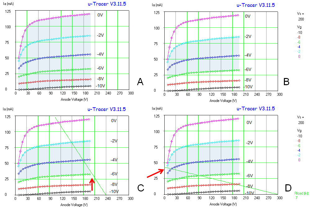
Figure 29.4 The measurement area and the load line.
Limitations
Although the distortion analysis tool can accurately interpolate between measurement points within the measurement dataset, it cannot extrapolate outside of it! Fig. 29.4A shows an example of a measured set of output curves. For the point of illustration, the anode voltage was swept starting from 10 V; normally the lowest anode voltage of 2 V would always be used. In this example, the grid voltage was stepped from -10 V to 0 V. The colored area gives the range of the measured data set. All intersections of the load line with the curves for the selected grid bias and grid signal amplitude have to fall within this colored area! For the proper use of the distortion analysis tool a number of guidelines and limitations have to be taken into account. When these limitations are violated a warning message is issued. In this section these limitations will be discussed in relation to the warning messages issued:
>>> The x-axis variable must be Va or Vs!
A fairly obvious requirement. The distortion analysis form can only be evoked when an output-characteristic type of measurement has been selected.
>>> At least 3 curves with each 5 points required!
To make the spline algorithm work, a minimum set of curves and a minimum set of points per curve is necessary. Here, a bit arbitrary, the minimum number of curves has been set to three, with a minimum of five points per curve.
This raises the question what number of curves and number of points per curve is optimal. Obviously more curves and more points per curve will result in a higher accuracy, but also increase the measurement time. In the EL84 examples in this section, the grid voltage was incremented with steps of 2 V. In a test the interpolated values at the 1 V intervals were calculated and compared to measured values. The error in all cases was less than 1%. In general the Ia(Va,Vg) characteristics of tubes are rather smooth and well behaved. A limited number of curves and points is therefore in most cases sufficient to “capture” the tube, and the example shown in this section gives a good idea of an optimal set of curves and points.
As already mentioned, it is possible to store the measurement together with the measurement set up. In this way it is possible to analyze a set of curves that was obtained in a previous measurement session.
>>> Signal amplitude below minimum measured Vg! & Signal amplitude above maximum measured Vg!
This simply means that the maximum input signal (Vbias + Vsign) has to be equal or less than than the maximum grid voltage used in the measurement, and that the minimum input signal (Vbias – Vsign) has to be equal or higher than the minimum grid voltage used in the measurement.
>>> Vgrid outside measurement plane, right-side. Decrease Vsupl or Vsign; or increase Rload!
This situation is best explained by an example. Assume that for the set of curves of Fig 29.4B a grid bias (Vbias) is applied of -4 V, and that the amplitude of the input signal (Vsign) is 2 V. The input voltage will now swing between the grid bias lines marked with -6 V and -2 V (colored area). The left side demarcation of this area is given by the minimum anode voltage that was specified in the measurement, while the right side border is determined by the maximum anode voltage used. For certain combinations of Vsign, Rload and Vsupply it is possible that the load line does not intersect with the all the curves in the colored area. This situation is shown in Fig 29.4C. Note that for low input voltages the load line does not intersect the curves for the lowest grid voltages. In this situation a warning message is given and no further calculations are made, and the user has to decrease the supply voltage or the signal amplitude, or to increase the load resistance.
>>> Vgrid outside measurement plane, left-side. Increase Vsupl; or decrease Vsign or Rload!
A similar condition can occur on the left side of the graph. Figure 29.4D shows the situation where the load line fails to intersect the highest grid bias curves. The remedy here is to increase the supply voltage or to decrease the input amplitude or load resistance.
>>> Maximum number of iterations exceeded, please save problem and report.
Please save the problem and report the problem!

Cadzand
| to top of page | back to homepage | to part I |
If there is one thing which is on top of the wish list of most uTracer owners, it must be higher anode and screen voltages. Higher voltages was one of the motivations to start the work on the uTracer 4. Now that the work on the uTracer 4 has come to a (temporary?) hold – more about that later – it is a good moment to see if it is possible to squeeze out a few more volts from the uTracer 3. A first step towards higher voltages will be to increase the speed of the high voltage switch.
A short recap concerning the high voltage switch
So why is the maximum voltage in the uTracer 3 limited to 300 V in the first place considering that the reservoir capacitors are rated for 400 V? The reason is that I wanted the uTracer to be short circuit proof over the entire voltage range. Let’s recapitulate what happens during an overcurrent or short circuit event: the first thing that will happen is that the hardware current limiting circuit will kick in, limiting the current to about 225 mA. It does this by allowing for some voltage drop over the high-voltage power transistor. The moment the maximum current limit is exceeded, the processor is interrupted causing the processor to switch off the output. In uTracer vocabulary the whole event is called “a compliance error.” In case of a short circuit, the high voltage transistor has to accommodate the full voltage of the reservoir capacitor at maximum current! To give an example: at 300 V and 225 mA this means an instantaneous dissipation of 70 W! Fortunately, this only lasts a very short time, so that the temperature rise of the output transistor is very small.
Reality is sometimes more complicated. The current distribution over the surface of the silicon chip inside (any) transistor is usually not completely homogeneous. As a result - especially in bipolar transistors - hot-spots can form: the warmer regions attract more current, these regions become even warmer thereby attracting even more current, becoming even warmer etc. As a result the transistor can burn down in a tiny spot. MOSFET transistor transistors are much more stable in this respect, but have other drawbacks such as higher capacitances, and the lack of availability of high-voltage low on-resistance pMOS devices.
To prevent damage to the high voltage switch, the total short circuit event should be kept as short as possible. During the development of the uTracer 3 it was found that the main bottleneck in reducing the pulse time during a short circuit was the time needed to switch the high voltage switch off. Whereas the microcontroller responds in only a few microseconds, it takes about 15-20 µs for the high voltage switch to follow. With such a “long” on-time, it was found that the maximum output voltage had to be limited to 300 V to withstand repeated short circuits. The first goal therefore is to reduce the switching speed of the HV switch, especially the off switching time. The aim is to make this a retrofit so that it can be used in combination with the existing uTracer 3 hardware
The Improved HV switch
Rather then first discussing all the ins and outs of the improved high voltage switch circuit (left), Fig. 30.1 directly shows the final circuit diagram.
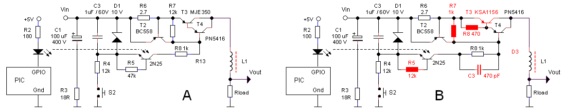
Figure 30.1. The improved high-voltage switch (right) compared to the old circuit. The components that have been modified are indicated in red. Note that apart from these modifications also the integrating capacitors at the Op-Amps have to be removed!
The switching speed delay of the circuit consists of four components:
To my surprise one of the largest contributions to the total delay turned out to be the delay introduced by the inverting Op-Amp, and then more specifically not the delay of the Op-Amp itself, but the delay as a result of the integrating capacitor. During the development of the original HV-switch circuit this capacitor was not implemented. It was added at a later stage to reduce the noise level in the current measurement. However, I didn’t realize the quite significant delay it also introduces in the switching behavior of the high-voltage switch. Fortunately it appears that this capacitor can be skipped without increasing the noise level noticeably. Probably the final PCB version is is much less sensitive to noise than the experimental perf-board version.
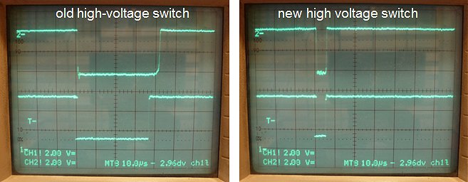
Figure 30.2. The response to a complete short-circuit condition of the old hv-switch circuit (left) compared to the new hv-switch circuit. The transistor on-time reduces from 40 us to 6 us! The lower trace shows the hv-switch command signal from the processor (low = switch on). The upper trace shows the voltage across the 18 ohm current sense resistor. The output voltage was set to 200V.
Apart from the elimination of the integrating capacitor, the MJE350 transistor was replaced by a KSA1156. Although the MJE350 has a breakdown voltage in excess of 400 V, it is only specified to 300 V. The KSA1156 is specified for a BVceo of 400 V, but in fact has a breakdown voltage in excess of 500 V. The few other modifications concern measures to increase the speed of the transistors by removing the excess charge from the base of the transistors by means of optimized emitter-base “bleeder resistors.” In Fig. 30.2 the response time of the new circuit (6 µs) is compared to the response time of the old circuit (ca. 40 µs) in the case of a complete short circuit condition. The circuit is able to withstand repeated short circuit pulses at the maximum voltage of 400 V.
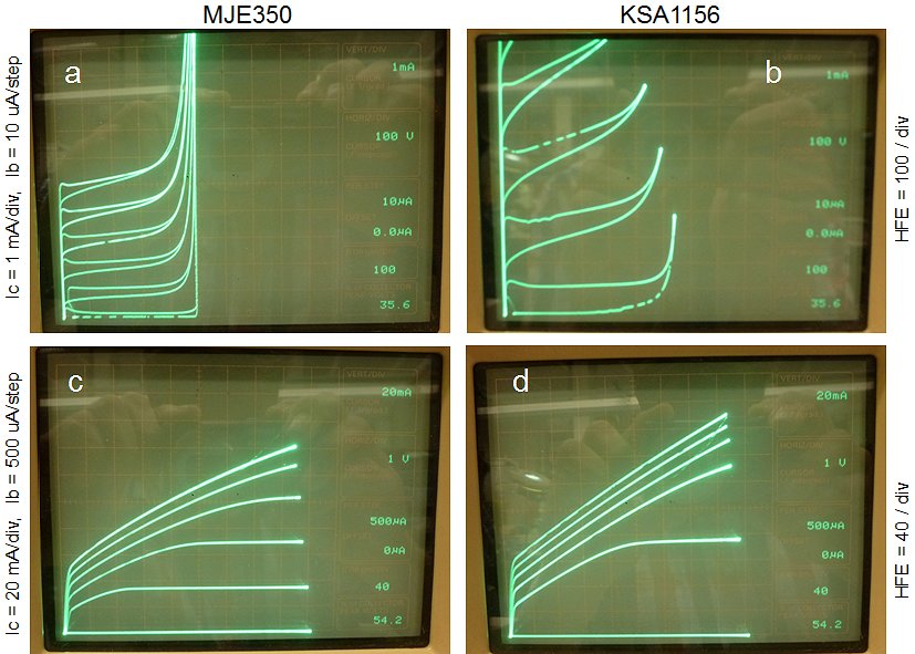
Figure 30.3. a&c Output characteristics of an MJE350 at low currents (a) and at high injection conditions (b). Figures b&d give the same measurments for a KSA1156.
The test circuit
One of the things that made the development of the original hv-switch circuit a bit difficult was that the entire switch is at high potential level, which in this case can be as high as 400 V. To make probing of the circuit easier, a test circuit was made whereby the entire hv-switch section was shifted to ground level.
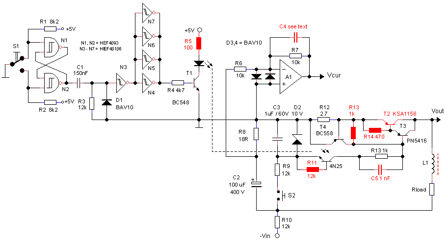
Figure 30.4. Test circuit used in the development of the new HV switch. The PIC is replaced by a one-shot pulse generator and the whole HV switch has been shifted to ground level to facilitate easy probing with the oscilloscope.
Figure 30.4 shows the new test circuit. The pulse is generated by the same circuit as was used in the development of the original test circuit. The fact that the HV-switch circuit is essentially floating with respect to ground and driven by an opto-coupler made it very easy to shift it to ground level. In this case the reservoir capacitor is charged with a negative voltage with respect to ground. Note that whereas in the normal circuit the voltage drop over the current sense resistor is negative with respect to ground, it is positive in this circuit.
Circuit Details
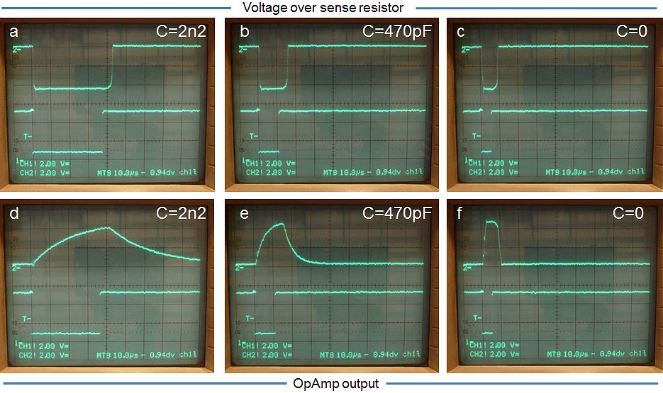
Figure 30.5. This set of measurements shows the drastic effect of the integrating capacitor across the Op-Amps. In all measurements a 560 ohm resistor was connected to the output and a 200 V pulse was used so that the hardware current limit was activated. The lower trace in all photo’s shows the hv-switch command signal from the processor (low = switch on). The upper trace in the top row of pictures shows the voltage across the 18 ohm current sense resistor, while the upper trace in the bottom row of pictures shows the output voltage of the Op-Amp. The three columns from left to right show the result for C=2n2 (standard), C=470pF and no integrating cap. For the HV-switch the improved circuit was used.
The high voltage switch is controlled by the processor which in return gets its input information about the current level from the voltage drop over the 18 ohm current sense resistor. Since this voltage drop is negative with respect to ground, it is inverted with an inverting Op-Amp.
During the development of the original uTracer circuit (on perf-board) quite a high noise level was observed in the measured current that could be drastically reduced by decreasing the bandwidth of the Op-Amp by means of an integrating capacitor. What was not fully realized at that time was that that would also increase the delay in the current compliance loop. Figure 30.5 shows the HV-switch control signal (lower trace) and the output of the inverting Op-Amp for a capacitor value of 2n2, 470pF and when no capacitor is used. It appears that by simply removing the capacitor the response time can be increased by almost a factor of 4! Fortunately this is possible without increasing the noise level significantly, probably due to the fact that the PCB version of the circuit is much less sensitive to noise than the experimental perf-board version.
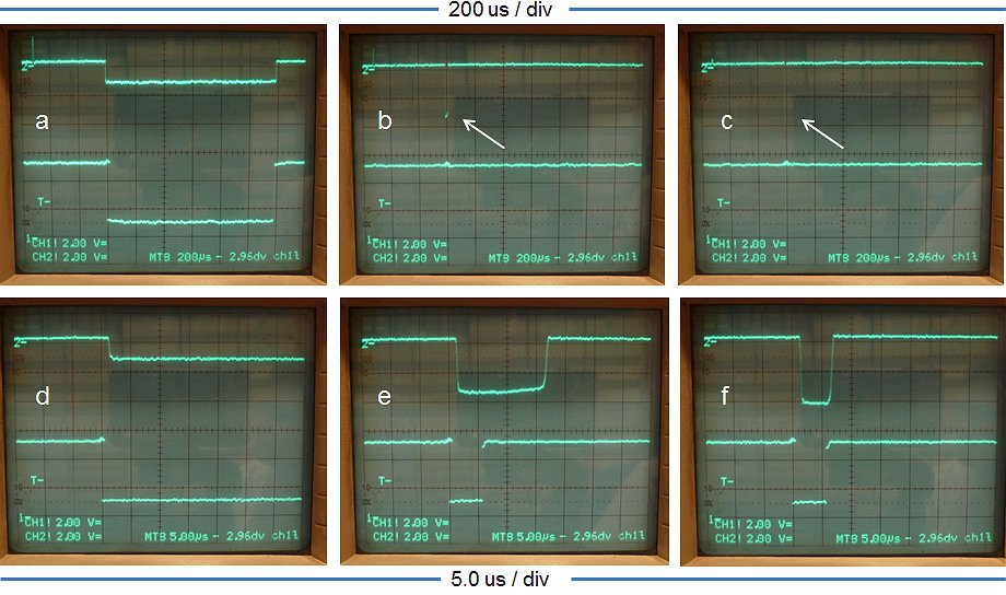
Figure 30.6. This set of measurements shows the difference between the software and the hardware compliance limits (see also text). In these measurements the output of the uTracer is connected to a 560 ohm resistor and the improved high-voltage switch circuit is used. The software compliance limit is set to 200 mA. The lower trace in each photo shows the hv-switch command signal from the processor (low = switch on). The upper trace shows the voltage across the 18 ohm current sense resistor. The measurements in the upper and lower three photo’s are identical but taken with a different time-base setting. In photo’s a&d the output voltage was 50V (no compliance), in photo’s b&e the output voltage was 120 V (software compliance), and in photo’s c&f the output voltage was 200V (hardware current limiting + software compliance).
It is important to realize that in the on-state the HV-switch can operate in three modes:
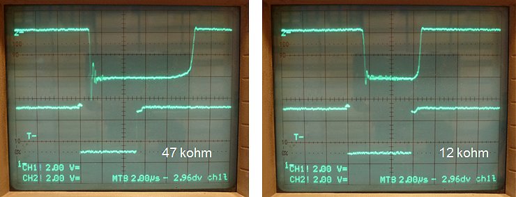
Figure 30.7. This measurement shows the effect of decreasing the value of the emitter-base “bleeder” resistor of the photo-transistor in the opto-coupler from 47 kohm (original value) to 12 kohm. The lower trace shows the hv-switch command signal from the processor (low = switch on). The upper trace shows the voltage across the 18 ohm current sense resistor. For this measurement the improved HV-switch circuit was used. A 560 ohm resistor was connected to the output and a 200 V pulse was used so that the hardware current limit was activated.
A further important delay is associated with the turn-off time of the transistor in the opto-coupler. Transistor opto-couplers are notoriously slow elements. This is related to the fact that in order to make the photo-transistor light sensitive it needs to have a large base that can store a lot of charge. A well known trick to decrease the turn-off time of a bipolar transistor is to add an external emitter-base “bleeder resistor” which helps discharging the base. Already in the old hv-switch
An 47 kohm emitter-base bleeder resistor was used to decrease the turn-off time of the opto-coupler. In the improved circuit the bleeder resistor was further decreased to 12 kohm, again decreasing the turn-off time of the opto-coupler (Fig. 30.7). Although this greatly increases the speed of the opto-coupler, the resistor is now draining away so much photo-current during the on-time that it has become difficult to turn the photo-transistor fully on. By decreasing the series resistor of the LED of the opto-coupler from 180 to 100 ohm this could be remedied.
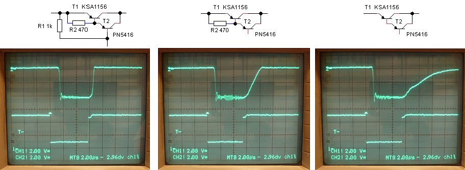
Figure 30.8. This set of measurements shows the effect of the emitter-base “bleeder” resistors in the hv-switch Darlington pair. Without bleeder resistors the current decays almost logarithmically corresponding to the decay of the injected electrons in the base of the transistor. The lower trace shows the hv-switch command signal from the processor (low = switch on). The upper trace shows the voltage across the 18 ohm current sense resistor. For this measurement the improved HV-switch circuit was used. A 560 ohm resistor was connected to the output, and a 200 V pulse was used so that the hardware current limit was activated.
A more or less similar story holds for the high voltage transistors in the output Darlington. Also here the turn-off behavior can be improved the using an optimized emitter-base bleeder resistor. Figure 30.8 shows the difference in turn-off behavior when one or two of the bleeder resistors are omitted. Without bleeder resistors a more or less logarithmic decay of the collector current of the Darlington is observed.
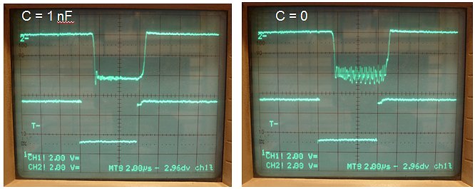
Figure 30.9. During a full short-circuit condition the hardware current limiting circuit tends to oscillate (right). A small capacitor across the basse resistor of the Darlington pair tames this oscillation. The lower trace shows the hv-switch command signal from the processor (low = switch on). The upper trace shows the voltage across the 18 ohm current sense resistor. The output voltage was set to 200V.
When a full short circuit condition (Rout = zero) occurs, the short circuit current has the tendency to oscillate (Fig. 30.9 right), during the very short time that the output transistor is on. The oscillations are very likely the result of the high gain in the hardware current limiting circuit consisting of T4 and R6. The oscillations increase in frequency with increasing output voltage (all under full short circuit condition), most likely because at higher voltages the depletion capacitances are smaller. One or two ferrite beads proved to be very effective in suppressing the oscillations, while a simple 1 nF capacitor at the base of the Darlington almost eliminated them (Fig. 30.9 left). Since these measures are more effective at higher frequencies, at low output voltages (0-50 V) some oscillations persisted but since the amount of energy in the circuit is relatively small in that case (scales with V squared), they are considered to be harmless.
In conclusion we can say that the switching behavior of the high voltage switch can be greatly improved with a few simple measures. The next steps will be to actually increase the output voltage of the boost converter and to build up a full version for rigorous testing.
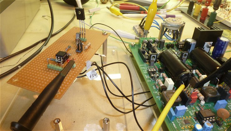
Figure 30.10. My “test uTracer” in combination with an external HV switch on perf-board was used to test and debug the new circuit. After a lot of software development the past few months it is great to do some experimental work again! (October 2014)
GUI modifications
Most people probably never realized that getting higher voltages out of the uTracer is just a matter of exchanging two resistors, one for the anode and one for the screen supply! The only thing the GUI transmits to the uTracer hardware is a number (0-1024), and the hardware adjusts the voltage of the reservoir capacitors in such a way that the ADC value matches this number.
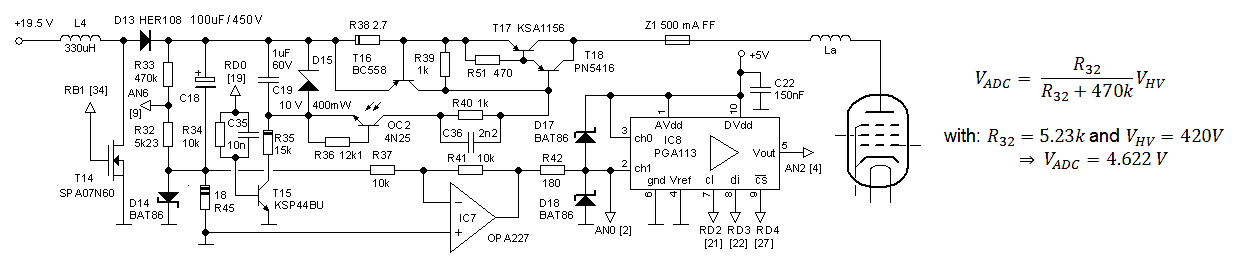
Figure 30.11 uTracer3+ boostconverter circuit
As an example assume that the supply voltage is 20V and that we request an anode voltage of 300V. This means that the high voltage capacitors need to be charged to 300+20 = 320 V. In the standard uTracer3 configuration 320 V over the reservoir capacitor corresponds to (6.8/(6.8+470))*320 = 4.57. The corresponding number which is send by the GUI to the hardware is (4.57/5.00)*1023 = 934. Note that by simple lowering the value of R32 a higher output voltage will be generated for the same number. For the uTracer3+ the value is R32 was lowered to 5k23 so that a voltage of 420 V corresponds to an ADC input voltage of 4.622 V which in turn corresponds to the binary value (4.622/5)*1023 = 946. The penalty that is paid in this way is that the resolution by which the output voltage can be set is slightly reduced from 320/934 = 0.343 V/step to 420/946 = 0.444 V/step, a small price to pay.
Obviously to make the voltages that are entered by the user and the voltages that are being displayed in the output data correspond to the actual voltages, also the conversion factor (basically the resistance value of R32, Fig. 30.11) has to be modified in the GUI. To avoid having to maintain two separate versions of the GUI a provision was created so that a single GUI could be used for both version 3 as well as version 3+. In the Calibration form, a new frame is created with two selection buttons where the user can select the appropriate version (Fig. 31.1). By clicking the “Save to Calibration File” button, the selection is subsequently stored in the calibration file so that it is automatically reloaded the next time the GUI is started. To enable this, the format of the calibration file had to be extended. Normally the last number stored in the file would have been the COM port number. In the extended format the COM port number is stored as a negative value to indicate that it is an extended file and that more data is following. The next number is than the version number: 1 = uTracer3, and 2 = uTracer3+. The file is ended with -1 to indicate the end of the file.
Despite the fact that the Calibration forms contains an explicit warning to correctly set the version, there fortunately is room for an error! When in case of uTracer3 hardware the GUI is accidentally set to version3+ the maximum capacitor voltage will never be more than (6.8/5.23)*320 = 416 V. When in case of uTracer3+ hardware the uTracer3 GUI is selected to maximum voltage will never be more than (5.23/6.8)*420 = 323 V. In both cases the hardware will survive. Note that although the incorrect voltages are generated, the measurements will nevertheless incorrectly indicate the voltages programmed. Don’t let yourself be fooled, and set the correct version number!
| to top of page | back to homepage | to part I |
In this section the step-by-step conversion of a 300 V uTracer3 into a 400 V uTracer3+ will be described. This conversion consists of two parts: the installation of the new GUI, and some hardware modifications. For the hardware modifications a small kit containing all the necessary components is available from my “How to Order” page.
Installation of the new GUI.
For the 400 V uTracer3+ hardware the latest version of the GUI (version 3.11) needs to be installed. The installation of the new GUI is very simple! Since you already will have an older version of the GUI running, all the necessary auxiliary OCX components and dll files have already been installed and registered. Installation of the latest GUI is now only a matter of installing a new executable:
Figure 31.1 The uTracer version can be selected and stored in the new calibration form in the GUI.
Hardware modifications.
Figure 31.2 shows the complete circuit diagram of the uTracer3+ hardware. The components which have been changed are high-lighted in red.
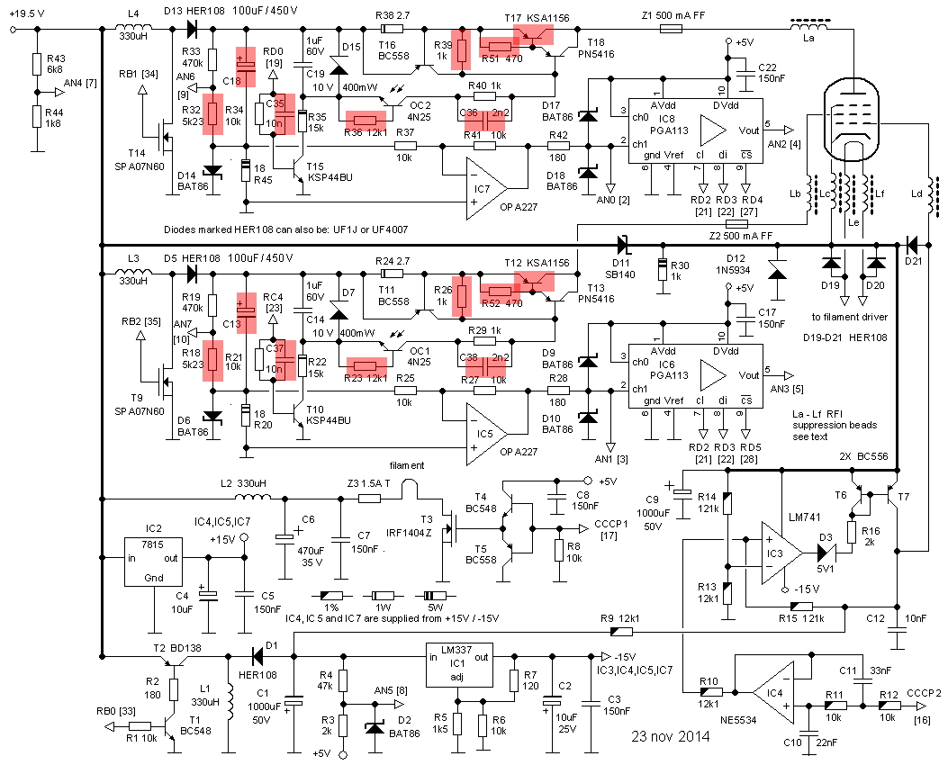
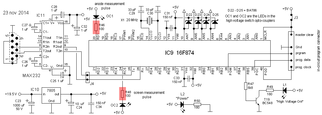
Figure 31.2 Complete circuit diagram of the 400 V uTracer3+
In the following a step-by-step modification of the hardware will be described. Changing components on a heavily populated PCB is never a pleasant task which is why I have tried to figure out a procedure which makes life a easy as possible. From the circuit diagram it can be seen that some resistor values have been changed with respect to the uTracer3+. In all cases the new resistances will be lower. Rather than removing the old resistor, in most cases I have chosen to lower the resistance by placing a second resistor in parallel to the original resistor on the bottom side of the PCB. This eliminates the need for a messy removal of the original resistor. In some cases completely new components had to be added, and the placement of these components on the bottom side of the PCB could not be avoided. However, there will undoubtedly be people who prefer to simply exchange the resistors where possible. That is why in the conversion kit I intend to supply also the resistors for direct replacement have been included.
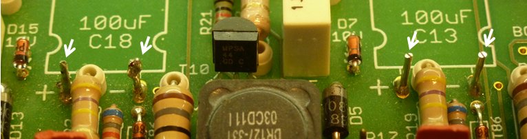
Old 100 uF / 400 V removed.
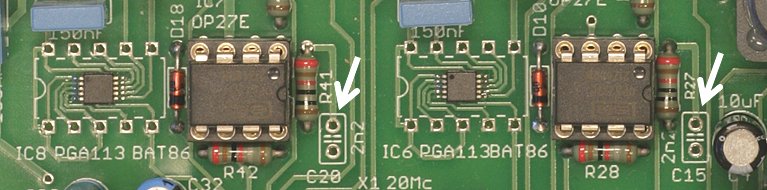
C15 and C20 removed.
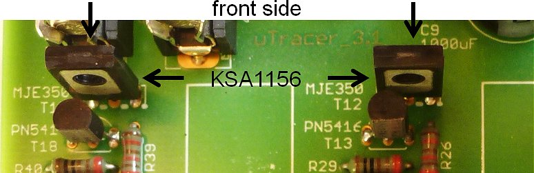
T12 and T17 replaced by KSA1156 transistors.
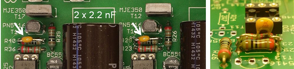
C36 and C38, two 2.2 nF capacitors are soldered directly over R29 and R40. Note that the photograph on the right was taken at an earlier stage during the construction when not all the components on the board were placed yet.
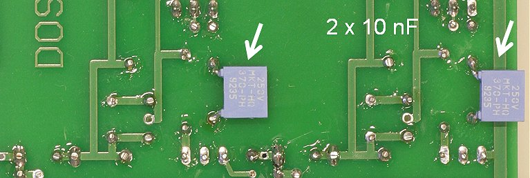
C35 and C37 are soldered over R21 and R34 on the backside of the PCB.
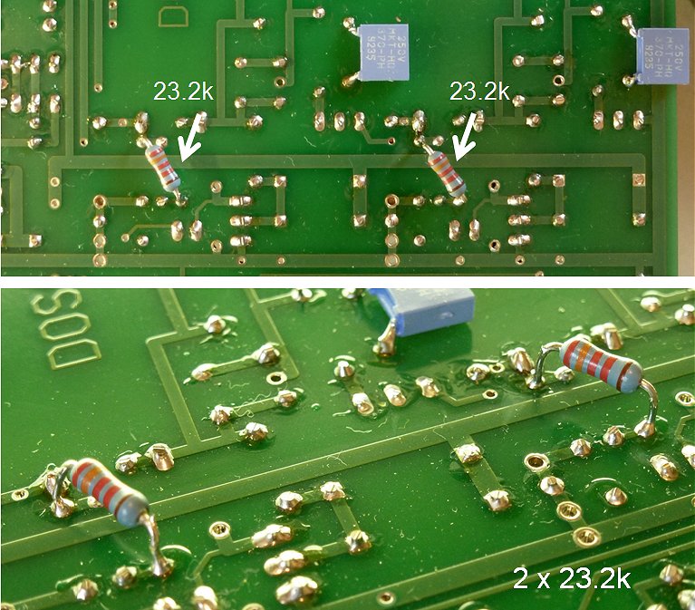
Modification of R18 and R32 by placing two 23k2 resistors in parallel to the original 6k8 resistors (top view and side view).
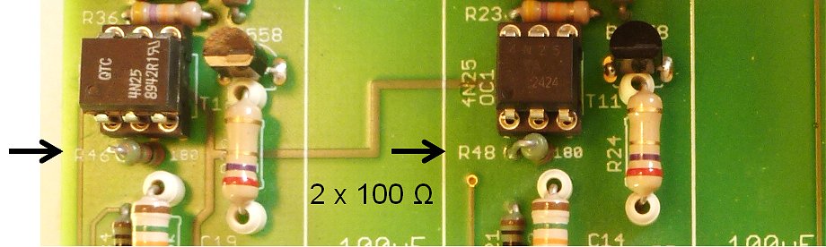
Replace R46 and R48 by 100 ohm resistors
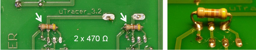
R51 and R52 are 470 ohm resistors over the outer pins of the two KSA1156 transistors.
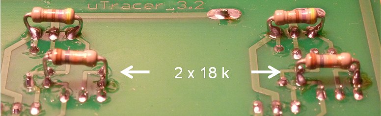
Modification of R23 and R36 by placing two 18k resistors in parallel to the original 47k resistors.
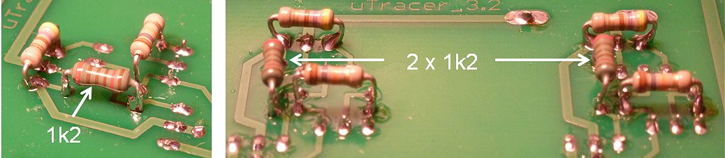
Modification of R26 and R39 by placing two 1k2 resistors in parallel to the original 12k resistors.
Replacing the high voltage reservoir caps for 450 v types completes the conversion.
Calibration
A small calibration of the output voltages is necessary:
Component list
The table below gives lists the components needed for the conversion of the utracer3 into the uTracer3+. The working voltage of the capacitors is not relevant and the resistors are 1/4 or 1/8 Watt type.
I am offering a small conversion kit which includes all the components listed below:
| 2x | 100 uF / 450 V | e.g.: Mouser 647-UPZ2W101MHD |
| 2x | KSA1156 | e.g.: Mouser 512-KSA1156YS |
| 2x | 2n2 | e.g.: Mouser 594-K222K15X7RF5TK2 |
| 2x | 10 nF | e.g.: Mouser 871-B32529C103J |
| 2x | 23k2 | for complete replacement 5k23 |
| 2x | 1k2 | for complete replacement 1k0 |
| 2x | 18k | for complete replacement 12k1 |
| 2x | 470 ohm | |
| 2x | 100 ohm |
| to top of page | back to homepage | to part I |
Several users of the uTracer have pointed me to a small but annoying problem related to the grid bias supply. From anomalies in the curves at low grid biases (close to zero) they concluded that the grid bias during the actual measurement must be lower (more negative) than the DC value to which it was calibrated! The difference is especially notable in tubes with a very low cut-off voltage like the ECC83 (12AX7). Measurements indeed revealed that during the 1 ms measurement pulse, the grid voltage gradually becomes more negative with a total deviation in the order of a 100 mV from the calibrated value!
The grid bias supply
Lets for a moment recollect how the grid bias supply works. The grid bias supply is controlled by
one of the PWM outputs of the PIC micro controlled. The output produces a 19 kHz square wave output
with a variable duty-cycle. This PWM signal is fed into the low pass filter constructed around IC4 (Fig.32.2).
When the duty-cycle is 0% the output voltage of the low-pass filter is 0 V. When the duty-cycle is 100%, the
output voltage is Vdd = 5V. OpAmp IC3 amplifies the output voltage of IC4 by a factor of -10x and references it
to the cathode terminal. So when the output voltage of the IC4 is 0 V the grid bias with respect to the cathode
is 0 V, and when the output voltage of IC4 is 5 V the grid bias with respect to the cathode is -50 V. Due
to a practical limitation, the grid bias can never become exactly zero volts, but saturates at -50 mV.
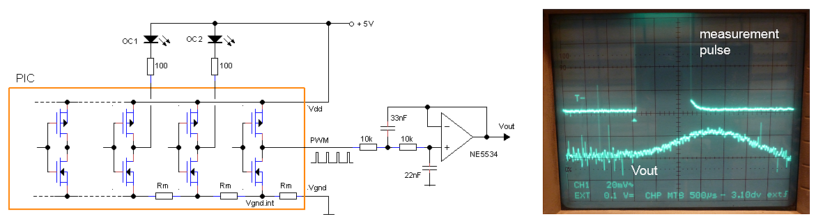
Figure 32.1 Explanation of the origin of the problem (left), the measured increase in voltage at the output of the low-pass filter during a measurement pulse (right).
The cause of the problem
An investigation into the circuit with the scope quickly revealed that the problem could already be seen at the output of the low-pass filter (IC4). Figure 32.1 shows an oscilloscope trace taken at the output of the low-pass filter. It shows a gradual increase of output voltage of up to almost 10 mV during the measurement pulse. Of course, after amplification by a factor of -10x this results in a drop in grid bias of 100 mV. The most likely causes for the problem could be a variation of the ground potential or a variation in the supply voltages. Measurement of the ground reference and the two supply lines showed however that these were very stable. The only remaining cause therefore could be a variation in the PWM input signal coming from the PIC!? To be absolutely sure that the problem originated from the PIC, the low-pass filter circuit was reproduced on a piece of perf-board and supplied by an independent power brick (fig. 32.3). The result was exactly the same!
After some puzzling and thinking the problem was traced back to the opto-couplers! When the opto-couplers
were removed from their sockets, the grid voltage remained absolutely stable. Given the fact that the supply
voltages of the PIC are stable I came to the following explanation of the problem. During the measurement
pulse the IO’s of the PIC sink quite a high current. Apparently the resistance of the internal interconnects
inside of the PIC, in combination with these high currents result in a voltage drop of ca. 10 mV (Fig. 3.1).
The problem became worse going from the uTracer 3 to the uTracer 3+ since the current through the opto-coupler
LEDs was roughly doubled in this version!
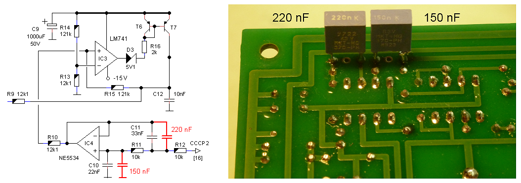
Figure 32.2 Addition of two capacitors (red in the schematic) to fix the problem and a suggestion how they can be added to the backside of the PCB.
A solution
Having found the cause of the problem, an (elegant) solution had to be found. Several solutions were considered. A good solution would be to insert a buffer stage in between the PWM output of the PIC and the low-pass filter. Even better would be to include LED drivers for the LEDs in the opto-couplers. Both solutions are however rather drastic in the sense that they require a rather messy intervention with the electronics on the board. A non-hardware solution would be to add an additional offset variable to the calibration form. However, this would significantly increase the complexity of the calibration procedure for the grid supply, and would require the use of an external grid bias during the calibration procedure in order to be able to compare the internal grid bias during a pulse with an exactly known reference bias.
The solution I opted for in the end makes use of the property of the low pass filter that the output voltage of
the filter lags behind to variations in the input signal. The lower the corner frequency of the filter, the larger the
delay. Remember that right up to the start of the measurement pulse the PWM output of the PIC is okay, and that only
during the 1 ms that the LEDs are on the internal ground level of the PWM output is lifted up 10 mV. So if we lower
the corner frequency enough, the delay between input and output can be increased so much that the measurement pulse
is over before the output can change significantly! Fortunately the time between the moment the grid bias value is set and
the moment the actual measurement pulse takes place is long enough (ca. 30 ms) to allow for this solution.
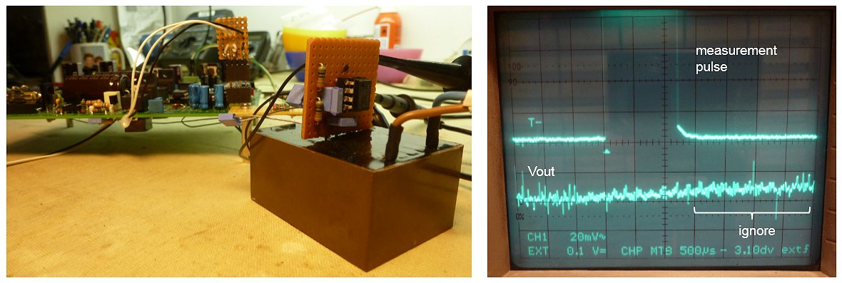
Figure 32.3 Test setup (left) and a trace of the output signal of the low-pass filter after placement of the two additional filter capacitors
By simply placing two capacitors parallel to the two capacitors in the low-pass filter, the corner frequency of the
filter is lowered to 60 Hz, while the settling time is increased to approximately 10 ms. Figure 32.2 shows the placement
of these additional capacitors in red in the circuit diagram, and also shows how the capacitors can be added to the
backside of the PCB. It shouldn’t take more than 5 min to make the modification! The oscilloscope trace in Fig. 32.3
shows how the placement of two additional capacitors almost completely removes “the bump” in the grid bias during the
measurement pulse.
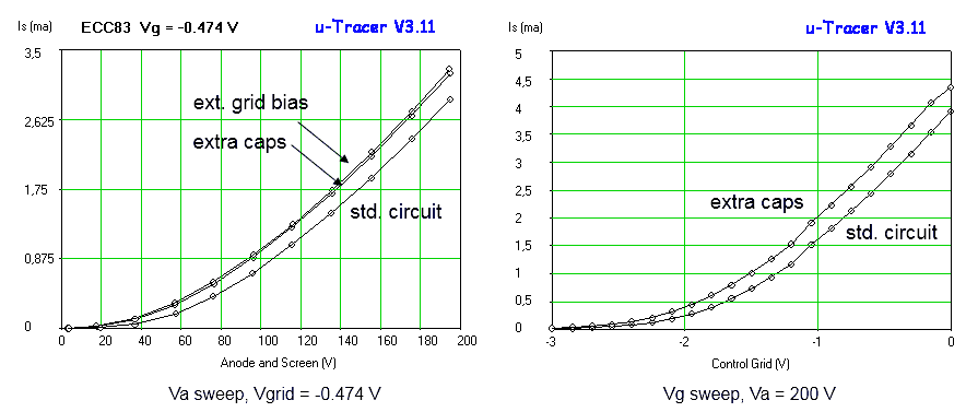
Figure 32.4 Effect of the circuit modification on two traces taken from an ECC83 (see text below).
The left graph in Fig. 32.4 shows an anode voltage sweep taken from one section of an ECC83 for three different grid bias configurations. I first set the GUI to a grid voltage of -0.5 V and measured the grid voltage during the sweep of the unmodified circuit, while at the same time the anode the current was plotted. The grid bias turned out to be exactly -0.474 V (I used an uncalibrated uTracer for this experiment). Then, using a resistive voltage divider and a variable power supply, I made an external bias supply of exactly -0.474 V and applied it to the tube and again recorded the anode current. As can be seen from the graphs there is a significant difference between the two currents indeed indicating that the actual grid bias during the measurement pulse is lower (more negative) that the “DC” value measured. Next the two extra capacitors were added and again the anode current was measured with the same grid bias setting. The new curve now almost overlaps with the external bias curve indicating that the solution indeed works. For reference Fig. 32.4 also shows a grid bias sweep for the same tube with and without the additional capacitors.
Feel free to experiment by increasing the capacitors even further. The time between the moment when the grid bias is programmed and the measurement pulse is long enough to allow the capacitors to be increased by at least a factor two or three. Try to maintain a capacitance ratio between C11 : C10 of 1.5 : 1
Martin Manning made a small investigation of the effect of the modification described above. He directly replaced C11 and C10 by a 330 nF and 220 nF capacitor respectively, Read his findings here.
Finally, another interesting method to increase the accuracy would be to limit the grid bias range to say 0 to -5 V. In principle this can be done by changing the values of R10 and R13 from 12k1 to 121k. For the graphs it would just mean that you have to measure from 0 to -50 V to get a range of 0 to -5 V. The quicktest would however not function correctly since the derivatives would be calculated the wrong way. However, some people found that the grid bias circuit started oscillating by reducing the gain of the circuit, so I would not recommend this mod.
| to top of page | back to homepage | to part I |
| to top of page | back to homepage | to part I |
Yours truly in front of the PASCAL, one of the first computers made by Philips Research in 1960. It was used at Philips Research for calculations on hot air engines, television and semiconductors and was in use until 1972. It consisted of 1200 vacuum tubes, 10000 transistors and 15000 diodes and dissipated 10 kW. PASCAL stands for “Philips Akelig Snelle CALculator” (Philips awfully fast calculator). It is now in the faculty museum of the faculty of “Electrical enigeering, Mathematics and Informatics” of the Technical University in Delft. (Photo: Adnan Noor)
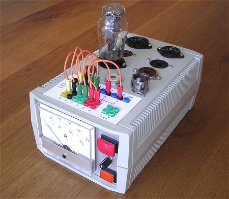