The term "mixed-signal" is usually reserved for circuits and ICs that process both analog and digital signals. In that sense the title "A mixed-signal LED clock" is perhaps misleading since this is a digital clock from beginning to end. However, the readout is analog and since the beast had to be given a name, I a called it my "mixed-signal" clock.
Somewhere in the middle of the eighties, when I was studying, I joined the ECA: the Eindhoven Computer Association, a microcomputer club in Eindhoven. Although I am not a member anymore, they still exist and have now been active for more than 25 years [1]. Being situated in Eindhoven, the club obviously had close links with Philips, and regularly obtained surplus supplies of components of various kinds. I remember that these components could be bought for fl 0.10 (10 guider cents) a piece on every Tuesday evening. At one time they had a batch of LEDs in various shapes and colors. In those days a LED was not quite the common component it is today. The availability of these LEDs in these beautiful colors and nice shapes suggested the idea for a clock with an analog clock face.
Normally, I never bother about making a printed circuit board for my circuits.
I prefer working on these cheap prefabricated pertinax breadboard cards.
However, for the circular face of my LED clock I had no other alternative
than to etch a PCB (Fig. 1).
I made it in the summer of 1987, and after I had placed
the LEDs and finished the wiring, I put it into a drawer. There it was forgotten
due to more pressing projects (girls and examinations).
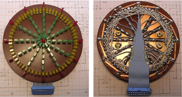
Figure 1. Front and backside of the face of the LED clock.
Two years ago I found it again and decided to finish the clock. It actually
became my first PIC processor project. The circuit of the clock contains
no real surprises. A (literally) striking feature about this clock is that
it has a real mechanical bell which strikes the hours. It gives the clock
quite an homely appearance, and it has became a much valued member of our
household.
As mentioned, the circuit of the "Mixed-Signal" clock is rather straight
forward.
Since the second, minute and hour LEDs could be time multiplexed,
the LEDs are connected in a matrix (Fig. 2).
The anodes of the LEDs are connected to the rows, the cathodes to the columns.
For the hours hand, five LEDs connected in series have been used. This
additionally sets the supply voltage to a minimum of 12V.

Figure 2. Organisation of the LED matrix.
Both for the anodes as well as for the cathodes, drivers with
discrete transistors have been used. The two resistors of 330 ohm
in the anode drivers set the current through the LEDs and hence their brightness.
The left 330 ohm resistor (connected to rows A...E) sets the current
through the seconds and minutes LEDs while the right LED (connected to row F)
sets the current through the hours LEDs. You will have to determine the
proper value of these resistors experimentally. The value of 330 ohm is just
a starting value and depends on the exact supply voltage, and the color of the
LEDs used. Especially the resistor for the hours LEDs will be much smaller,
typically something in the range of tens of ohms.
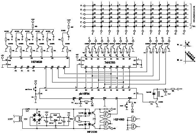
Figure 3. Circuit diagram overview of the mixed-signal LED clock. Clicking on the figure will open a window with a detailed circuit diagram in pdf format.
The 16F84 processor used here is a little bit out dated and no longer
in production. I used it because of the simple fact that I had it lying
around. The more modern 16F628 is pin compatible and will perform equally well. The 16F628 controller requires some minor software modifications. The source and hex files for both the 16F84 and the 16F628 have been included in the download section at the bottom of this page.
The 16F84 has too few I/Os to address all the anode and cathode drivers
directly (Fig. 3).
A 74HC563 8 bits latch was used to extend the number of outputs
by another 8 bits at the expense of a latch enable signal taken from port A.
The eight outputs from the latch, together with the lowest 4 bits of
port B from the PIC drive address the cathode drivers.
Since only one of the anode rows is switched on at any given moment,
a HEF4028 1-of-10 decoder could be used to activate one of the six rows using
only 3 bits (A0...A2). These bits are connected to the higher 4 bits of port B.
To prevent unwanted illumination of LEDs during the multiplexing of
data to the 74HC563, I/O bit A3 from port A is used to completely disable
all the anode drivers.
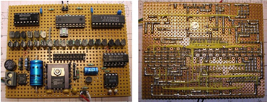
Figure 4. Front- and Backside of the processor and LED driver board.
As in most of my clocks, the frequency reference is derived from the mains frequency. On my NIXIE I clock page I discuss the "standard" circuit I developed for this. In this version the filter around the HEF4047 one-shot and the 50Hz to 1Hz divider have been implemented in software. The working however is exactly the same.
A distinct feature of this clock is the mechanical bell which strikes the
hours. For this bell I have used the bell salvaged from an old analog
telephone (Fig. 5), but any doorbell with the interrupter removed will do.
The characteristic ping is obtained by energizing the bell from a charged
capacitor rather than from the 12V power supply. The 15 kohm resistor charges
the 10 uF electrolytic capacitor in less than half a second. When the
transistor is switched on, the charge in the capacitor is dumped in the
bell coil.

Figure 5. The bell salvaged from an old telephone connected to the clock.
Since the clock time base is derived from the mains, there was no real need
to run the PIC processor on a crystal oscillator, instead a simple
RC oscillator was used. This does however require setting
of the appropriate bits in the STATUS register during programming of the
processor.
Figures 4-6 depict how the circuit was built on a piece of breadboard, and
how the face of the clock is connected to the PCB.
At the bottom of this page both the assembler source as well as the assembled Intel hex code can be downloaded. The program is as simple as the hardware. The time is kept in three registers: SEC, MIN, HRS. Every second the program updates these registers. The program uses four tables to translate the values in these registers to the proper settings of port B and the 74HC563 latch so that the corresponding LED will light. Table MIN_L contains the latch data for the seconds and minutes while table MIN-B contains the port B data. The corresponding tables for the hours are HRS_L and HRS_B.
The backbone of the program is the timer 0 interrupt service routine. Timer 0 is
programmed so that the service routine is called every millisecond.
The routine performs the
following tasks: saving of working registers, reloading of timer 0,
filtering of 50Hz mains frequency, dividing the 50Hz mains to a 1Hz
timebase, input key debouncing, the scanning of the
multiplexed clock face, and the ringing of the bell (if required).
The working of the filter and the divider is straightforward
and analogous to the hardware implementation.
The display scanner uses an auxiliary
counter DISPL. This counter can have the values 1,2,3.
When the values is 3, the routine
displays the seconds, when it is 2 the minutes, and when it is 1 the hours.
DISPL is updated by the interrupt routine itself at every call.
The data in the SEC, MIN and
SEC registers is translated to the appropriate port data as described above.
Communication between the main program and the interrupt service routine is
done via flags NEWKEY and NEWSEC. When, for example the
routine has detected that the key was pressed, the NEWKEY is set.
This is detected by the main program, and after processing of the input the main
program resets the flag.
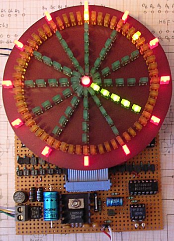
Figure 6. The clock during program development.
The main program consists of three parts. In the first part (label=INIT:) The variables, the interrupts and the timer are initialized. The second part (label=ADJ:) processes the adjustment of the clock. Here the same one buttom system is used that I also use in my other clocks: pressing the button once will start the hours to increment. By pushing the button again, the hours remain fixed while the minutes start incrementing. Pushing the button again will cause the incrementing to halt. A final push on the button at the full minute starts the clock. Since the clock does not ring the bell between 0:00 AM and 7:00 AM, it needs to know whether the time set is AM or PM. This is done in the following way: During the adjustment of the hours the 60 minute LED is lighted when AM, while the 30 minute LED is lighted during PM time. The last part of the program keeps the time stored in; SEC, MIN, SEC.
Since the values in SEC, MIN, and HRS are translated to the appropriate
output codes via took-up tables, the format used to store the data in
these registers is binary rather than BCD. Here a special trick is used.
The normal procedure to update the time would look as follows: increment SEC,
check if SEC has reached 3CH (3CH=60), if so clear SEC and increment MIN.
Although this is straight forward and easy to implement, I used an even
simpler method. Instead of incrementing the registers, the registers are
decremented! So 3CH corresponds to 00 (hand up), 3BH corresponds to 01,
3AH to 02 etc. The look-up tables translate this data to the appropriate
visible representation. The advantage is that now a single instruction
(DECFSZ) can be used to both advance the seconds and at the same time
check if a reset of the seconds and advance of the minutes is required.
The compressed file which can be downloaded here , contains the following files:
David Hathaway from the U.K. designed and made a PCB for the LED clock.
Click here to down load the artwork for this PCB.
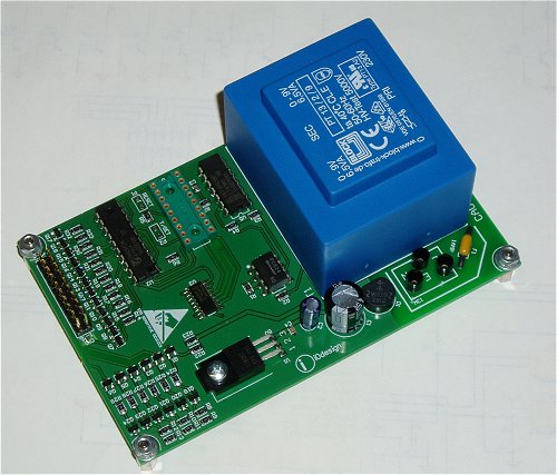
Figure 7. The PCB that David Hathaway made for the LED clock.

Figure 8. Another cool version of the clock made by David Setya Atmaja. He also made a very nice PCB and some alterations to both hardware and software (click here) to view his page.