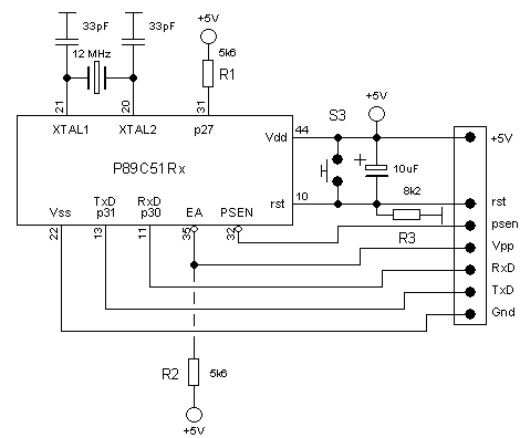
Figure 1 ISP interface at the processor side.
The P89C51RB2/RC2/RD2 family of microcontrollers are fully 80C51 compatible with many additional features [1]. The P89C51RB2/RC2/RD2 device contains a non-volatile 16kB/32kB/64kB memory. The flash memory is organized in blocks. The lower two blocks are both 8kB in size. The higher memory blocks are 16kB each. The flash memory can be programmed in three different ways:
Apart from the normal Flash memory, the processor also contains a piece of ROM code that is normally hidden from the user. This ROM code is the so called boots loader. By applying specific voltage conditions to some of the processors (I/O) pins during a reset pulse, this piece of ROM code is activated. As a result, after the reset, the processor will start to execute the boot loader instead of the user program (Flash program). The boot loader communicates to the user via a serial link using the on board UART. Via this modem link commands can be issued to erase blocks, program blocks by sending an Intel hex file, dumping memory blocks etc.
I used the P89C51RC2 processor for my first NIXIE clock.
The In System Programming possibility proved to be especially useful during the development of the program. I developed a simple interface to connect the processor
to my PC. On this page I will discuss this interface. After assembly of the assembler
code on the PC, the resulting hex file was loaded into the P89C51RC2. Under windows
there are several interface programs available like WINISP. I prefer to work under DOS,
so I developed my own simple communication program. This program allows you to
issue commands to the processor by simply pressing the function keys. The advantage
is that you can really follow what is going on on a byte level.
The on-chip boot loader is activated by: 1. forcing a reset by making RST high, 2. applying certain voltage conditions to some of the controller's (I/O) pins, and 3. remove the reset by making RST low again. The required voltage conditions are:
Figure 1 ISP interface at the processor side.
Figure 1 depicts the ISP interface on the processor side as I have used it in he NIXIE clock. Note that in Fig. 1
all other (I/O) pins not relevant to the ISP interface have been omitted.
The RC circuit around the RST pin is standard. I have included the RST signal in the
ISP interface, so that it is possible to issue a reset from the ISP board.
R2 makes EA high when the ISP interface is not connected so that in normal operation the internal Flash memory is executed. R2 additionally allows for EA to be pulled to 12V
by the ISP board.
Resistor R1 ties p2.7 to Vcc and at the same time limits
the current through p2.7 to a safe value when the pin is accidentally switched to an
output.

Figure 2 circuit diagram of ISP interface on the ISP board. The position of S1 as drawn in this diagram is for normal operation.
The processor is connected to the ISP board via a 7 wire flat cable.
Figure 2 depicts the circuit diagram of the ISP interface board itself.
A double pole changeover switch S1 is used to force the processor to the program
mode. S1a pulls PSEN low while S1b applies the 12V program voltage to EA/VPP.
The 12V program voltage is obtained from the 5V supply of the host by means
of a 5V to 12V DC-DC converter block. The DC-DC converter was salvaged from
an old PC Ethernet board. The advantage of a DC-DC converter is that the program
voltage is automatically removed when the processor is switched off.
Alternatively you can use an external 12V power supply, but then you have to make
sure that S1 is never switched to the program mode while the processor is switched off.
A MAX232 is used here in the standard configuration to translate the TTL levels to RS232
standards. If you processor application already has a RS232 interface connected
to the serial ports of the P89C51RC2, this interface can be used instead.
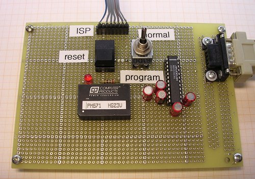
Figure 3 Close-up of the ISP interface board.
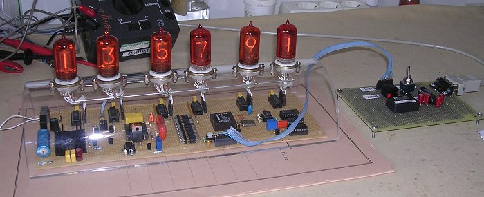
Figure 4 ISP board connected to the NIXIE clock during program development
Although I played around a while with the "official" ISP interface program WINISP,
I nevertheless decided to write my own interface program for two reasons. First I wanted
to understand what is going on on a bit and byte level. What better way to learn that by
doing it yourself? The second reason is more down to earth: the 486 Laptop I use in my
"shack" only runs DOS. As you might have understood by now, I am not a particular fan
of Windows! I really do not see the sense of filling my hard disk with hundreds of
megabytes of Windows shit, while all the programs that I have which run under DOS
are faster, simpler, more reliable and more transparent! So the interface program
was written in "good old" QuickBasic 4.5 (the compiler version)[4]. In the download zip
file I have included the source file of the program. If you have QB 4.5 running you can follow how it works.
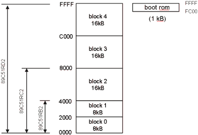
Figure 5 Flash memory configurations.
The Flash program memory of the P89C51Rx2 processors is organized into blocks as shown in Fig. 5. In erased state all memory locations contain FF. The memory is programmed byte by byte depending on the data in the Intel hex file transmitted to the P89C51Rx2. However, the memory can only be erased a block at a time. There are separate commands for the erasure of each individual block. Additionally the entire memory can be erased by a single command.
Okay, so how do these commands look like? Unfortunately they don't resemble plain English. Instead, the commands are an extension of the Intel hex file format. The Intel hex format was developed for the transfer of assembled machine code between the assembler and a memory/processor programmer. An Intel hex file is a readable ASCII file containing precisely defined records (lines). Each line starts with a semicolon (:) followed by the number of data bytes in the record, the starting address of the data, the record type, The actual data (usually up to 16 bytes) and a checksum. Excellent descriptions of the Intel hex file format can be found in [2,3]
In a "normal" Intel hex file usually only two record types are used. Record type 01
is used for the transfer of data, and record type 00 is used to indicate the end of the file. In the extended file format used here, additionally record types two to six have
been defined. The P89C51Rx2 datasheet contains a detailed description of these records
types. For example the record to erase block 4 is:
:0200000301C03A
Going from left to right 02 is the number of data bytes (01 and CO) 0000 is the address (don't cares in this particular command) 03 record type miscellaneous write functions 01 erase block instruction, C0 means block 4 and 3A is the checksum.
All this is quite a mouth full for such a simple command! For this reason I have programmed most of the commands "behind" functions keys, so that by simply pressing a single
key a complete record with instructions is send to the processor. Figure 6 shows the
window of the ISP program when it is run under DOS. The window consists of four parts.
The "sendfile:" line specifies the hex data file that you want to send to the processor
for programming. The next block on the screen is a summary of all the commands that are
available by pressing a function key. Note that ^F1 stands for control+function key, aF1 stands for alt+function key and sF1 stands for shift+function key. The "input from RomSim:" field shows the data send back by the processor (The program was originally
made to communicate with my EPROM simulator, and I forgot to change the name). The last field "output to RomSim:" shows the data as it is send to the processor.
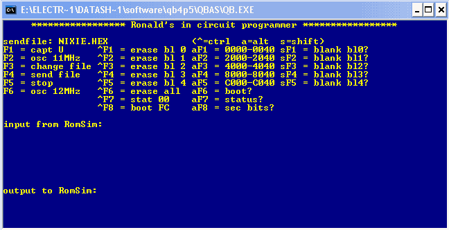
Figure 6 Program window of the ISP interface program.
In this section I will step by step go through a normal programming session. I assume that the ISP interface has been connected to the processor and the PC running the ISP interface program. The program is brought into the programming state by holding the reset button pressed while the toggle switch is changed from the normal to the program position. After releasing the reset button the processor should now be in the program mode.
The first thing that the processor has to establish is the baud rate used by the ISP program. This is accomplished by an automatic baud rate detection feature built in the processor's firmware. This feature requires that the first character to be send to the processor has to be an uppercase-U (function key F1). On receiving this "U" the processor calculates the baud rate used and responses by sending back a "." (A "." is in most cases the processor's response to a successful reception of a command record).
At this point communication with the processor is established. The processor now has to know the crystal frequency since this frequency effects the timing of the internal programming of the flash memory. I have preprogrammed two crystal frequencies: 11 MHz (F2) and 12 MHz (F6). By pressing either one of these function keys the correct record is send to the processor. 11 MHz is the rounded frequency in case a 11.059 MHz crystal is used. This crystal frequency allows for correct baud rate generation by the 80C51 UART, even at the highest baud rates .
Assuming that we want to load a program into memory block 0, we first need to erase this block. This is done by pressing ctrl-F1. Erasing a block takes a few seconds. After successful erasure of the block the processor responds with a ".". An additional blank check of block 0 can be performed by pressing alt-F1. Again a "." denotes a blank memory (all locations FF).
Now the hex file can be uploaded. To do this first the hex file needs to be specified. This is done by pressing F3 and entering the name of the hex file (the current path is the directory from which the ISP program is run). By pressing F4 the hex file is now send to the processor and programmed into the flash memory. Correct reception of the data is acknowledged with a "."
The first 40 bytes of a memory block can be checked by pressing shift-F1. This will cause the processor to display memory locations 0000H-0040H on the screen. The ISP program is terminated by pressing F6
In the preceding the software boot loader was activated by applying special voltage conditions to certain (I/O) pins during a hardware reset. It is also possible to activate the boot loader under software control. Additionally, it is possible to execute a custom boot loader after a reset.
To accomplish this the P89C51Rx2 processors contains two special Flash registers: the BOOT VECTOR and the STATUS BYTE. At the falling edge of reset, the P89C51Rx2 examines the Status Byte. If the STATUS BYTE is set to zero, power-up execution starts at 0000H, which is the normal starting address of the user's application code. When the STATUS BYTE is set to a value other than zero, the contents of the BOOT VECTOR is used as the high byte of the execution address and the low byte is set to zero. The factory default setting is 0FCH,
corresponding to the address FC00H for the factory masked ROM ISP boot loader. A custom boot loader can be written with the BOOT VECTOR set to the custom boot loader.
The compressed file which can be downloaded here , contains the following files: